Article

Fully DC Aggregation Topology with Power Self-Balancing Capacitors for Offshore Wind Power Transmission: Simulation Study

1
Electric Power Research Institute, China Southern Power Grid, Guangzhou 510663, China
2
State Key Laboratory of Alternate Electrical Power System with Renewable Energy Sources, North China Electric Power University, Beijing 102206, China
*
Author to whom correspondence should be addressed.
Electronics 2025, 14(17), 3422; https://doi.org/10.3390/electronics14173422 (registering DOI)
Submission received: 21 July 2025 / Revised: 20 August 2025 / Accepted: 25 August 2025 / Published: 27 August 2025

Abstract

This paper focuses on the Input-Independent Output-Series (IIOS) DC converters within fully DC aggregation systems, which enable independent submodule control and high voltage gain. DC aggregation systems experience output voltage imbalance among submodules due to offshore wind power fluctuations. The proposed isolated DC/DC converter topology incorporates power-balancing capacitors, leveraging intrinsic characteristics to achieve self-power balancing within the system. In addition, this paper proposes an innovative PFMT-PSMN hybrid control strategy that is well-suited for the proposed topology. Firstly, this study performs a time-domain analysis of the intrinsically power-balanced DC series-connected aggregation topology and elucidates the corresponding power-balancing principle. Secondly, based on soft-switching boundary conditions, a hybrid control strategy, PFMT-PSMN, adjusts phase-shift duty cycles to maintain soft-switching conditions while minimizing the system operating frequency. Finally, MATLAB/Simulink simulations validate the power-balancing capability of the intrinsically balanced DC series-connected aggregation system and the effectiveness of the proposed PFMT-PSMN control strategy.

1. Introduction

The rapid growth of offshore wind power continues to drive a steady increase in global installed capacity. The demand for long-distance, high-capacity transmission in offshore wind farms underscores the suitability of DC-based collection and transmission systems [1,2,3,4,5]. In fully DC aggregation systems, modular architectures are commonly constructed by interconnecting individual converter submodules. Typical configurations include Input-Parallel Output-Series (IPOS), Input-Series Output-Series (ISOS), and Input-Parallel Output-Parallel (IPOP) [6,7,8,9,10,11,12]. The Input-Independent Output-Series (IIOS) architecture [13,14,15,16,17] supports independent multi-port control and high-gain series output while maintaining single-stage power conversion, making it well suited for large-scale wind energy aggregation. The IIOS converter serves as the foundational architecture for fully DC aggregation systems. Addressing the inherent challenges within IIOS converters is essential for enhancing the overall performance of DC transmission systems. The yellow-highlighted section in Figure 1 presents the Input-Independent Output-Series DC aggregation topology for offshore wind power. This configuration offers a streamlined solution for achieving high voltage gain, improved cost-effectiveness, enhanced efficiency, and reliable multi-input DC power conversion.
In IIOS converters, submodules are connected in series at the output. Uniform output current, coupled with input power mismatch, leads to voltage imbalance among submodules [18,19,20,21,22]. The series-connected DC aggregation topology mainly has the following issues: (1) Sensitivity to power imbalance: When the voltages or power outputs of individual submodules or sources are inconsistent, the entire series system is prone to power imbalance, which may cause some modules to overload or reduce efficiency; (2) Voltage fluctuations and overvoltage issues: Due to the non-uniform voltages of the modules, the output may experience significant voltage fluctuations or transient overvoltage, affecting equipment reliability; (3) Low fault tolerance: A failure in a single module can impact the current and voltage distribution across the entire series chain, reducing overall system reliability.
Severe power discrepancies may cause overvoltage breakdown in components. Ensuring safe and stable operation while minimizing losses and cost remains a technical challenge. Existing output voltage balancing methods generally fall into three categories:
Category 1: Dynamic power clamping of submodules using control algorithms [23]. This method defines clamping thresholds based on real-time power measurements across submodules to maintain balanced power levels and reduce output voltage deviation. It requires no additional circuitry and offers low cost but introduces a trade-off between efficiency and peak power capability.
Category 2: Integration of secondary voltage-regulation topologies. Ref. [24] introduces impedance-source networks at the front end of each IIOS submodule to enhance voltage regulation flexibility. Ref. [25] combines half-bridge structures with impedance-source networks to further extend the voltage adjustment range. Although these methods mitigate power mismatch, they involve two-stage power conversion, resulting in additional system losses.
Category 3: Power-balancing units inserted between adjacent IIOS submodules. Refs. [26,27,28] employ bidirectional Buck-Boost converters to enable power transfer between neighboring submodules, thereby equalizing mismatched wind power. However, this approach requires numerous power switches and operates under hard-switching conditions, limiting efficiency improvements. In [29], a modular IIOS step-up converter integrates LC series-resonant self-balancing units. These units utilize AC components in resonant networks to achieve power balancing, yet the LC branch design depends on fixed operating frequency, causing power balancing to fail under frequency variations.
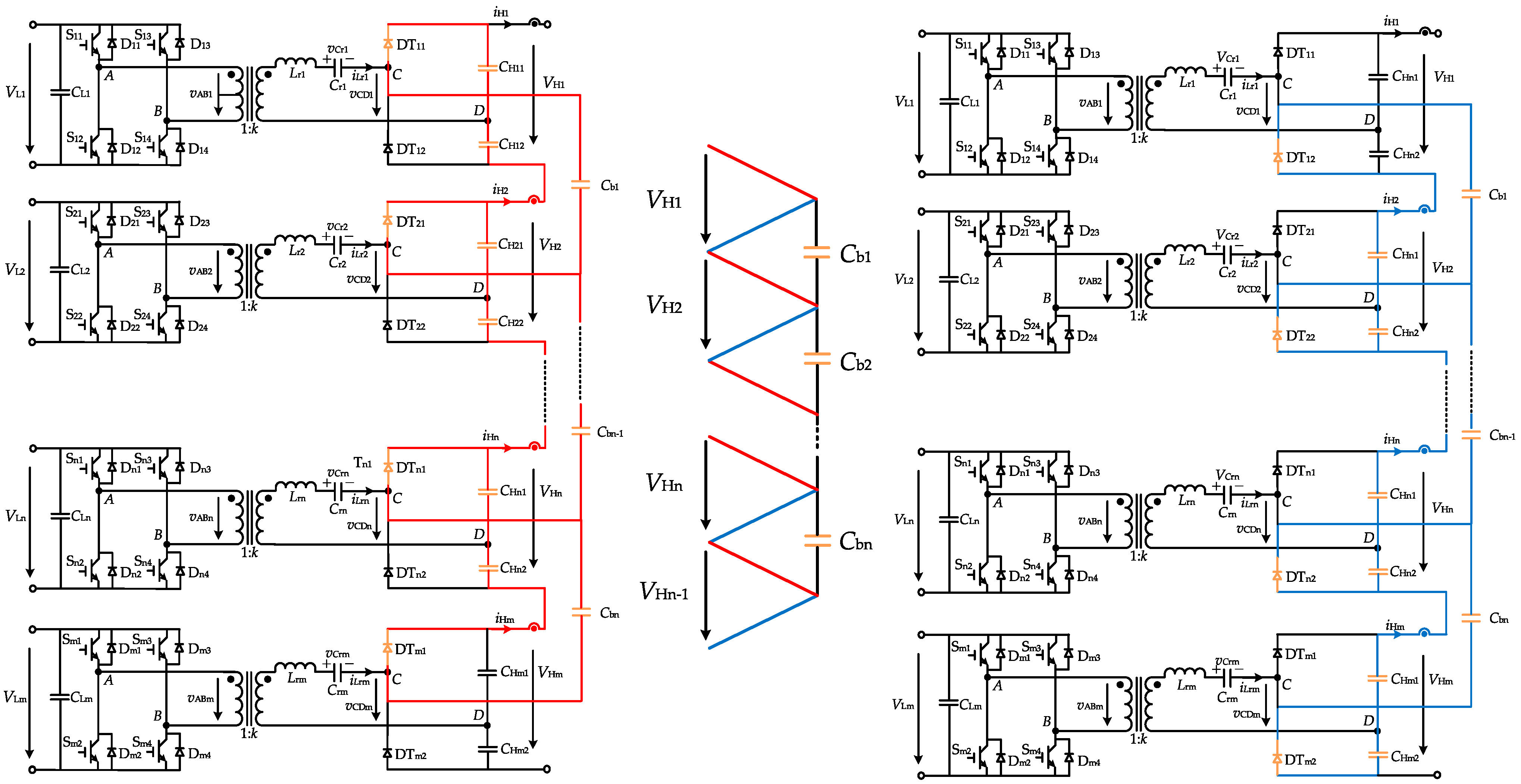
To reduce cost and enable power self-balancing, the high-voltage side incorporates a voltage-doubling rectifier network composed of diodes and capacitors. The topology of the proposed IIOS converter with a Self-Power-Balancing capacitor adopted in this paper is illustrated in Figure 2. The power-balancing capacitor establishes distinct current paths during the conduction of the upper and lower bridge arms. This configuration achieves power equilibrium among submodules. In power electronic converters, Pulse-Frequency Modulation (PFM) is well suited for wide-range power regulation, as it effectively reduces switching losses, improves efficiency, and suppresses electromagnetic interference (EMI). However, in the proposed topology, achieving power self-balancing among submodules requires a unified switching frequency across the total system. Phase-Shift Modulation (PSM) allows output voltage regulation through adjustment of phase-shift duty cycles without altering the system frequency. However, relying solely on PSM may compromise soft-switching conditions for the IGBTs. To address this issue, an innovative PFMT-PSMN hybrid control strategy is proposed. In this scheme, the total system switching frequency is regulated using PFM, while the phase-shift duty cycles of the n submodules are determined based on the soft-switching boundary conditions of the IGBTs and controlled via PSM. The PFMT-PSMN strategy enables simultaneous adjustment of the global switching frequency and the individual phase-shift duty cycles, ensuring soft-switching operation while minimizing the system switching frequency. Furthermore, the proposed method achieves effective power balancing within the converter. The effectiveness of the proposed topology and hybrid control strategy is verified through simulations conducted in the MATLAB/Simulink environment.

2. Proposed Topology and Operation

2.1. Topology Description

This paper analyzes a configuration using a full-bridge two-level topology on the low-voltage (LV) side and a half-bridge topology on the high-voltage (HV) side, as shown in Figure 2.
The system consists of m series-connected submodules. The nth submodule is selected as a representative to illustrate the operating principles. CLn refers to the LV capacitor, Sn1:Sn4 are LV side IGBTs (Dn1:Dn4 are anti-parallel diodes), and DTn1:DTn2 are HV side diodes. Lrn is the transformer leakage inductance, Crn is the resonant capacitor, the transformer ratio is 1:k, and CHn1 and CHn2 are the HV dividing capacitors. VLn is the input voltage on the low-voltage side, VHn is the input voltage on the high-voltage side, vCrn is the resonant capacitor voltage, iLrn is the resonant inductor current, vABn is the resonant tank input voltage, and vCDn is the resonant tank output voltage. Cbn is the power-balancing capacitor, vCbn is the power-balancing capacitor voltage, and iCbn is power-balancing capacitor current. VH is the total output voltage of the entire system, MFn is the voltage gain of the nth submodule. Output voltage balancing and energy transfer in series-connected DC/DC converter topologies are achieved through power-balancing capacitors.
Simultaneously, the proposed topology retains the capability for fault isolation. In the event of a failure in the nth submodule, the fault can be mitigated by turning off all switches on the submodule’s low-voltage side and disconnecting the balancing capacitor associated with the faulty submodule. Moreover, the topology can alleviate power deficiency resulting from the failure of an individual wind turbine through the incorporation of additional redundancy.

2.2. Operation Principle

Prior to theoretical analysis, define the switching frequency as fs, the switching period as Ts, and the resonant frequency as frn, the resonant angular frequency as ωrn, the characteristic impedance as Zrn, and the phase-shift duty cycle as Dn.
Z rn = L rn / C rn f rn = 1 2 π L rn C rn ω rn = 2 π f rn ,
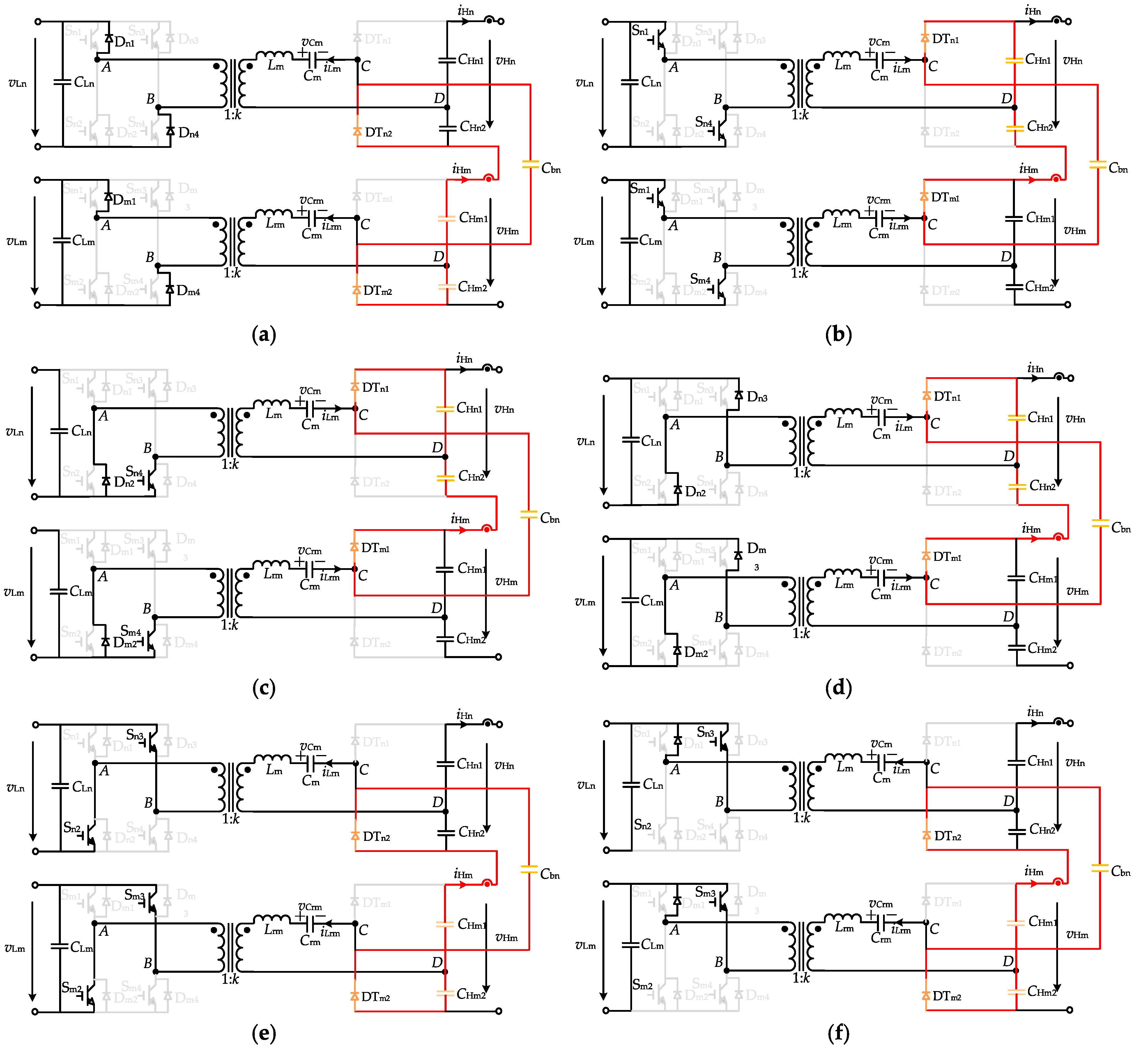
Figure 3 shows the trigger pulses of the proposed converter submodule, along with key waveforms of the power-balancing capacitor during steady-state operation. The converter operates in six distinct modes within each switching cycle. Here, VHn denotes the output voltage of the nth submodule. For analysis, it is assumed that the output voltage of the nth submodule exceeds that of the mth submodule; specifically, VHn > VHN > VHm, while the remaining submodules operate at the rated voltage VHN. The equivalent circuits corresponding to each operating mode are illustrated in Figure 4. Figure 3 illustrates the waveforms under relatively ideal conditions. However, due to the influence of magnetic components [30,31], the same power converter may exhibit different waveforms at varying voltage and power levels. For instance, VABn is typically accompanied by oscillations, which in turn affect other waveforms. In addition, iLrn and ucrn show ripples of varying magnitudes depending on the voltage level and operating frequency. This phenomenon should be carefully considered in practical applications, as it may influence the stability and efficiency of the system.
The operating principles and waveform characteristics of the mth submodule are analogous to those of the nth submodule. The following analysis focuses on:
  • Operation principles and waveforms of the nth submodule within the proposed DC/DC topology.
  • Energy transfer between the nth and mth submodules via the power-balancing capacitor Cbn.
Mode 1 (t0t1): As shown in Figure 4a. IGBT Sn4 receives trigger signals. Switch Sn3 hard switches off, while switch Sn1 stays active. The negative leakage inductance current iLr initiates freewheeling through diodes Dn1 and Dn4 on the low-voltage side. This clamps the voltage across switches Sn1 and Sn4 to zero, enabling zero-voltage switching (ZVS) to turn on. On the high-voltage side, capacitors CHn2 charge. Conducting diodes DTn2 and DTm2 form a closed loop with power-balancing capacitor Cbn, enabling Cbn to discharge into CHm1 and CHm2. The time-domain relationships for the inductor and capacitor are defined as:
Z rn i Ln ( t t 0 ) v cn ( t t 0 ) = cos ω rn ( t t 0 ) sin ω rn ( t t 0 ) sin ω rn ( t t 0 ) cos ω rn ( t t 0 ) Z rn i Ln ( t 0 ) v cn ( t 0 ) + sin ω rn ( t t 0 ) 1 cos ω rn ( t t 0 ) ( k V Ln + V Hn 2 ) i cb ( t t 0 ) v cb ( t t 0 ) = 0 m + 1 2 k V H n C bn sin ω o ( t t 0 ) cos ω o ( t t 0 ) ( m n ) V Hm ,
Mode 2 (t1t2): As shown in Figure 4b. At t1, the leakage inductance current iLr crosses zero from negative to positive enabling ZVS turn-on of switching devices Sn1 and Sn4. Simultaneously, the application of reverse voltage forces DTn2 and DTm2 to be turned off. The available turn-off period spans half the switching cycle. High-voltage capacitors CHn1 charge. With Diodes DTn1 and DTm1 conducting, nth submodule capacitors CHn1 and CHn1 and power-balancing capacitor Cbn form a closed loop enabling CHn1 and CHn2 to discharge into Cbn. The time-domain relationships for the inductor and capacitor are defined as:
Z rn i Ln ( t t 1 ) v cn ( t t 1 ) = sin ω rn ( t t 1 ) cos ω rn ( t t 1 ) v cn ( t 1 ) + sin ω rn ( t t 1 ) 1 cos ω rn ( t t 1 ) ( k V Ln V Hn 2 ) i cb ( t t 1 ) v cb ( t t 1 ) = 0 m + 1 2 k V H n C bn sin ω o ( t t 1 ) cos ω o ( t t 1 ) ( m n ) V Hn ,
Mode 3 (t2t3): As shown in Figure 4c. At time t2, switch Sn1 turns off under hard-switching conditions, while Sn2 receives its trigger signal. Switch Sn4 remains conducting. The positive leakage inductance current iLr directs the low-voltage-side current through Sn4 and diode Dn2. High-voltage capacitors CHn1 charge. Diodes Tn1 and Tm1 remain conducting on the high-voltage side. A discharge path persists between high-voltage capacitors CHn1/CHn2 and power-balancing capacitor Cbn, enabling CHn1 and CHn2 to discharge into Cbn. The time-domain relationships for the inductor and capacitor are defined as:
Z rn i Ln ( t t 2 ) v cn ( t t 2 ) = cos ω rn ( t t 2 ) sin ω rn ( t t 2 ) sin ω rn ( t t 2 ) cos ω rn ( t t 2 ) Z rn i Ln ( t 2 ) v cn ( t 2 ) + sin ω rn ( t t 2 ) 1 cos ω rn ( t t 2 ) ( V Hn 2 ) i cb ( t t 2 ) v cb ( t t 2 ) = 0 m + 1 2 k V H n C bn sin ω o ( t t 2 ) cos ω o ( t t 2 ) ( m n ) V Hn ,
Mode 4 (t3t4): As shown in Figure 4d. At time t3, IGBT Sn3 received trigger signals. Switch Sn4 hard switches off, while switch Sn2 stays active. The positive leakage inductance current iLr initiates freewheeling through diodes Dn2 and Dn3 on the low-voltage side. This clamps the voltage across switches Sn2 and Sn3 to zero, enabling zero-voltage switching (ZVS) to turn on. High-voltage capacitors CHn1 charge. A discharge path persists between high-voltage capacitors CHn1/CHn2 and power-balancing capacitor Cbn, enabling CHn1 and CHn2 to discharge into Cbn. The time-domain relationships for the inductor and capacitor are defined as:
Z rn i Ln ( t t 3 ) v cn ( t t 3 ) = cos ω rn ( t t 3 ) sin ω rn ( t t 3 ) sin ω rn ( t t 3 ) cos ω rn ( t t 3 ) Z rn i Ln ( t 3 ) v cn ( t 3 ) + sin ω rn ( t t 3 ) 1 + cos ω rn ( t t 3 ) ( k V Ln + V Hn 2 ) i cb ( t t 3 ) v cb ( t t 3 ) = 0 m + 1 2 k V H n C bn sin ω o ( t t 3 ) cos ω o ( t t 3 ) ( m n ) V Hn ,
Mode 5 (t4t5): As shown in Figure 4e. At time t4, the leakage inductance current iLr crosses zero from positive to negative enabling the ZVS turn-on of switching devices Sn2 and Sn3. Simultaneously, reverse voltage application forces DTn1 and DTm1 to turn off. The available turn-off period spans half the switching cycle. High-voltage capacitors CHn2 charge. With diodes Tn2 and Tm2 conducting, nth submodule capacitors CHm2 and CHm2 and power-balancing capacitor Cbn form a closed loop, enabling Cbn to discharge into CHm2 and CHm2. The time-domain relationships for the inductor and capacitor are defined as:
Z rn i Ln ( t t 4 ) v cn ( t t 4 ) = sin ω rn ( t t 4 ) cos ω rn ( t t 4 ) v cn ( t 4 ) + sin ω rn ( t t 4 ) 1 + cos ω rn ( t t 4 ) ( k V Ln V Hn 2 ) i cb ( t t 4 ) v cb ( t t 4 ) = 0 m + 1 2 k V H n C bn sin ω o ( t t 4 ) cos ω o ( t t 4 ) ( m n ) V Hm ,
Mode 6 (t5t6): As shown in Figure 4f. At time t5, switch Sn2 turns off under hard-switching conditions, while Sn1 receives its trigger signal. Switch Sn3 remains conducting. The negative leakage inductance current iLr directs the low-voltage-side current through Sn3 and diode Dn1. High-voltage capacitors CHn2 charge. Diodes DTn2 and DTm2 remain conducting on the high-voltage side. A discharge path persists between high-voltage capacitors CHm1/CHm2 and power-balancing capacitor Cbn, enabling Cbn to discharge into CHn1 and CHn2. The time-domain relationships for the inductor and capacitor are defined as:
Z rn i Ln ( t t 5 ) v cn ( t t 5 ) = cos ω rn ( t t 5 ) sin ω rn ( t t 5 ) sin ω rn ( t t 5 ) cos ω rn ( t t 5 ) Z rn i Ln ( t 5 ) v cn ( t 5 ) + sin ω rn ( t t 5 ) 1 + cos ω rn ( t t 5 ) ( V Hn 2 ) i cb ( t t 5 ) v cb ( t t 5 ) = 0 m + 1 2 k V H n C bn sin ω o ( t t 5 ) cos ω o ( t t 5 ) ( m n ) V Hm ,

2.3. Power Balancing Principle

The proposed topology achieves inherent power balancing by enforcing a unified operating frequency across all submodules. Figure 5 illustrates the power self-balancing mechanism of the proposed IIOS topology with integrated power-balancing capacitors. When the upper arm on the high-voltage side is turned on, the balancing capacitor forms a current loop with the output capacitor of the preceding submodule. When the lower arm is turned on, it connects with the output capacitor of the subsequent submodule. Alternating the conduction of the upper and lower arms enables effective power transfer among cascaded submodules.

2.4. Soft-Switching Implementation

Ref. [32] established the boundary conditions required to maintain IGBT soft-switching operation over the full power range. For series resonant converters, achieving zero-voltage switching (ZVS) for IGBTs is critical to minimizing switching losses. However, ZVS is conditional; it requires the IGBT output capacitance to be fully charged or discharged within the designated dead time. Between the two bridge legs, soft switching is more difficult to achieve in the lagging leg than in the leading leg.
Idt is defined as the minimum current required to charge or discharge the output capacitance within the dead time. Given the short duration of the dead time, the current can be approximated as a constant current source during this interval. Accordingly, the ZVS boundary condition for the IGBTs and the expression for Idt are given by Equation (7).
Defining the rated power of Submodule n as PNn and the rated voltage as VNn and neglecting the reactive components in the system, the rated current is INn.
i Lrn t 0 I Nn = I dt k I Nn , I dt = 2 C oss V Ln t d , I Nn = P Nn V Nn ,
Coss denotes the output capacitance of the IGBTs, and td is the dead time.
iLrn(t0) = 0 represents the ideal case where the effect of output capacitance is neglected, while iLrn(t0) = −0.1INn accounts for the capacitive effect. The threshold value of 0.1 is considered the minimum normalized current required to achieve ZVS for the IGBTs. At a fixed positive voltage gain, the phase-shift duty cycle corresponding to the ZVS boundary decreases as the switching frequency increases.

2.5. Performance Comparison with Other IIOS Converters

Taking Table 1 as an example, the proposed topology is compared with mainstream power-balancing methods in terms of switching loss, control complexity, cost, and dynamic response. On the low-voltage side, the proposed topology employs a full-bridge structure with IGBTs to enable both frequency and phase control. On the high-voltage side, a voltage-doubling rectifier network composed of diodes and output capacitors is adopted to minimize the switching cost. The balancing circuit relies solely on a single balancing capacitor to achieve power balancing, thereby significantly reducing the number of switching devices compared with the schemes in [26,28,29]. In [26,28], additional control circuits are also required.
The proposed PFMT-PSMN control strategy further lowers switching frequency, thereby reducing losses and ripple. Although the self-balancing mechanism yields a slightly slower response than [26,28], simulations confirm its capability to achieve stable power balancing. Compared with the LC resonant self-balancing in [29], direct DC energy transfer in the proposed topology reduces losses and improves response.
In conclusion, the proposed topology demonstrates clear cost advantages, simplifies control through self-balancing, and, with PFMT-PSMN, achieves reduced switching loss and enhanced dynamic performance.

3. PFMT-PSMN Hybrid Control Strategy for Proposed Topology and Simulation

3.1. PFMT-PSMN Hybrid Control Strategy

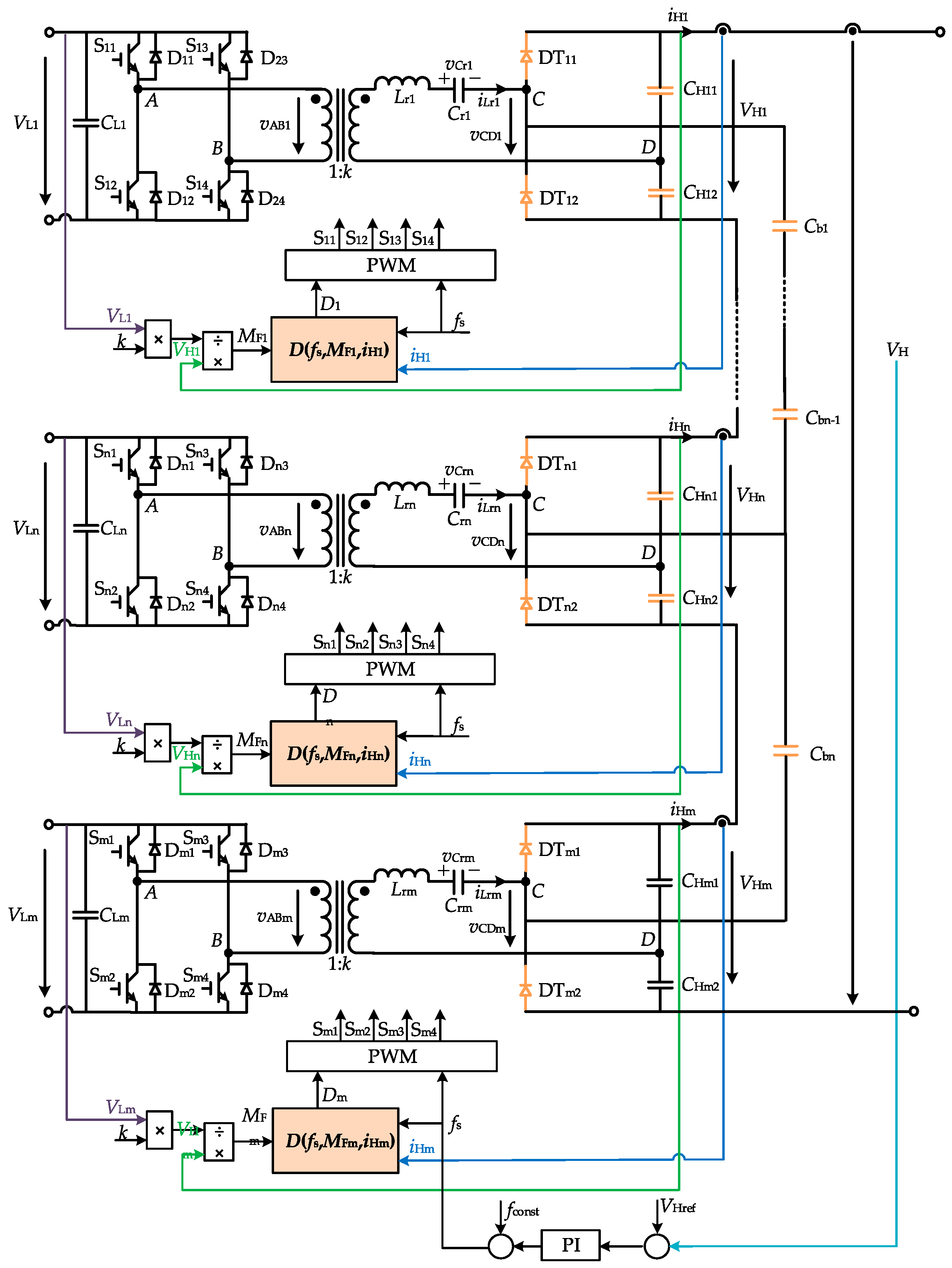
Building on this approach, this paper presents an improved control strategy tailored to the proposed power-balancing circuit. The total output voltage is regulated using Pulse-Frequency Modulation (PFM), while the optimal phase-shift duty cycle for each of the n submodules is calculated based on the switching frequency determined by the PFM stage. The enhanced method is defined as the PFMT-PSMN hybrid control strategy.
This approach enhances converter efficiency while limiting the variation range of the switching frequency. The proposed topology requires the precise synchronization of the switching frequency across all m submodules. An optimized soft-switching control strategy determines the optimal phase-shift duty cycle for each submodule, enabling system-wide performance improvement.
The analytic expression for Dn (fs, MFn, iHn) and fsn is obtained as:
D n f s , M Fn , i Hn = 1 2 B f s π f rn Δ D           M Fn = V Hn k V Ln B = tan 1 A + sin 1 M Fn 1 1 + A 2 sin π f rn 2 f s + A 1 + A 2 cos π f rn 2 f s A = I d t k π f rn f s 1 M Fn 2
td is the dead time, and ΔD represents the design margin introduced to ensure ZVS, accounting for approximation errors and neglecting the influence of dead time, and MF is the voltage gain.

3.2. PFMT-PSMN Hybrid Control for Proposed Topology

Figure 6 illustrates the control block diagram of the PFMT-PSMN hybrid control strategy. The system generates an error signal by subtracting the measured input/output voltage from its reference value, enabling voltage regulation (input or output) while maintaining forward power transfer. An empirical feedforward term fconst is summed with the PI compensatory output to determine the switching frequency fs, thereby improving dynamic response and suppressing oscillation. The phase-shift duty cycle Dn is calculated via the function Dn (fs, MFn, iHn). This architecture achieves coordinated PFMT-PSMN hybrid control with adaptive parameter adjustment.

4. Simulation Results

4.1. Simulation Parameters

Table 2 summarizes key simulation parameters. The proposed converter operates at a resonant frequency of 4 kHz across all submodules. The power-balancing capacitance is set to 0.1 mF (one-tenth of the high-voltage-side output capacitance), as excessive capacitance prolongs balancing time while insufficient capacitance fails to achieve power balance. The system input power, constrained by the source characteristics, has a rated power PN and rated voltage VN; the system operates under PFMT-PSMN hybrid control.

4.2. Simulation Results of PFMT-PSMN Hybrid Control

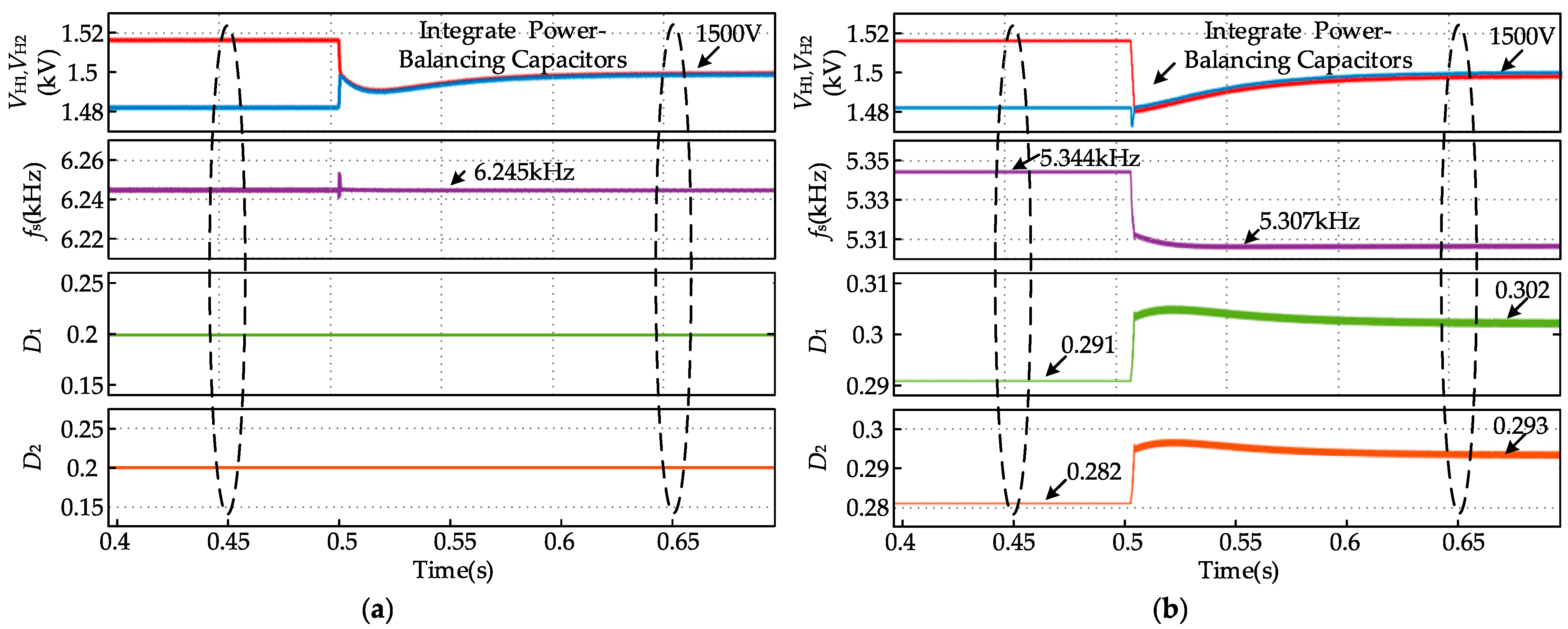
Figure 7a,b compare two control strategies: conventional PFM control and a hybrid PFMT-PSMN control approach. Since this section focuses on control strategy verification through simulation, two proposed DC/DC topologies are connected in series, and power balancing is achieved via power-balancing capacitors. Under series connection, identical output currents from both converters imply that equal output voltages correspond to balanced power. Regardless of the control method, the system consistently maintains a total output voltage of 3 kV and achieves power balancing, with each converter delivering 180 kW.
As shown in Figure 7b, the switching frequency before power balancing under hybrid PFMT-PSMN control is 5.344 kHz and 5.307 kHz after balancing—both significantly lower than the 6.245 kHz observed with conventional PFM control. This reduction in switching frequency through hybrid PFMT-PSMN control facilitates device selection and simplifies magnetic component design.
In Figure 7b, the phase-shift duty cycle of Topology 1 changes from 0.291 before voltage balancing to 0.302 after, while that of Topology 2 shifts from 0.282 to 0.293. This demonstrates that the hybrid PFMT-PSMN control modifies the phase-shift duty cycles of both topologies. Since the input powers of the two converters differ, their duty cycles naturally vary according to Equation (8). By introducing an additional control variable, phase-shift duty cycle—alongside switching frequency—the hybrid control strategy increases the system’s control flexibility. This decoupling of voltage regulation from frequency alone significantly reduces the required switching frequency and simplifies the realization of soft switching across the system.
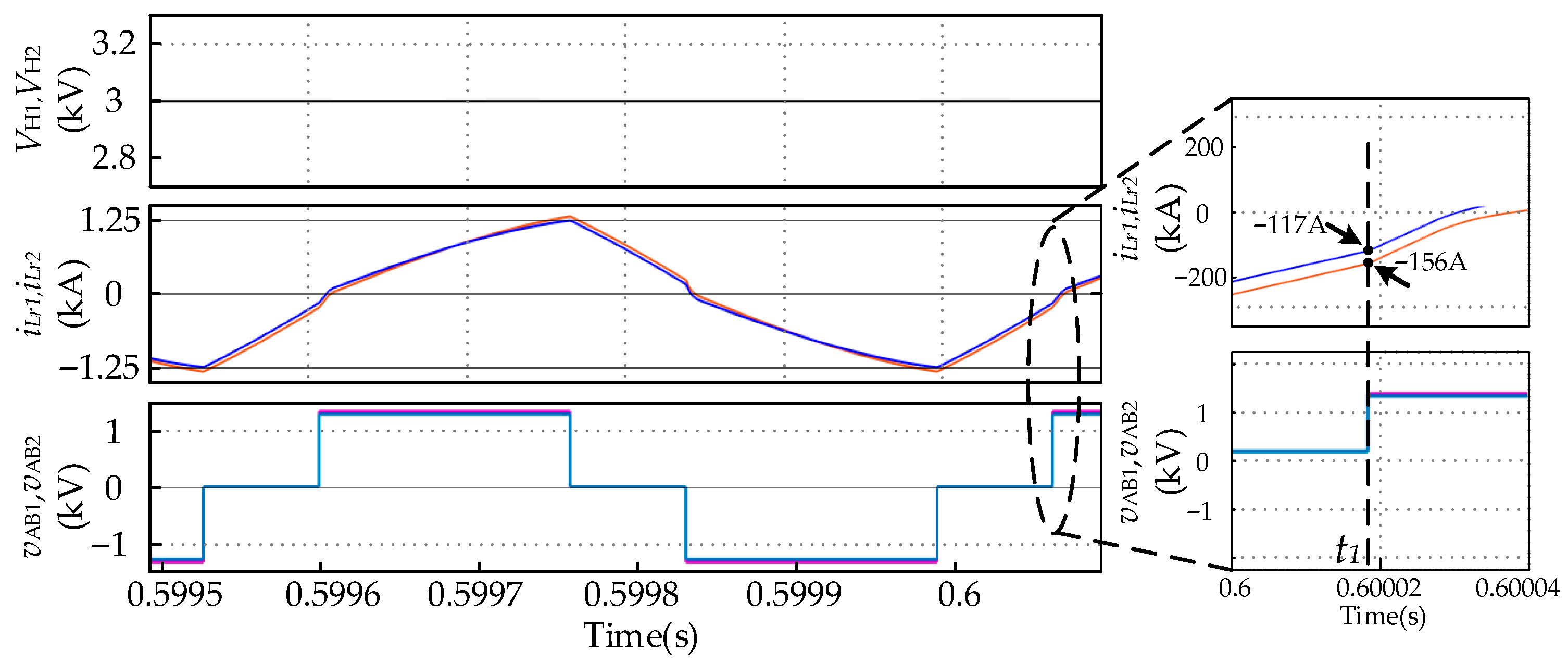
Figure 8 presents the steady-state waveforms at 0.6 s from Figure 7b, during which the total output voltage remains at 3 kV. As shown, the resonant currents at time t1 are −127 A and −156 A for the two topologies, respectively, while the actual value of Isw/k is −134 A. This indicates that the system operates near the boundary of soft switching, enabling zero-voltage switching (ZVS) turn-on for the IGBTs.

4.3. Simulation Results of the Operating Characteristics of Series-Connected Submodules and the Power-Balancing Capacitor

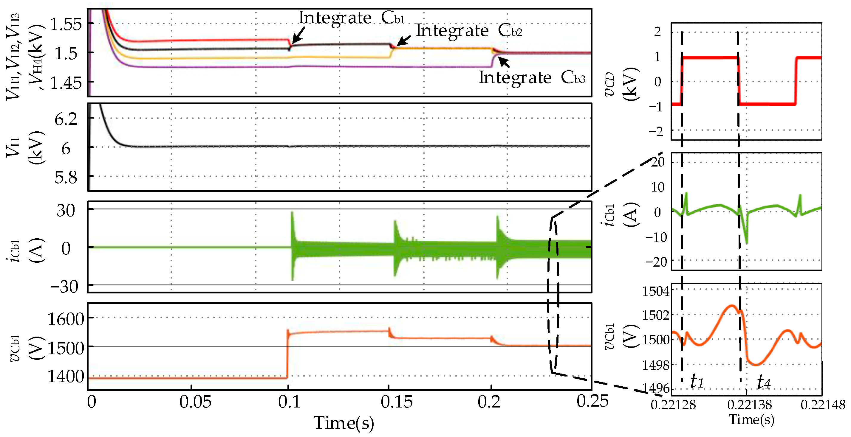
To verify the operating principle illustrated in Figure 2, four proposed converter topologies were connected in series, and power balancing among different submodules was achieved using three power-balancing capacitors. As shown in Figure 9, at t = 0.1 s, power-balancing capacitor Cb1 is connected, enabling power balancing between Submodules 1 and 2, while the output voltages of Submodules 3 and 4 remain nearly unchanged. At t = 0.15 s, Cb2 is introduced, extending power balancing to Submodules 1–3. Finally, at t = 0.2 s, Cb3 is connected, achieving power balancing across the entire series-connected system.
During the connection of each balancing capacitor, the total output voltage remains constant at 6 kV under hybrid PFMT-PSMN control. The right-hand plot in Figure 9 shows the voltage and current waveforms of capacitor Cb1 at a steady state. At time t1, the upper bridge of the high-voltage side is conducting, allowing CH11/CH12 of Submodule 1 to discharge into Cb1, resulting in a voltage rise across the capacitor. At t4, the lower bridge conducts, and Cb1 discharges into CH21/CH22, causing the capacitor voltage to decrease. The waveforms of the other balancing capacitors follow the same principle.
By alternating conduction of the upper and lower bridge arms, the power-balancing capacitor serves as an energy transfer bridge between CHn1/CHn2, ensuring uniform output voltages across all submodules. Consequently, the voltage stress on the high-voltage switches of each submodule is equalized. The integration of power-balancing capacitors thus contributes to protecting the high-voltage-side switching devices in each submodule.

5. Conclusions

This paper addresses the output power balancing challenge in offshore wind DC aggregation systems caused by power fluctuations. A novel series-connected DC aggregation topology incorporating power self-balancing capacitors is proposed to enable energy equalization among submodules. Based on soft-switching boundary conditions, a PFMT-PSMN hybrid control strategy is proposed that simultaneously regulates the phase-shift duty cycle and switching frequency. The main contributions of this work are summarized as follows:
  • A series-connected DC aggregation topology incorporating power-balancing capacitors is proposed. The working principles of the balancing capacitor and the resonant components are analyzed using time-domain methods.
  • Based on soft-switching boundary constraints, conventional PFM and PSM methods are refined and a PFMT-PSMN hybrid control strategy is proposed. This strategy enables simultaneous adjustment of the switching frequency and phase-shift duty cycle, achieving soft-switching operation while reducing the switching frequency. It is well suited for series-connected DC aggregation topologies with power self-balancing capacitors. The PFMT-PSMN control method adopted in this paper requires real-time monitoring of multiple parameters (voltage, current, and gain), which may increase the control cost; however, it can be appropriately simplified for practical applications.
  • The effectiveness of the proposed power-balancing topology and PFMT-PSMN control strategy is verified through MATLAB/Simulink simulations. A hardware prototype is currently under design, and future work will involve experimental validation to further corroborate the theoretical analysis and simulation results presented in this paper.
The proposed strategy introduces a higher degree of control freedom, significantly reducing switching losses. The self-balancing topology provides a feasible solution to output voltage imbalance caused by power instability in series-connected aggregation systems. This approach is also applicable to other fully DC aggregation and transmission systems in renewable energy generation.

Author Contributions

Conceptualization, H.L. and Q.X.; methodology, H.L.; software, H.L.; validation, Q.X., R.H. and Q.L.; formal analysis, H.L.; investigation, H.L.; resources, Q.L.; data curation, R.H.; writing—original draft preparation, H.L.; writing—review and editing, H.L.; visualization, Q.X.; supervision, Q.L.; project administration, Q.X.; funding acquisition, Q.L. All authors have read and agreed to the published version of the manuscript.

Funding

This research was funded by Digital Grid Research Foundation of China Southern Power Grid, grant number DPGCSG-2024-KF-08.

Conflicts of Interest

The authors declare no conflict of interest.

References

  1. Li, B.; Liu, J.; Wang, Z.; Zhang, S.; Xu, D. Modular High-Power DC–DC Converter for MVDC Renewable Energy Collection Systems. IEEE Trans. Ind. Electron. 2021, 68, 5875–5886. [Google Scholar] [CrossRef]
  2. Meyer, C.; Hoing, M.; Peterson, A.; De Doncker, R.W. Control and Design of DC Grids for Offshore Wind Farms. IEEE Trans. Ind. Appl. 2007, 43, 1475–1482. [Google Scholar] [CrossRef]
  3. Jiao, Z.; Sun, J.; Yao, X.; Le, Y.; Chen, J.; Wang, A. Lightning Overvoltage Simulation and Design of a Novel Surge Protective Device for High-Power Offshore Wind Farms. IEEE Trans. Power Deliv. 2024, 39, 2306–2316. [Google Scholar] [CrossRef]
  4. Xiao, H.; Huang, X.; Huang, Y.; Liu, T.; Yang, P. Black Start Strategy of DRU-Based Low-Frequency AC Transmission System for Offshore Wind Power Integration. IEEE Trans. Ind. Appl. 2024, 60, 8319–8328. [Google Scholar] [CrossRef]
  5. Hassan Zamani, M.; Hossein Riahy, G.; Abedi, M. Rotor-Speed Stability Improvement of Dual Stator-Winding Induction Generator-Based Wind Farms by Control-Windings Voltage Oriented Control. IEEE Trans. Power Electron. 2016, 31, 5538–5546. [Google Scholar] [CrossRef]
  6. Ning, G.; Du, L.; Yuan, L.; Sun, Y.; Liu, Y.; Xu, G.; Han, H.; Su, M. Single-Stage IIOS Converter with Auto-Voltage-Sharing for Distributed Photovoltaic MVDC Collection System. IEEE Trans. Power Electron. 2024, 39, 14172–14178. [Google Scholar] [CrossRef]
  7. Bui, D.-V.; Cha, H.; Nguyen, C.V. Asymmetrical PWM Scheme Eliminating Duty Cycle Limitation in Input-Parallel Output-Series DC–DC Converter. IEEE Trans. Power Electron. 2022, 37, 2485–2490. [Google Scholar] [CrossRef]
  8. Fang, T.; Ruan, X.; Tse, C.K. Control Strategy to Achieve Input and Output Voltage Sharing for Input-Series–Output-Series-Connected Inverter Systems. IEEE Trans. Power Electron. 2010, 25, 1585–1596. [Google Scholar] [CrossRef]
  9. Shi, J.; Zhou, L.; He, X. Common-Duty-Ratio Control of Input-Parallel Output-Parallel (IPOP) Connected DC–DC Converter Modules with Automatic Sharing of Currents. IEEE Trans. Power Electron. 2012, 27, 3277–3291. [Google Scholar] [CrossRef]
  10. Wang, Z.; Li, Z.; Zhang, Y.; Shu, J.; Liu, J.; Li, X. Unified Modeling and Control Methods for Ripple Power Decoupling Circuit Based on DC-Split Capacitor. IEEE Trans. Power Electron. 2025, 40, 665–678. [Google Scholar] [CrossRef]
  11. Vazquez, A.; Rodriguez, A.; Lamar, D.G.; Hernando, M.M. Advanced Control Techniques to Improve the Efficiency of IPOP Modular QSW-ZVS Converters. IEEE Trans. Power Electron. 2018, 33, 73–86. [Google Scholar] [CrossRef]
  12. Xia, Y.; Yu, M.; Zhang, Y.; Lv, Z.; Wei, W. Decentralized Suppression Strategy of Circulating Currents Among IPOP Single-Phase DC/AC Converters. IEEE J. Emerg. Sel. Top. Power Electron. 2020, 8, 1571–1583. [Google Scholar] [CrossRef]
  13. Sun, K.; Su, M.; Xu, G.; Chen, X.; Xiong, W. Modulated Coupled Inductor-Based IPOP-DAB Converter with Optimized Modulation Trajectory Considering the Phase-Shift Angle Between Submodules for SST Applications. IEEE J. Emerg. Sel. Top. Power Electron. 2023, 11, 6112–6123. [Google Scholar] [CrossRef]
  14. Zhuang, Y.; Liu, F.; Huang, W.; Wang, S.; Jiang, J.; Pan, S.; Zha, X. A Peak Current Reducing Method for Input-Independent and Output-Series Modular Converters with LC-Branch-Based Power Balancing Unit. IEEE Trans. Ind. Electron. 2023, 70, 418–429. [Google Scholar] [CrossRef]
  15. Wei, C.; Zhu, X.; Jin, K.; Wu, Y. Modular Multiport Voltage Balance Topology Based on Boost Half-Bridge and Quadruple Semiactive Rectifier for MVdc Integration of Distributed PVs. IEEE J. Emerg. Sel. Top. Power Electron. 2025, 13, 3147–3161. [Google Scholar] [CrossRef]
  16. Zhu, X.; Liu, L.; Jin, K.; Zhang, B. Current-Fed Multiactive Bridge Converter with Inherently Output Voltage Balance for Distributed Photovoltaics MVDC Integration. IEEE Trans. Ind. Electron. 2025, 72, 2563–2575. [Google Scholar] [CrossRef]
  17. Zhuang, Y.; Zhang, Y.; Chen, X.; Zhu, H.; Huang, Y.; Liu, F. A Novel Fault-Tolerant Topology for MVDC Grids Interface of Photovoltaic Generation Systems. IEEE Trans. Ind. Electron. 2025, 72, 547–558. [Google Scholar] [CrossRef]
  18. Chen, W.; Wang, G. Decentralized Voltage-Sharing Control Strategy for Fully Modular Input-Series–Output-Series System with Improved Voltage Regulation. IEEE Trans. Ind. Electron. 2015, 62, 2777–2787. [Google Scholar] [CrossRef]
  19. Kuperman, A. Simple Enhancement of Series–Series-Compensated Inductive Wireless Power Transfer Links Operating with Load-Independent Voltage Output at Fixed Frequency to Attain Zero Inverter Phase Angle. IEEE Trans. Power Electron. 2023, 38, 5670–5674. [Google Scholar] [CrossRef]
  20. Chen, W.; Wang, G.; Ruan, X.; Jiang, W.; Gu, W. Wireless Input-Voltage-Sharing Control Strategy for Input-Series Output-Parallel (ISOP) System Based on Positive Output-Voltage Gradient Method. IEEE Trans. Ind. Electron. 2014, 61, 6022–6030. [Google Scholar] [CrossRef]
  21. Liu, Y.; Hu, H.; Wang, X.; Gang, Y.; Li, Y. Voltage Balance Scheme for Input-Series Output-Series DAB DC–DC Converter with Bidirectional Power Flow. IEEE Trans. Power Electron. 2024, 39, 12030–12034. [Google Scholar] [CrossRef]
  22. Ma, D.; Chen, W.; Ruan, X. A Review of Voltage/Current Sharing Techniques for Series–Parallel-Connected Modular Power Conversion Systems. IEEE Trans. Power Electron. 2020, 35, 12383–12400. [Google Scholar] [CrossRef]
  23. Barzegarkhoo, R.; Farhangi, M.; Lee, S.S.; Aguilera, R.P.; Blaabjerg, F.; Siwakoti, Y.P. A Novel Active Neutral Point-Clamped Five-Level Inverter with Single-Stage-Integrated Dynamic Voltage Boosting Feature. IEEE Trans. Power Electron. 2023, 38, 7796–7809. [Google Scholar] [CrossRef]
  24. Sun, L.; Wang, F.; Zhuo, F.; Zhu, T. Multi-Modular Cascaded Phase-Shifted Full-Bridge Converter for DC Grid Connection of Large-Scale Photovoltaic Power Systems. In Proceedings of the 2016 IEEE 8th International Power Electronics and Motion Control Conference (IPEMC-ECCE Asia), Hefei, China, 22–26 May 2016; pp. 1561–1565. [Google Scholar]
  25. Liu, Y.; Abu-Rub, H.; Ge, B. Front-End Isolated Quasi-Z-Source DC–DC Converter Modules in Series for High-Power Photovoltaic Systems—Part I: Configuration, Operation, and Evaluation. IEEE Trans. Ind. Electron. 2017, 64, 347–358. [Google Scholar] [CrossRef]
  26. Huang, Y.; Liu, F.; Zhuang, Y. Bidirectional Buck-Boost and Series LC-Based Power Balancing Units for Photovoltaic DC Collection System. IEEE J. Emerg. Sel. Top. Power Electron. 2021, 9, 6726–6738. [Google Scholar] [CrossRef]
  27. Li, X.; Zhu, M.; Su, M.; Ma, J.; Li, Y.; Cai, X. Input-Independent and Output-Series Connected Modular DC–DC Converter with Intermodule Power Balancing Units for MVdc Integration of Distributed PV. IEEE Trans. Power Electron. 2020, 35, 1622–1636. [Google Scholar] [CrossRef]
  28. Rong, F.; Wu, G.; Li, X.; Huang, S.; Zhou, B. ALL-DC Offshore Wind Farm with Series-Connected Wind Turbines to Overcome Unequal Wind Speeds. IEEE Trans. Power Electron. 2019, 34, 1370–1381. [Google Scholar] [CrossRef]
  29. Zhuang, Y.; Liu, F.; Huang, Y.; Liu, P.; Zhang, B. A Multiport Modular DC–DC Converter with Low-Loss Series LC Power Balancing Unit for MVDC Interface of Distributed Photovoltaics. IEEE Trans. Power Electron. 2021, 36, 7736–7749. [Google Scholar] [CrossRef]
  30. Hilal, A.; Raulet, M.-A.; Martin, C.; Sixdenier, F. Power Loss Prediction and Precise Modeling of Magnetic Powder Components in DC–DC Power Converter Application. IEEE Trans. Power Electron. 2015, 30, 2232–2238. [Google Scholar] [CrossRef]
  31. Imaoka, J.; Okamoto, K.; Shoyama, M.; Ishikura, Y.; Noah, M.; Yamamoto, M. Modeling, Magnetic Design, Simulation Methods, and Experimental Evaluation of Various Powder Cores Used in Power Converters Considering Their DC Superimposition Characteristics. IEEE Trans. Power Electron. 2019, 34, 9033–9051. [Google Scholar] [CrossRef]
  32. Wang, C.; Wang, H.; Zhang, T. Hybrid Four-Quadrant DC–DC Converter for DC Wind Farm Collection Systems. J. Power Electron. 2024, 24, 42–54. [Google Scholar] [CrossRef]
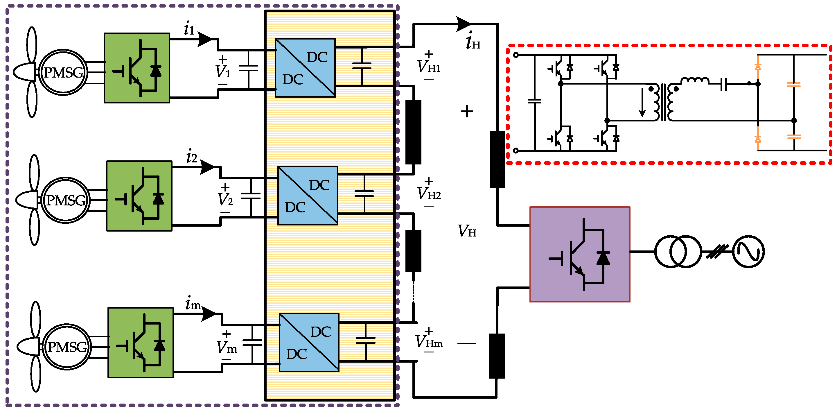
Figure 1. Fully DC aggregation topology for offshore wind power transmission.
Electronics 14 03422 g001
Figure 2. Topology of the proposed IIOS converter with a Self-Power-Balancing capacitor.
Electronics 14 03422 g002
Figure 3. Key waveforms of the proposed converter during steady-state operation.
Electronics 14 03422 g003
Figure 4. Equivalent circuits for different operating modes: (a) t0t1, (b) t1t2, (c) t2t3, (d) t3t4, (e) t4t5 (f) t5t6.
Electronics 14 03422 g004
Figure 5. Power-balancing principle of the proposed IIOS converter with a power-balancing capacitor.
Electronics 14 03422 g005
Figure 6. PFMT-PSMN hybrid control for proposed topology.
Electronics 14 03422 g006
Figure 7. Key waveforms of the proposed converter topology during power-balancing capacitor activation at t = 0.5 s. (a) PFM control. (b) PFMT-PSMN hybrid control.
Electronics 14 03422 g007
Figure 8. Key waveforms of the proposed converter topology under steady-state conditions after power-balancing capacitor integration.
Electronics 14 03422 g008
Figure 9. Key waveforms of the proposed converter topology during stepwise activation of series-connected power-balancing capacitors.
Electronics 14 03422 g009
Table 1. Performance comparison with other IIOS converters.
Proposed
Converter
PSFB + Buck-Boost
Converter [26]
PSFB + Buck-Boost + Phase-Shift LC Solution [28]DAB +
Self-Balancing
LC Solution [29]
Semiconductor
device
4m IGBTs
and 2m Diodes
4m + 2(m − 1)
IGBTs and
2m Diodes
4m + 2(m − 1)
IGBTs and
2m Diodes
8m IGBTs
Additionally
circuits
(m − 1) capacitor
circuits
2(m−1) Buck-Boost circuits2(m − 1) Buck-Boost and LC circuits(m − 1) LC
circuits
Control loop m2m − 12m − 1m
Implementation and control complexitySimpleComplexVery ComplexSimple
Input
ripple
LowLargeLargeLarge
CostVery LowHighVery HighHigh
Dynamic responseSlightly SlowFastVery FastSlow
Switching lossLowLargeLargeLow
Table 2. Simulation parameters.
ParametersValuesParametersValues
Output power Pout360 kWTransformer ratio 1:k1:2.2
Resonant frequency fr4 kHzRated voltage VHN1.5 kV
Commutation turn-off time tc-off50 μsResonant inductance
Lrn
400 µH
Resonant capacitance Crn4 µFDead time td1 µs
The high-voltage capacitors CHn1/CHn21 mFPower-balancing capacitor Cbn0.1 mF
Disclaimer/Publisher’s Note: The statements, opinions and data contained in all publications are solely those of the individual author(s) and contributor(s) and not of MDPI and/or the editor(s). MDPI and/or the editor(s) disclaim responsibility for any injury to people or property resulting from any ideas, methods, instructions or products referred to in the content.