Article

A DC-Link Current Pulsation Compensator Based on a Triple-Active Bridge Converter Topology

1
Faculty of Electrical Engineering and Computer Science, Lublin University of Technology, 20-618 Lublin, Poland
2
Faculty of Electrical Engineering, Warsaw University of Technology, 00-661 Warsaw, Poland
*
Author to whom correspondence should be addressed.
Electronics 2025, 14(16), 3196; https://doi.org/10.3390/electronics14163196
Submission received: 9 July 2025 / Revised: 6 August 2025 / Accepted: 10 August 2025 / Published: 11 August 2025

Abstract

This paper presents a method of compensating the AC pulsation appearing in the DC-link of a four-wire AC/DC converter operating with asymmetric output currents. If such a converter is operating with an electrochemical energy storage system, the AC component can cause several issues for the battery. In order to solve this problem, a DC/DC converter is used to redirect the AC component into a capacitor bank. The triple-active bridge (TAB) converter is selected for this purpose. The converter is modeled using a reduced-order modelling approach, and the appropriate control loop is designed. The experimental setup is built and tested with a modelled DC-link, with emulated pulsation. The average AC component reduction on the battery port of 98.3% is achieved.

1. Introduction

One of the issues in a modern utility grid is the voltage asymmetry. In order to compensate it, three-phase, four-wire AC/DC converters are applied to inject asymmetric currents into the grid [1,2]. Such a mode of operation, while fixing the grid voltage asymmetry, generates an AC pulsation in the DC-link of the converter. If the converter operates with an electrochemical energy storage, then this pulsation transfers over and has adverse effects on the battery. One of these effects is heat generation: exposing the battery to the AC current causes heat generation while the state of 0 charge of the battery does not change; this effect is used to preheat batteries in electric vehicles operating in cold climates [3]. Another effect that is widely discussed is the direct influence of the AC current on the battery aging process. There are many papers with a wide variety of conclusions: some claim zero or marginally positive influence of the AC current on battery aging; others claim drastically faster battery degradation [4]. A review was performed in [5], which analyzed several papers, and it was concluded that, in general, there is no direct effect on aging of the battery as long as one considers the battery’s internal impedance when designing the system to handle current pulsation. Another issue that arises from the pulsating current is related to software; issues might occur with state of charge (SoC) estimation, or overcurrent integrals, used for tripping in case of crossing the dynamic current limits of the battery. In the case of battery systems with parallel connection of several batteries, the appearance of the AC component in the DC-link will amplify the issue of non-equal charging due to the power rail impedance.
It is hard to unilaterally conclude the direct influence of the AC component of the battery; it generates excessive heat and other issues and limits the charging/discharging potential of the electrochemical battery. As such, it is desirable to remove the AC component from the battery current.
One of the solutions to this problem is to actively redirect the AC component to a separate buffer [6,7,8], for example, a supercapacitor. A DC/DC converter connected in parallel to the battery would handle any pulsation (Figure 1).
A similar solution is widely used in hydrogen energy storage systems to improve their dynamic performance [9]. It was also proposed as a means to reduce the necessary battery size in a hybrid energy storage system [10]. The authors investigated an application of a dual-active bridge topology as a means to compensate for the AC component of the current, with a sensorless algorithm, where the AC component value was estimated based on the phase currents of the four-wire converter [11]. In this paper, a solution based on a triple-active bridge (TAB) converter topology is proposed. The TAB topology and the multiple-active bridge (MAB) topology are typically used when building systems that interface multiple DC sources, for example, different types of energy storage systems. The same topology is also the core of the multiple-port solid-state transformers (SSTs). The TAB and MAB topologies have been widely investigated in recent years, as they have great application potential in multiport DC/DC solutions [12,13]. However, scaling up—adding more active bridges—makes their control exponentially complex and requires detailed modelling [14]. The application of the MAB topologies provides a great opportunity: a network of independent DC/DC converters can be replaced with the MAB topology, and all DC sources would then use a common magnetic circuit, allowing energy transfer from any DC source to any other DC source without any intermediate circuits. The problem of pulse loads is known—especially in electric vehicles; this has led to research on hybrid capacitor–lithium-ion systems as a means of taking the load from the battery [15,16,17]. The application of the TAB converter in a system compensating the AC component is a novel approach: instead of interfacing a group of DC sources and controlling energy transfer between them, the TAB will be used to handle both AC and DC currents, actively directing them to their respective destinations.

2. Design of a Control Algorithm for AC Component Compensation

The instantaneous power of an inverter can be described as:
p 3 f = k = 1 3 1 2 V k I k ( cos ( φ v k φ i k ) c o s ( 2 ω t +   φ v k + φ i k ) )
When the converter works with symmetric currents, the sum of time variant components of Equation (1) becomes zero. For a case where the currents are not symmetric, this component remains, causing the power to pulsate. If the converter efficiency is omitted, then the same equation can be used to describe the DC-link power. With a constant voltage source feeding the inverter, like an energy storage system, the oscillation from the power equation will be visible in the DC-link current. The frequency of this oscillation is always twice the utility grid frequency, and the magnitude can be derived by using symmetrical component decomposition [18].
The compensation system based on a TAB converter is presented in Figure 2. The primary side of the converter is directly connected to the DC-Link of the three-phase four-wire converter. An electrochemical energy storage system is connected to the secondary side, and a supercapacitor is connected to the tertiary side.
The output power on the secondary and tertiary side can be described as:
P 2 = φ 2 ( π | φ 2 | ) L l k 3 V 1 V 2 + ( φ 2 φ 3 ) ( π | φ 2 φ 3 | ) L l k 1 V 2 V 3 2 π 2 f s ( L l k 1 L l k 2 + L l k 2 L l k 3 + L l k 1 L l k 3 )
P 3 = φ 3 ( π | φ 3 | ) L l k 2 V 1 V 3 + ( φ 3 φ 2 ) ( π | φ 3 φ 2 | ) L l k 1 V 2 V 3 2 π 2 f s ( L l k 1 L l k 2 + L l k 2 L l k 3 + L l k 1 L l k 3 )
where: φ2 and φ3—phase shifts, Llk1′, Llk2′, and Llk3′—leakage inductances referenced to the primary side; and V1, V2, and V3—input voltages.
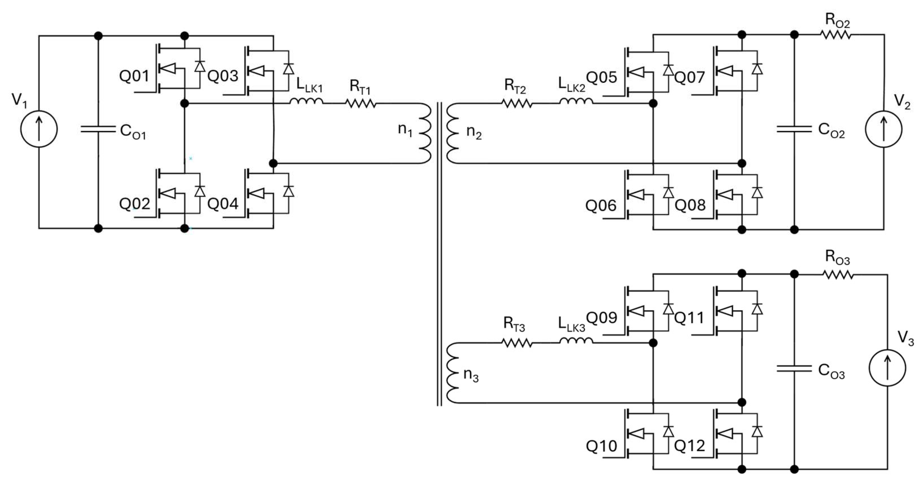
Equations (2) and (3) show that there is a coupling between the inputs: the output power on the secondary side is dependent on both phase shifts φ2 and φ3. The same principle applies to the tertiary side. While theoretically, the control loops could handle this and reach the steady state, the coupling will worsen the dynamics and can become problematic, especially in the presence of periodic oscillations. To obtain a decoupling algorithm, an accurate model of the TAB converter is required. The modelling of the TAB converter has been widely discussed, with models based on Fourier series approximation [19] with variations based on D-connection and Y-connection transformer equivalents, or reduced-order models [20], which replaces the dynamics of high-frequency currents with averaged values. For clarity, a reduced-order model of a TAB converter with three voltage sources representing the battery, the capacitor bank, and the DC-link is presented below (Figure 3).

2.1. Reduced-Order Model of the TAB Converter

The reduced-order model requires all parameters to be referenced to one side of the transformer. In this case, the primary (the DC-link) side is selected. All relevant parameters were transformed to the primary side (Equations (4)–(6)).
R k = n 1 n k 2 R k
L k = n 1 n k 2 L k
C k = n k n 1 2 C k
where: k = 1, 2, 3, n—transformer turn ratio.
The output voltages VC2 and VC3 are calculated using Kirchhoff’s Voltage Law (KVL). The time variant description “(t)” is discarded for clarity.
I 2 C O 2 d V C 2 d t 1 R O 2 V C 2 + 1 R O 2 V 2 = 0
I 3 C O 3 d V C 3 d t 1 R O 3 V C 3 + 1 R O 3 V 3 = 0
The averaged currents I 2 and I 3 are calculated based on the power equations (Equations (2) and (3)):
I 2 = φ 2 π φ 2 L l k 3 V 1 2 π 2 f s K L + π φ 2 φ 3 L l k 1 V C 3 2 π 2 f s K L + φ 3 ( π | φ 2 φ 3 | ) L l k 1 V C 3 2 π 2 f s K L
I 3 = φ 3 π φ 3 L l k 2 V 1 2 π 2 f s K L + π φ 3 φ 3 L l k 1 V C 2 2 π 2 f s K L + φ 2 ( π | φ 3 φ 2 | ) L l k 1 V C 2 2 π 2 f s K L
The component KL is used for clarity and is described as:
K L = L l k 1 L l k 2 + L l k 2 L l k 3 + L l k 1 L l k 3
Because the reduced-order model uses the averaged current values (Equations (9) and (10)) the dynamics of the transformer circuit are entirely discarded—including any parasitic components. The only exception is the transformer leakage inductance, which is lumped with external inductance as Llk1, Llk2, and Llk3. The dynamics of the reduced-order model are thus dependent only on the dynamics of its output filters, and the averaged currents provide information about the power transfer between ports.
Supplementing Equations (9) and (10) into Equations (7) and (8) yields a set of equations, which can be used to derive the state–space description of the system. The state vector is defined as [VC2,VC3]T, and the input vector is defined as [V2, V3, φ2, φ3]T. The primary voltage V1 is considered as constant. Then, the state and input matrices are as follows:
A =   1 R O 2 C O 2 0 0 1 R O 3 C O 3
B = 1 R O 2 C O 2 0 K 13 K 14 0 1 R O 3 C O 3 K 23 K 24
K 13 = π | φ 2 | L l k 3 V 1 2 π 2 f s K L + ( π | φ 2 φ 3 | ) L l k 1 V C 3 2 π 2 f s K L
K 14 = ( π | φ 2 φ 3 | ) L l k 1 V C 3 2 π 2 f s K L
K 23 = ( π | φ 3 φ 2 | ) L l k 1 V C 2 2 π 2 f s K L
K 24 = π | φ 3 | L l k 2 V 1 2 π 2 f s K L + ( π | φ 3 φ 3 | ) L l k 1 V C 2 2 π 2 f s K L
Due to the presence of coefficients K13, K14, K23, and K24 in the input matrix, the system is both non-linear and time-variant. The next step would be to linearize the model around an equilibrium point or a chosen point of operation; however, at this stage, the model is sufficient for simulation in MATLAB R2024b and Simulink if a dynamic state–space model is used (Figure 4, Figure A1 and Figure A2).

2.2. Decoupling of the Converter Inputs

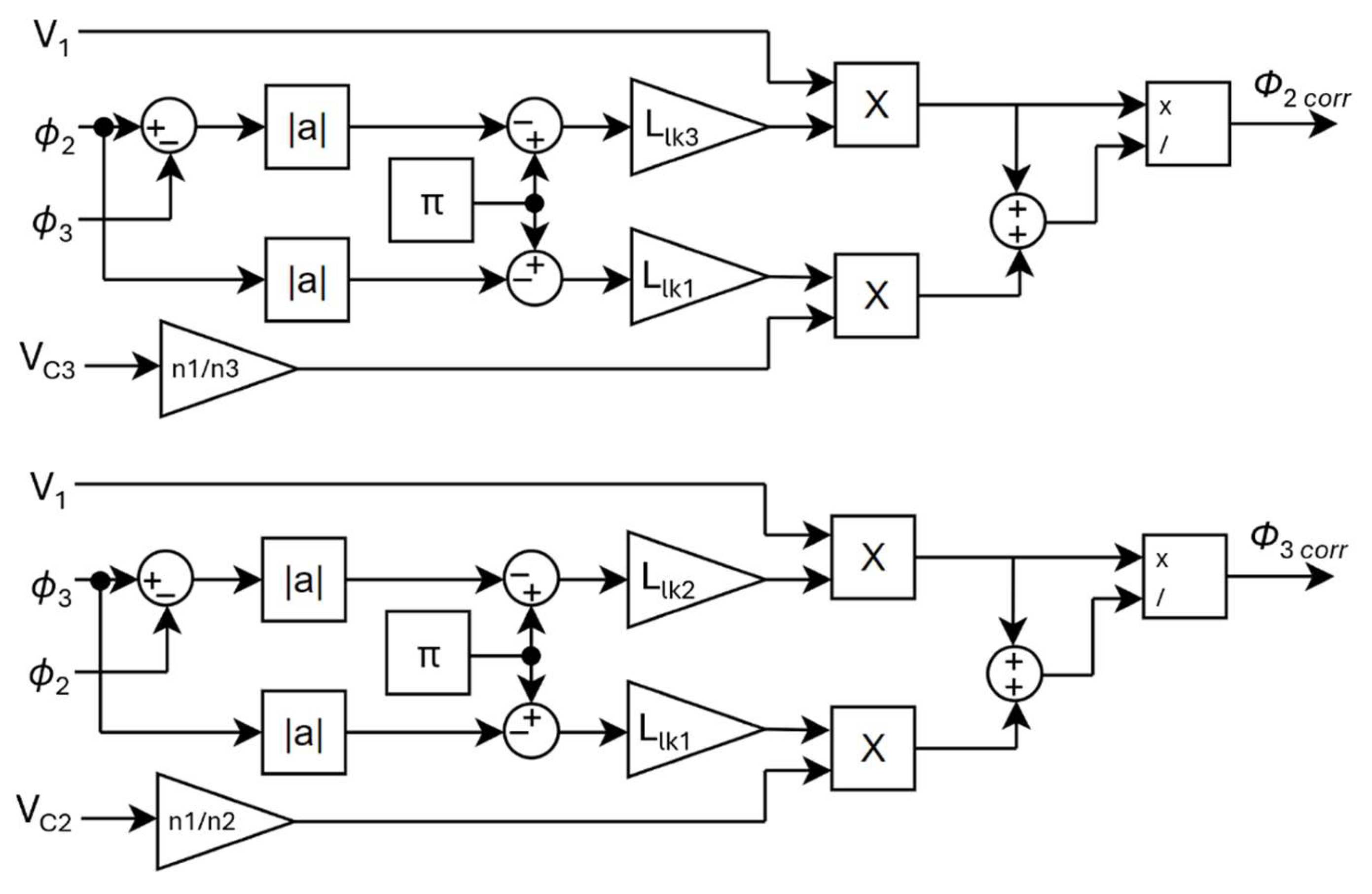
When analyzing the model, it can be seen that there are static elements—tied to output filter dynamics—and variable elements—derived from the averaged high-frequency currents. The system in its current form has coupled inputs, as seen in the input matrix (Equations (13)–(17)). Each state is dependent on three inputs: the port voltage, its own phase angle, and the other winding phase angle (i.e., VC2 tied to V2, φ2, and φ3). This coupling should be removed so that VC2 is only dependent on V2 and φ2, while VC3 is only dependent on V3 and φ3. This can be achieved by implementing a feedforward loop (Figure 5). In the latter part of the paper, whenever the coupling is discussed, cross-control refers to phase command to the opposite winding (i.e., φ2‘s influence on VC3) and direct-control refers to phase command controlling its own winding (i.e., φ2‘s influence on VC2).
The feedforward gains can be derived from the input matrix and are defined as:
G f f 1 = K 14 K 13
G f f 2 = K 23 K 24
After simplification, these terms become
G f f 1 = ( π | φ 2 φ 3 | ) L l k 1 V C 3 π φ 2 φ 3 L l k 1 V C 3 + ( π | φ 2 | ) L l k 3 V 1
G f f 2 = ( π | φ 3 φ 2 | ) L l k 1 V C 2 π φ 3 φ 2 L l k 1 V C 2 + ( π | φ 3 | ) L l k 2 V 1
These gains can be presented graphically (Figure 6).
These feedforward gains are dynamic and will require constant measurement of three port voltages and phase shift information to operate. In Equations (20) and (21), the leakage inductances are constants, the phase shifts are calculated by the controllers, and the voltages are the only quantities that are measured; as such, they are the most prone to inaccuracies and noise. In the discussed application, these measurements are performed with a switching frequency (fs = 20 kHz); they are also synchronized with the PWM waveforms and shifted to the center of the waveform to reduce the switching noise. To further improve the robustness of the measurements, they are performed in the differential mode. Another possible way of improving the measurement accuracy is to introduce averaging: by implementing multiple measurement points over one PWM period and then performing cycle-by-cycle averaging, or by averaging over multiple PWM periods, as the dynamics of the output filters and their respective voltages are much lower than that of the high-frequency circuit.

2.3. Design of the Control Loop

The main control loop aims to direct AC and DC components of the DC-link current to their respective destinations. To operate, it requires measurement of all three port currents, and with the decoupling algorithm, an additional three voltage measurements are necessary. The proposed control loop is presented in Figure 7.
The extraction of AC and DC components from the DC-link current is based on an exponential moving average (EMA) filter—which behaves like a low-pass filter and extracts the average value of the DC-link current—which corresponds to the DC component:
y t = k u t + 1 k y t 1
where: k—filtering coefficient, ut—input, yt—current sample output, and yt−1—previous sample output.
The EMA filter is built as a three-stage cascaded filter with more restrictive coefficients in each stage. This allows for preserving the dynamics while also improving the filtering. The AC component is obtained by subtracting the DC component from the DC-link current.
The extracted DC component is used as a reference for the PI controller, while the AC component is used as a reference for the PR controller. The controller parameters and the EMA filter parameters are presented in Table 1. The PR controller parameters were obtained by implementing the resonant controller in an infinite impulse response structure—those coefficients were calculated based on the target resonant frequency (fr = 100 Hz), controller execution frequency (fc = 20 kHz), and desired frequency band (Δf = 3 Hz). The EMA filter was implemented as a three-stage filter; its coefficients were adjusted during simulation to achieve the desired AC rejection. A three-stage filter with decreasing coefficients performed better than a single-stage filter with a minimal KEMA coefficient.

3. Simulation and Experimental Results

In order to verify the operation of the proposed algorithm, a laboratory bench was built along with a simulation model. The laboratory bench was set up to operate with lowered voltage (Figure 8). The simulation model reflects the values used on the laboratory bench. The key parameters of elements used to build the converter are presented in Table 2.
The control unit was based on a Texas Instruments C2000 series TMS320F28379D microcontroller, with voltage and current measurements based on the AMC1300B isolated operation amplifiers. The power circuit was based on three modular H-bridges, built on Infineon CoolSiC FF11MR12W1M1_B11 silicon carbide power modules.
The control application was developed in C language, to enable several modes of operation of the converter: open-loop mode, closed-loop mode with internal references, autonomous closed-loop mode, and an option to enable or disable the decoupling algorithm for all of those modes. The converter was managed via CAN 2.0b protocol, by another microcontroller connected directly to a PC. The measurement data was collected with an oscilloscope and processed in MATLAB. The full list of used measurement equipment is presented in Table 3.
While the experiment was performed in a system with lowered voltage, the discussed problem was strictly current-related, and the same behavior would be observed in a system with high voltage. Operation with high voltage would require higher-rated components, and due to increased switching losses, careful design of the cooling system would be required. In addition, an increase in voltage creates an increase in the electromagnetic interference, which will require input and output filters to ensure EMC compliance.

3.1. Open-Loop Testing

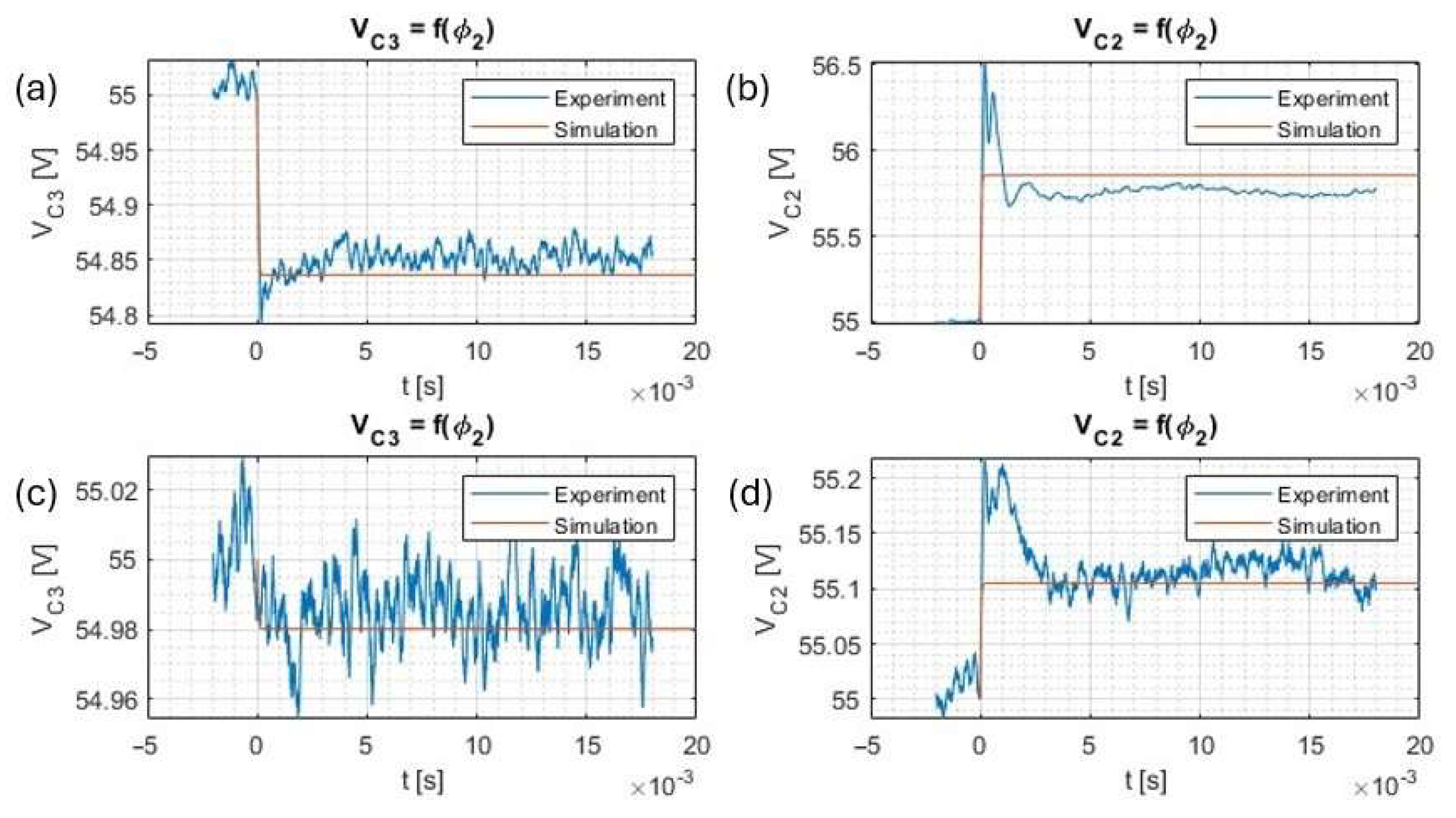
Open-loop testing was performed to confirm the accuracy of the developed reduced-order model. In order to test the converter, it was connected to three power supplies: on the primary side, ITECH IT6012C-800-40 (Power supply 1), and ITECH IT6015B-80-450 on the secondary (Power supply 2) and tertiary (Power supply 3) sides (Figure 9). The results are presented in Figure 10.
The open-loop test results show that the accuracy of the model is within 50 mV—with 40 mV of random noise. Dynamically, the simulation and the experiment follow the same rising slope; however, the experiment shows an overshoot, which is not present in the simulation. This overshoot is caused by the action of the power supply’s internal voltage controllers, which react more slowly than the converter. The tests were performed for small (0.02π) and large (0.2π) positive and negative phase shifts for both φ2 and φ3, and in all of those cases, the results retain their accuracy. The averaged value of the root mean squared error (RMSE) for those runs was 71 mV, if the overshoots are included in the analysis, and 21 mV if the overshoots are excluded. Similarly, the maximal RMSE if the overshoot was included was at 164 mV and 41 mV if the overshoot was excluded. The most problematic is the small step response to cross-control (i.e., VC3 reaction to φ2) as seen in Figure 10c, where the step response in the experiment is on a similar level to the random noise and as such is hard to evaluate.

3.2. Simulation of the Control Loop

After model verification, the next step was to test the design of the control loop. First, simulation testing was performed. There were several points to test:
  • Operation of the decoupling algorithm
  • Operation of the EMA filter
  • Operation of the PI/PR controllers
  • Operation of the standalone mode
  • Since the final control loops are current control loops, the tests evaluate the output current responses to the phase inputs.

3.2.1. Simulation of the Decoupling Algorithm

In order to verify the operation of the decoupling algorithm open-loop tests of the model were run: once without the decoupling and once more with the decoupling enabled.
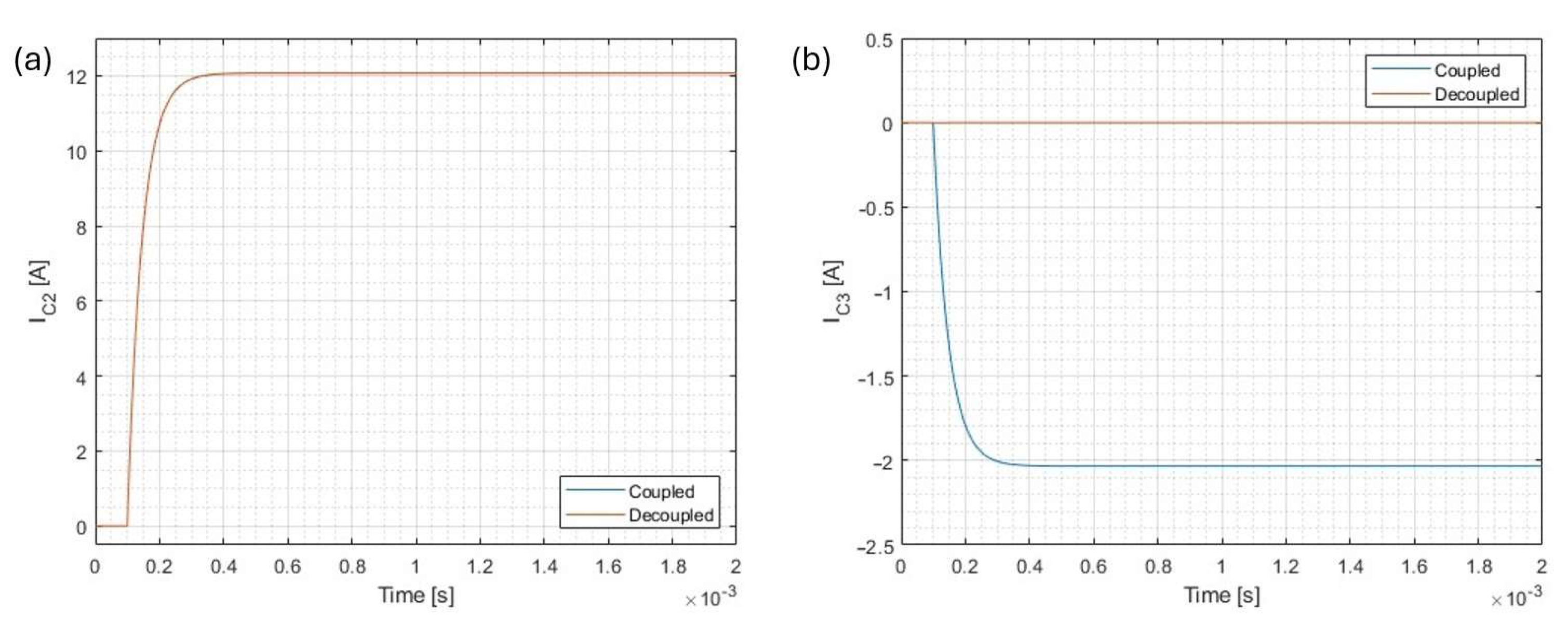
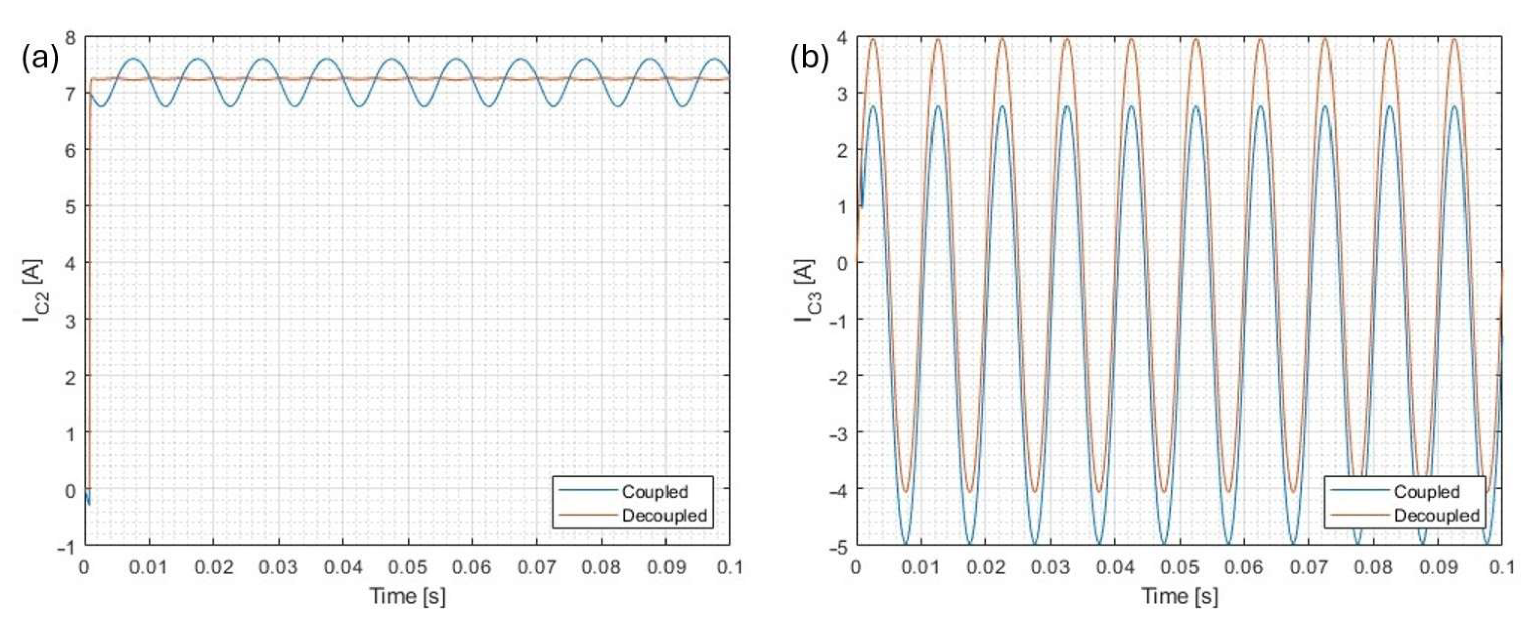
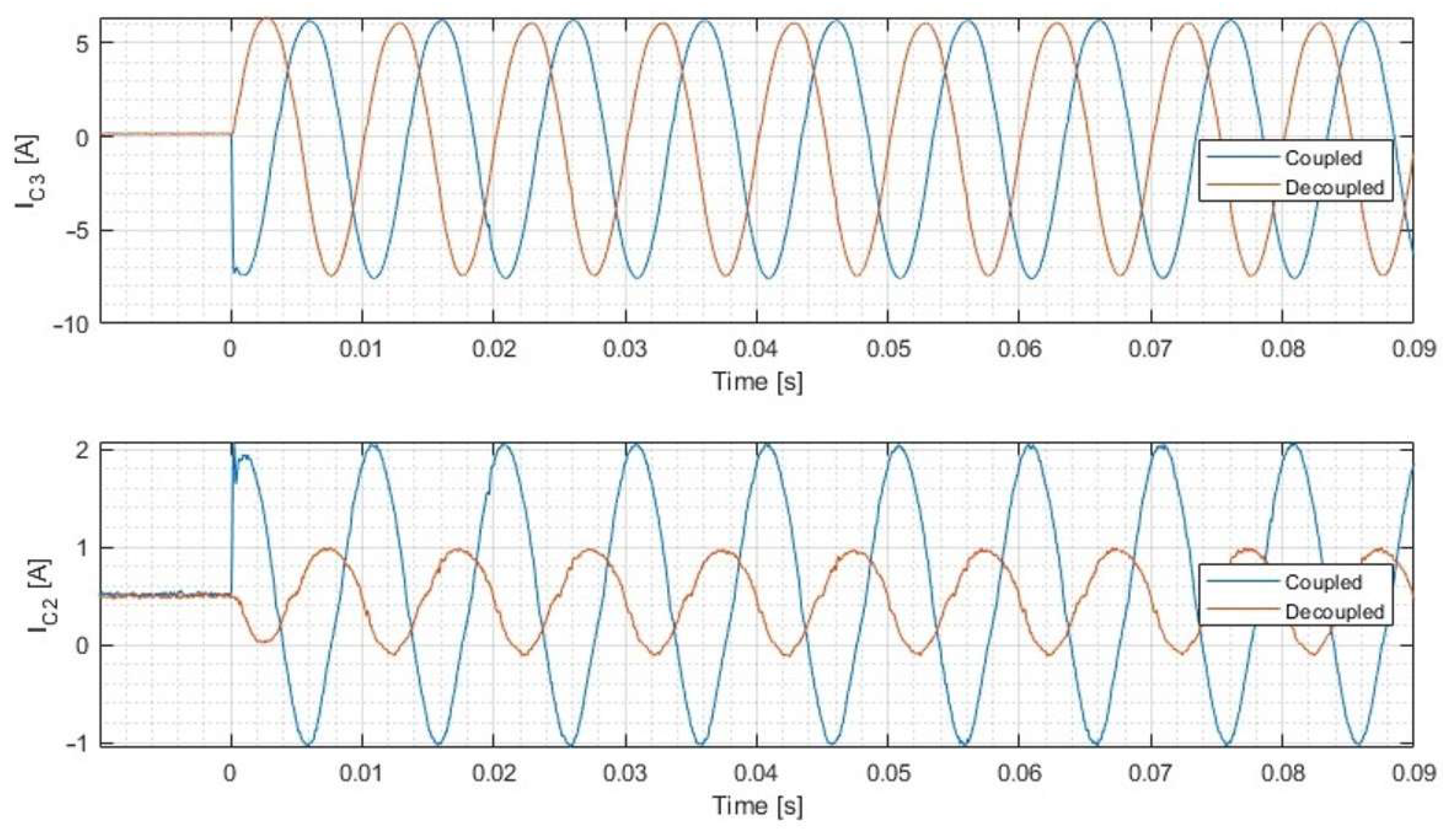
The response of the system to the direct control does not change, regardless of the application of the decoupling algorithm (Figure 11a). The response to cross-control is fully eliminated (Figure 11b). In Figure 11, whenever only the orange curve (the decoupled voltage) is visible, it covers the blue curve (the coupled voltage). Since the system aims to operate with a DC and 100 Hz AC component, a simulation was run with one of the bridges driven by a 100 Hz sinewave (Figure 12).
In the case of sinusoidal excitation, the benefit of the decoupling is more pronounced: the sinewave is removed from the IC2 current, and a DC offset is removed from the IC3 current (Figure 12). The proposed decoupling feedforward loop operates effectively for both constant and sinusoidal inputs.

3.2.2. Simulation of the Exponential Moving Average Filter

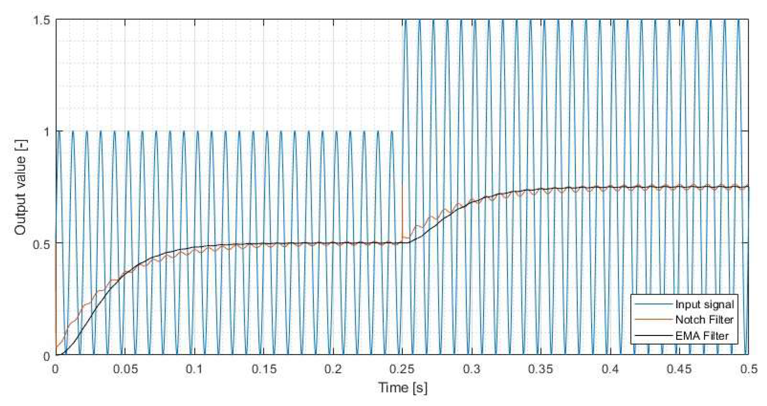
In order to evaluate the operation of the EMA filter, a simulation was set up to compare it with a solution based on the notch filter. The notch filter is tuned to remove the 100 Hz frequency from the DC-link current. Both the EMA filter and the notch filter responses follow a similar curve (Figure 13); however, the EMA filter removes the AC component more effectively. In the case of the notch filter, approximately 0.05 A of AC component remains in the signal. In addition, the notch filter reacts with a spike to any rapid change—this is due to the change being significantly faster than the execution frequency of the filter.

3.2.3. Simulation of the PI/PR Controllers

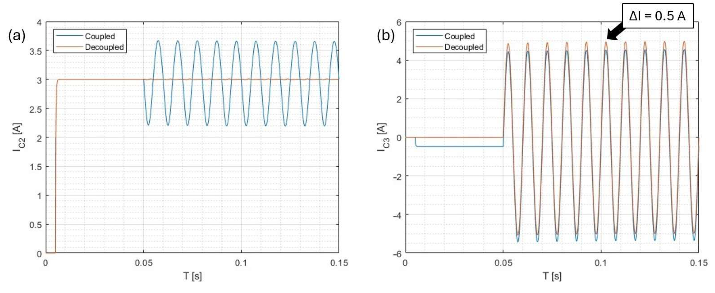
Evaluation of the PR/PI controller loops was performed with artificial reference signals. The results are presented in Figure 14.
In the simulation, both the PI and the PR controllers handle their respective references properly; however, the importance of the decoupling algorithm is clearly visible, as neither of the controllers is able to completely eliminate the error coming from the cross-control.

3.2.4. Simulation of the Standalone Mode

The standalone mode utilizes the same control loop, with the exception of the references for the controllers; those are generated by the EMA filter loop, splitting the DC-link current. The DC-link current behaves exactly the same as in the previous test; only the references are changed.
The results from the test show that the system takes approximately 0.08 s to reach a steady state for the battery current (Figure 15). The compensator current steadies marginally faster; however, it reacts to the DC value—this is due to the EMA filter processing the DC-link current. The PR controller in the compensator current loop reacts within 0.06 s to the sinewave step. Once more, the importance of the decoupling is highlighted—the battery current controller is unable to remove the pulsation from the coupling, and the compensator current control has a slight DC offset, which would lead to discharging (or charging) of the capacitor bank.

3.3. Experimental Verification of the Closed-Loop Operation

The first stage of the verification of the closed-loop operation was performed using the setup presented in Figure 9. The results were recorded using an oscilloscope and then processed in MATLAB.
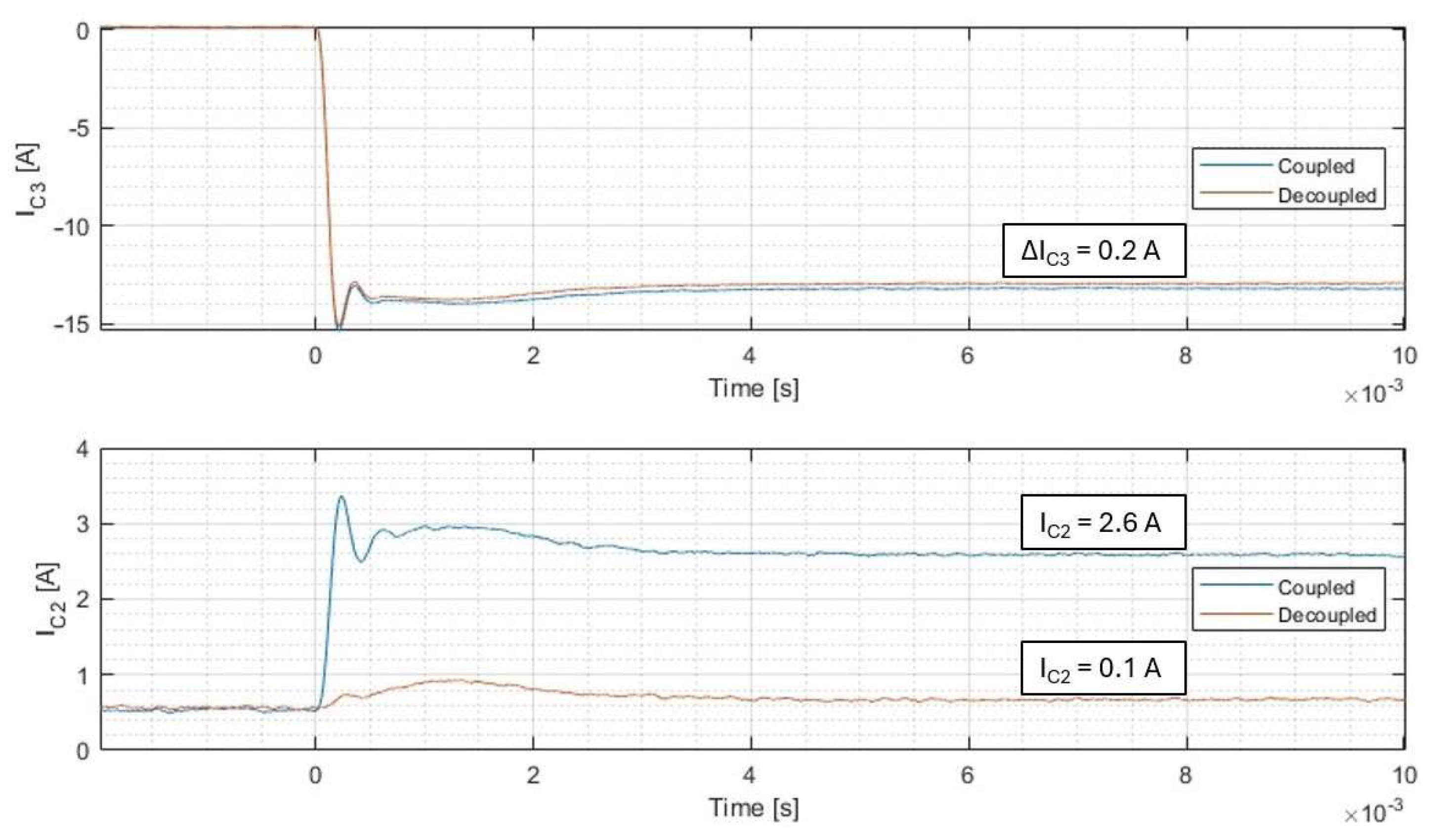
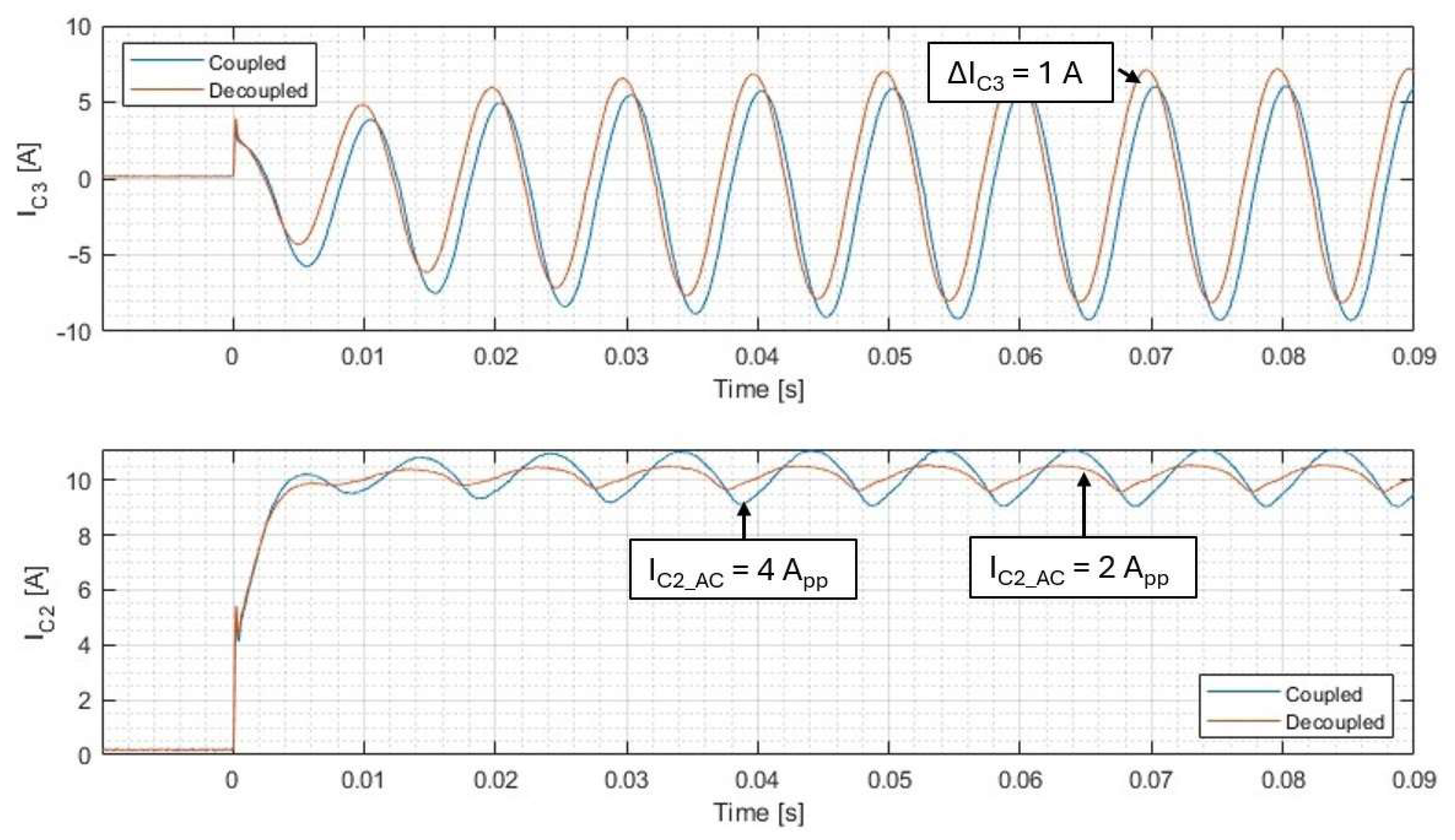
The open-loop step response achieved in the experimental setup (Figure 16) behaves in the same way as in the simulation (Figure 11). The response to direct control is barely influenced by the decoupling, whereas the response to the cross control is reduced: the output still responds during the dynamic state, but the response is several magnitudes lower. In the steady state, the coupling is reduced by 96%.
The response to the sinusoidal excitation (Figure 17) is much worse than the simulation (Figure 14)—only an approximately 67% reduction is achieved. Figure 17 shows phase shifts between coupled and decoupled responses—these are purely accidental, as both runs were separate.
The final run at this stage evaluated closed-loop operation with artificial references. The references were sent through the CAN protocol. The battery current reference was passed directly to the PI controller; the capacitor current reference was used as a magnitude for an internal sinewave generator. This generator produces a sinewave with a frequency of 100 Hz and a controllable magnitude.
The response in closed loop with the artificial reference shows that the decoupling removes DC offset from the compensator current and reduces the steady-state pulsation in the battery current (Figure 18). The reduction in this case comes from two sources: first, the PI controller, and then the decoupler.

3.4. Standalone Mode Operation

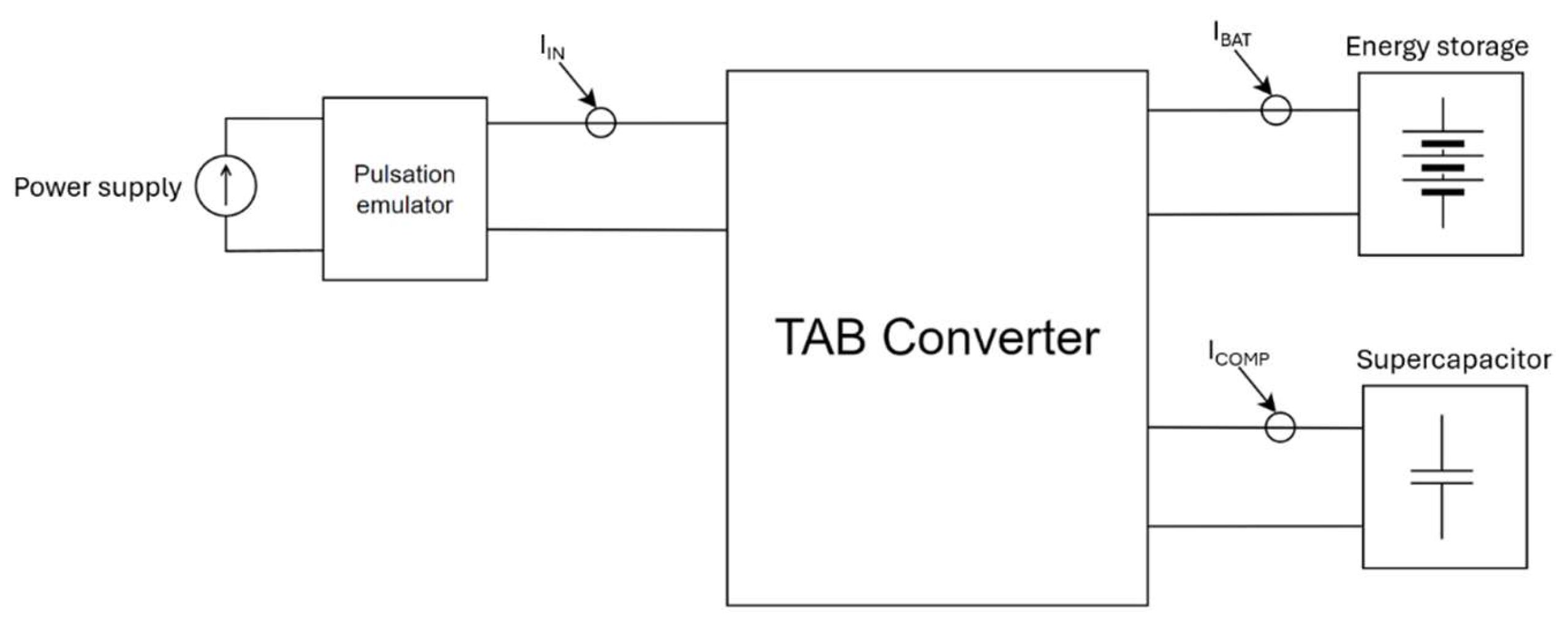
To test the standalone mode operation, the TAB converter was connected to a lithium-ion battery (Port 2), a supercapacitor (Port 3), and a DC-link emulator (Port 1). The buck-boost DC/DC converter was used to emulate the operation of a DC-link (Figure 19). The battery used for the experiment was a low-voltage battery BMZ ESS X, rated for 60 V of voltage and 10 kWh capacitance (during the experiment, the battery was partially charged and kept at 55 V). The capacitor used in the experiment was the LS Mtron supercapacitor, with a capacity of 93 F and a nominal voltage of 87 V. A DC and AC control loop was implemented on the emulator to generate variable currents in the DC-link (Figure 19). The emulator is controlled in controlled voltage mode, and as such, the resulting current is not directly controlled; however, this behavior still reflects the DC-link of an AC/DC converter.
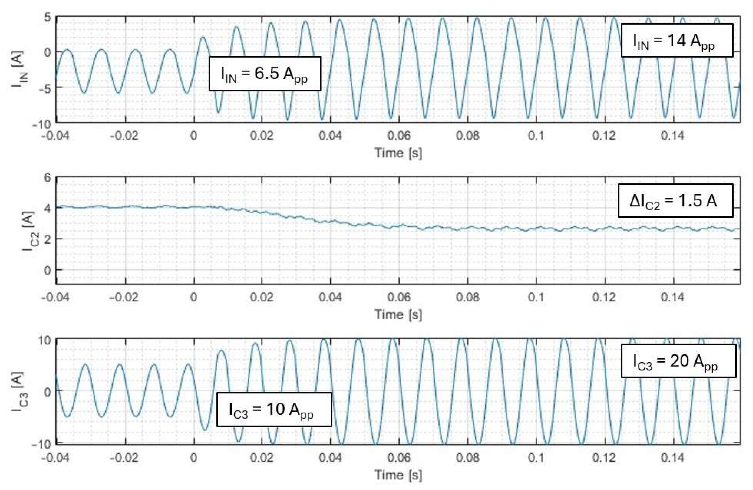
In the dynamic test, one or both components of the DC-link current were controlled, and the TAB converter reaction was observed. First, the response to an increase in the AC component was tested. The system reaches a steady state within 0.04 s. The reaction time is influenced only by the PR controller dynamics (Figure 20).
The response time is longer for a case in which there is an increase in the DC component; then, the EMA filter must respond, and since it is the component with the worst dynamics in the system, the response time is longer—at 0.08 s (Figure 21).
The key parameter of the proposed system is the ratio of the 100 Hz AC pulsation measured at the battery port compared to the 100 Hz AC pulsation measured at the DC-link. This reduction coefficient Kred is calculated as:
K r e d = 1 I B A T A C I I N A C n 1 n 2 100 %
where IBAT_AC—100 Hz component of the battery current and IIN_AC—AC component of the input current.
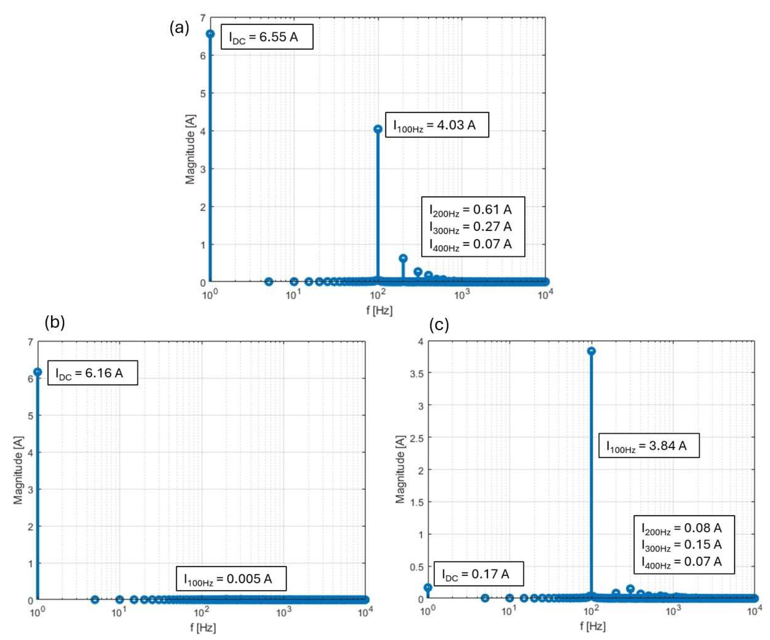
To extract the 100 Hz component magnitude, the steady-state currents of the TAB converter were measured for different AC and DC component values generated by the emulator and then they were processed in MATLAB by applying Fourier decomposition (Figure 22).
The FFT analysis was repeated for several cases. The lowest recorded reduction coefficient Kred was at 95.99%, while discharging the battery with a high AC component. The highest recorded Kred was at 99.88%, while charging the battery with a high AC component. On average, the Kred was at 98.3%.

4. Results Discussion

In this paper, we propose a DC-link current pulsation compensation system based on a triple-active bridge converter topology. This approach was tested through simulation, as well as in the experimental setup, which modeled the behavior of a DC-link of a four-wire AC/DC converter. A reduced-order model of the TAB converter with three voltage sources was developed to provide a foundation for a decoupling algorithm. A feedforward loop with dynamic gains was selected as a decoupling algorithm. This loop allowed for control of the power flow between the DC-link, the battery, and the capacitor independently and formed a basis for two separate control loops: one, based on a PI controller, to direct the DC current to/from the battery and another, based on a PR controller, which directs the AC current to the supercapacitor. The final element of the control loop was AC/DC component extraction, and an exponential moving average filter was selected to perform this role. The results show the importance of the decoupling algorithm in the system: the PI and PR controllers on their own are unable to eliminate the power flow resulting from the coupling of the converter. Simulation also shows that the decoupling can handle dynamic operation; in the experiment, the results were worse, and part of the oscillation still remained in the battery current. The compensation system takes approximately 0.08 s to reach a steady state—this time is longer when a large DC component change happens. If only the AC component of the DC-link current changes, then the delay is only the result of the PR controller, and the reaction time goes down to 0.04 s. Despite the long setting time of the battery current loop, the AC component is almost entirely eliminated from the battery port; an average reduction coefficient Kred of 98.3% was achieved in the experiment. Two factors contribute to this result: the outputs of the control loops and the decoupling algorithm.

5. Conclusions

In this paper, a DC-link current pulsation compensator based on a triple-active bridge topology is presented. This solution proved effective, achieving a 98.3% reduction in the AC component on the battery port. This result is comparable to other solutions in the authors’ previous work; a 97.3% reduction was achieved, with two parallel dual active bridges working in tandem and a sensorless compensation algorithm. Similar results can be achieved with non-isolated topologies. Fully sensored operation of the TAB converter (three current measurements and three voltage measurements), while more prone to measurement faults, also allows for independent operation: no information from the inverter is necessary, and it could be used as an expansion of already existing storage systems. With comparable compensation results, advantages and tradeoffs should be discussed. These are presented in (Table 4).
The use of the TAB-based solution trades efficiency and control complexity for higher power density—compared to a solution based on two parallel DAB converters. Both of these solutions are meant for operation with high voltage gain, required in applications in which a low-voltage energy storage is a necessity, due to local regulations.

Author Contributions

Conceptualization, K.F.; methodology, K.F.; software, K.F.; validation, K.F. and M.Z.; data curation, K.F.; writing—original draft preparation, K.F. and M.Z.; writing—review and editing, K.F. and M.Z. All authors have read and agreed to the published version of the manuscript.

Funding

This research received no external funding.

Conflicts of Interest

The authors declare no conflicts of interest.

Abbreviations

The following abbreviations are used in this manuscript:
EMAExponential moving average
PIProportional integral
PRProportional resonant
TABTriple-Active Bridge

Appendix A

Figure A1. Simulink model diagram for the reduced-order model simulation.
Electronics 14 03196 g0a1
Figure A2. Code snipped of the MATLAB function used to generate dynamic matrices A and B for the ROM model.
Electronics 14 03196 g0a2

References

  1. Vechiu, I.; Etxeberria, A.; Tabart, Q.; Lopez, R. Operational Limits of Four Wires Three Levels NPC Topology for Power Quality Improvement in Weak Grids. In Proceedings of the 2016 IEEE 16th International Conference on Environment and Electrical Engineering (EEEIC), Florence, Italy, 7–10 June 2016; pp. 1–5. [Google Scholar]
  2. Zieliński, D.; Stefańczak, B.; Jędrys, K. Phase-Independent Reactive Power Compensation Based on Four-Wire Power Converter in the Presence of Angular Asymmetry between Voltage Vectors. Energies 2022, 15, 497. [Google Scholar] [CrossRef]
  3. Ji, Y.; Wang, C.Y. Heating Strategies for Li-Ion Batteries Operated from Subzero Temperatures. Electrochim. Acta 2013, 107, 664–674. [Google Scholar] [CrossRef]
  4. Kacetl, T.; Kacetl, J.; Tashakor, N.; Goetz, S. A Simplified Model for the Battery Ageing Potential Under Highly Rippled Load. In Proceedings of the 2022 24th European Conference on Power Electronics and Applications (EPE’22 ECCE Europe), Hannover, Germany, 5–9 September 2022; pp. 1–10. [Google Scholar]
  5. Vermeer, W.; Stecca, M.; Mouli, G.R.C.; Bauer, P. A Critical Review on The Effects of Pulse Charging of Li-Ion Batteries. In Proceedings of the 2021 IEEE 19th International Power Electronics and Motion Control Conference (PEMC), Gliwice, Poland, 25–29 April 2021; pp. 217–224. [Google Scholar]
  6. Rąbkowski, J.; Król, K.; Zdanowski, M.; Skotnicki, M. GaN-Based Soft-Switched Active Power Buffer Operating at ZCS-Problems of Start-up and Shut-Down. Bull. Pol. Acad. Sci. Tech. Sci. 2020, 68, 785–792. [Google Scholar] [CrossRef]
  7. Komeda, S.; Ohnuma, Y. An Isolated Single-Phase AC-DC Converter Basedon a Dual Active Bridge Converter and an Active Energy Buffer Circuit. In Proceedings of the 2021 IEEE 30th International Symposium on Industrial Electronics (ISIE), Kyoto, Japan, 20–23 June 2021; pp. 1–6. [Google Scholar]
  8. Takeuchi, K.; Ohno, T.; Watanabe, H.; Nakata, Y.; Itoh, J.-I. Active Power Decoupling Method Based on Dual Active Bridge Converter without Additional Components. In Proceedings of the 2025 IEEE Applied Power Electronics Conference and Exposition (APEC), Atlanta, GA, USA, 16–20 March 2025; pp. 21–26. [Google Scholar]
  9. Wang, C.; Nehrir, M.H. Load Transient Mitigation for Stand-Alone Fuel Cell Power Generation Systems. IEEE Trans. Energy Convers. 2008, 22, 864–872. [Google Scholar] [CrossRef]
  10. Choi, M.-E.; Kim, S.-W.; Seo, S.-W. Energy Management Optimization in a Battery/Supercapacitor Hybrid Energy Storage System. IEEE Trans. Smart Grid 2012, 3, 463–472. [Google Scholar] [CrossRef]
  11. Fatyga, K.; Zieliński, D. Sensorless Current Pulsation Compensation in a Hybrid Energy Storage. Appl. Sci. 2023, 13, 2252. [Google Scholar] [CrossRef]
  12. Liu, C.; Li, B.; Zhang, Y.; Jiang, Q.; Liu, T. The LCC Type DC Grids Forming Method and Fault Ride-through Strategy Based on Fault Current Limiters. Int. J. Electr. Power Energy Syst. 2025, 170, 110843. [Google Scholar] [CrossRef]
  13. Cai, Y.; Li, J.; Gu, C.; Yang, J.; Guenter, S.; Buticchi, G.; Zhang, H. A Modular Modulation Decoupling Algorithm for Multiple Active Bridge Based Multiport EV Charger. IEEE J. Emerg. Sel. Top. Power Electron. 2024, 12, 3637–3649. [Google Scholar] [CrossRef]
  14. Costa, L.F.; Buticchi, G.; Liserre, M. Optimum Design of a Multiple-Active-Bridge DC–DC Converter for Smart Transformer. IEEE Trans. Power Electron. 2018, 33, 10112–10121. [Google Scholar] [CrossRef]
  15. Alam, M.D.; Mahinur Rahman, M.; Awal, M.A.; Husain, I.; Lukic, S. Pulsating Power Processing through Multi-Active Bridge for Electric Vehicle Charging Applications. In Proceedings of the 2024 IEEE Energy Conversion Congress and Exposition (ECCE), Phoenix, AZ, USA, 20–24 October 2024; pp. 2035–2041. [Google Scholar]
  16. Wasim, M.S.; Habib, S.; Amjad, M.; Bhatti, A.R.; Ahmed, E.M.; Qureshi, M.A. Battery-Ultracapacitor Hybrid Energy Storage System to Increase Battery Life Under Pulse Loads. IEEE Access 2022, 10, 62173–62182. [Google Scholar] [CrossRef]
  17. Lemian, D.; Bode, F. Battery-Supercapacitor Energy Storage Systems for Electrical Vehicles: A Review. Energies 2022, 15, 5683. [Google Scholar] [CrossRef]
  18. Vechiu, I.; Camblong, H.; Tapia, G.; Dakyo, B.; Curea, O. Control of Four Leg Inverter for Hybrid Power System Applications with Unbalanced Load. Energy Convers. Manag. 2007, 48, 2119–2128. [Google Scholar] [CrossRef]
  19. Okutani, S.; Huang, P.-Y.; Kado, Y. Generalized Average Model of Triple Active Bridge Converter. In Proceedings of the 2019 IEEE Energy Conversion Congress and Exposition (ECCE), Baltimore, MD, USA, 29 September–3 October 2019; pp. 5554–5560. [Google Scholar]
  20. Zou, S.; Lu, J.; Khaligh, A. Modelling and Control of a Triple-Active-Bridge Converter. IET Power Electron. 2020, 13, 961–969. [Google Scholar] [CrossRef]
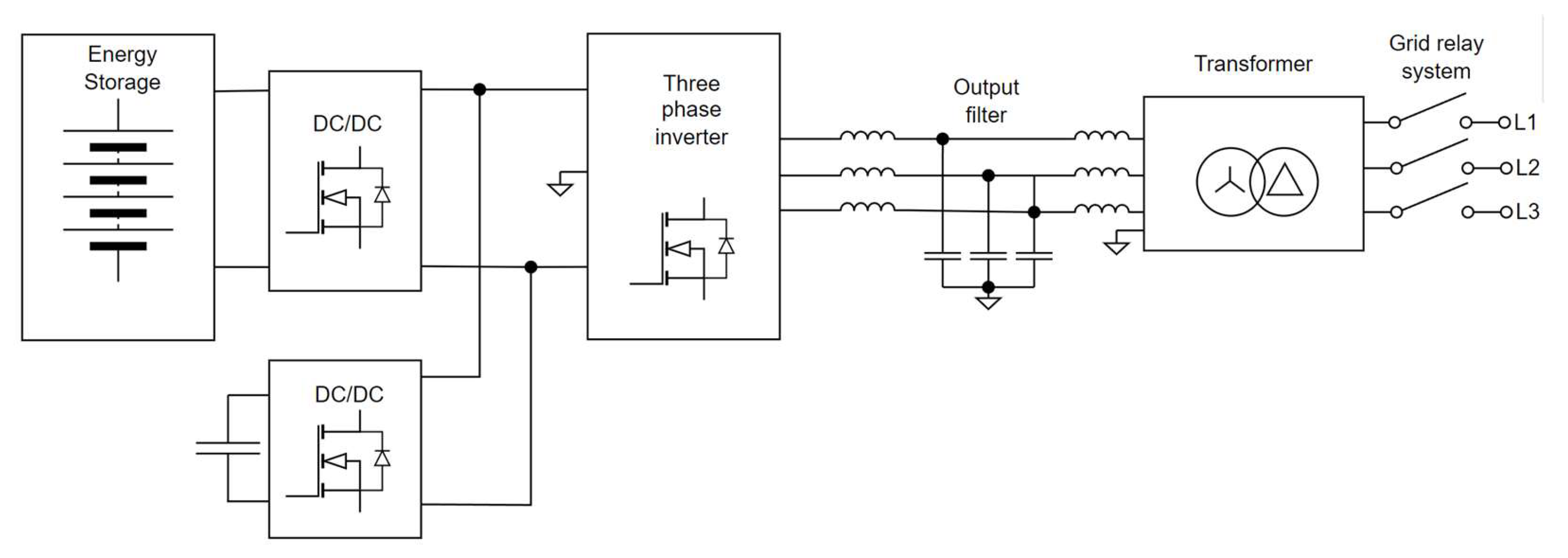
Figure 1. An energy storage system with a four-wire inverter and an additional DC/DC converter with a buffer.
Electronics 14 03196 g001
Figure 2. An energy storage system with TAB converter-based pulsation compensation.
Electronics 14 03196 g002
Figure 3. Diagram of the TAB converter with all key parameters.
Electronics 14 03196 g003
Figure 4. A block diagram of a simulation model with a dynamic state–space block.
Electronics 14 03196 g004
Figure 5. A feedforward loop for decoupling inputs.
Electronics 14 03196 g005
Figure 6. Graphical representation of the feedforward gains.
Electronics 14 03196 g006
Figure 7. AC pulsation compensation algorithm.
Electronics 14 03196 g007
Figure 8. Laboratory bench for testing of the pulsation compensation system.
Electronics 14 03196 g008
Figure 9. Laboratory bench diagram for open-loop testing.
Electronics 14 03196 g009
Figure 10. Step response of the TAB converter in an open loop: (a,c) φ2 = 0.02 and (b,d) φ2 = 0.2.
Electronics 14 03196 g010
Figure 11. Step response of the TAB converter with and without the decoupling algorithm: (a) direct-control response and (b) cross-control response.
Electronics 14 03196 g011
Figure 12. Step response of the TAB converter in an open loop with and without the decoupling algorithm: (a) battery port current IC2 and (b) capacitor bank current IC3.
Electronics 14 03196 g012
Figure 13. Step response comparison between the three-stage EMA filter and the notch filter.
Electronics 14 03196 g013
Figure 14. Closed-loop step response to constant IC2 = 3 A step at t = 0.005 s and IC3 = 5 × sin(2 × π × 100× t) A step at t = 0.05 s (a) secondary side (battery), (b) tertiary side (compensator).
Electronics 14 03196 g014
Figure 15. Closed-loop step response to constant IC2 = 3 A step at t = 0.005 s and IC3 = 5 × sin(2 × π × 100 × t) A step at t = 0.05 s with references from the EMA filter (a) secondary side (battery), (b) tertiary side (compensator).
Electronics 14 03196 g015
Figure 16. Open-loop step response of the TAB converter for a step φ3 = 0.2π.
Electronics 14 03196 g016
Figure 17. Open-loop step response of the TAB converter for a step of φ3 = 0.1 × sin(2 × π × 100 × t)π.
Electronics 14 03196 g017
Figure 18. Closed-loop response in the PI/PR controller mode for a simultaneous step of IC2 = 10 A, IC3 = 7 A, and f = 100 Hz.
Electronics 14 03196 g018
Figure 19. Diagram of the test bench used to evaluate operation in the standalone mode.
Electronics 14 03196 g019
Figure 20. A TAB converter’s response to an increase in the AC component: Step of VDCLink from 97.0 VDC + 10.0 VAC to 97.0 VDC + 14 VAC at time = 0 s.
Electronics 14 03196 g020
Figure 21. A TAB converter’s response to an increase in the DC component, without changes to the AC component: Step of VDCLink from 97.0 VDC + 14.0 VAC to 97 VDC + 14 VAC at time = 0 s.
Electronics 14 03196 g021
Figure 22. FFT analysis of the TAB converter currents: (a) primary side (DC-link), (b) secondary side (battery), and (c) tertiary side (supercapacitor).
Electronics 14 03196 g022
Table 1. Controller parameters.
ParameterValue
EMA Filter
First-stage coefficient KEMA10.007 [-]
Second-stage coefficient KEMA20.005 [-]
Third-stage coefficient KEMA30.002 [-]
PI Controller
Proportional Gain Kp1 [-]
Integral Gain KI100 [-]
High/Low Limits+/−0.25 [-]
PR Controller
Coefficient B00.0550 [-]
Coefficient B10 [-]
Coefficient B2−0.0550 [-]
Coefficient A01 [-]
Coefficient A11.9959 [-]
Coefficient A2−0.9969 [-]
Proportional gain Kg0.01 [-]
Controllers execution rate
Controllers frequency fc20 kHz
Table 2. Converter parameters.
ParameterUnitValue
Transformer parameters
Turn ratio, primary side n1-1.73
Turn ratio, secondary side n2-1.0
Turn ratio, tertiary side n3-1.0
Series transformer resistance RT1, RT2, RT30.02
Leakage inductance, primary side LLK1µH28.23
Leakage inductance, secondary side LLK2µH16.0
Leakage inductance, tertiary side LLK3µH17.96
Magnetizing inductance LMmH3.18
Port parameters
Input voltage, primary side, V1V92
Input voltage, secondary side, V2V55
Input voltage, tertiary side, V3V55
Output series resistance, secondary side RO20.1
Output series resistance, tertiary side RO30.1
Output capacitance, secondary side CO2µF460
Output capacitance, tertiary side CO3µF460
Other parameters
Switching frequency fskHz20
Total converter powerkW1.7
Table 3. Measurement equipment used in the laboratory tests.
ParameterUnit
OscilloscopeTektronix MSO5034B
Input port measurements I1, I2, I3Current probe: Tektronix A622
Transformer current measurementCurrent probe: MicSig CP2100A
Output voltage measurementsIsolated voltage probe: Pico TA057
Table 4. Comparison of TAB-based compensation vs. dual DAB-based compensation.
ParameterTABDual DAB
Number of power semiconductors1216
Transformers1, 3 windings2, 2 windings
ControlCentralized, single unitDecentralized, requires synchronization and robust communication
Control complexityComplex, requires decouplingModerate
Power densityHigherLower
EfficiencyLower, up to 96%, due to a more complex structureUp to 98%
Disclaimer/Publisher’s Note: The statements, opinions and data contained in all publications are solely those of the individual author(s) and contributor(s) and not of MDPI and/or the editor(s). MDPI and/or the editor(s) disclaim responsibility for any injury to people or property resulting from any ideas, methods, instructions or products referred to in the content.