Abstract
This paper presents a novel harmonic-selective clocking scheme that facilitates concurrent downconversion of spectrally distant radio frequency (RF) signals using a single low-frequency local oscillator (LO) in an N-path receiver architecture. The proposed scheme selectively generates LO harmonics aligned with multiple RF bands, enabling simultaneous downconversion without modification of the passive mixer topology. The receiver employs a 4-path passive mixer configuration to enhance harmonic selectivity and provide flexible frequency planning.The architecture is implemented on a printed circuit board (PCB) and validated through comprehensive simulation and experimental measurements under continuous wave and modulated signal conditions. Measured results demonstrate a sensitivity of and a conversion gain varying from to depending on the selected harmonic pair. The receiver’s performance is further corroborated by concurrent (dual band) reception of real-world signals, including a GPS signal centered at 1575 MHz and an LTE signal at 1179 MHz, both downconverted using a single 393 MHz LO. Signal fidelity is assessed via Normalized Mean Square Error (NMSE) and Error Vector Magnitude (EVM), confirming the proposed architecture’s effectiveness in maintaining high-quality signal reception under concurrent multiband operation. The results highlight the potential of harmonic-selective clocking to simplify multiband receiver design for wireless communication and global navigation satellite system (GNSS) applications.
1. Introduction
The continuous expansion of diverse frequency bands and wireless communication standards has significantly improved mobility and throughput in modern communication systems. However, this proliferation of standards and bands introduces challenges related to limited physical space and power consumption, complicating the integration of multiple individual receivers for simultaneous multiband reception.
N-path receivers have emerged as a compact and energy-efficient solution by leveraging digital signal processing techniques to replace bulky and power-hungry surface acoustic wave (SAW) filters. The elimination of SAW filters reduces receiver size and power consumption while enhancing reconfigurability. The fundamental principles, architectures, and performance characteristics of passive mixing-based receivers have been extensively studied [1,2,3,4]. These receivers demonstrate high linearity and offer flexible antenna matching across wide frequency ranges, achieving noise figures typically between 3 dB and 6 dB under optimal impedance matching conditions.
Significant progress has been made to optimize these mixers’ performance. For instance, ref. [5] presents a passive harmonic rejection mixer utilizing an 8-path topology that achieves third and fifth harmonic rejection with an operating bandwidth of 8–30 GHz and harmonic rejection exceeding 27 dB. Additionally, ref. [2] introduces an ultra-low-power (ULP) N-path mixer receiver achieving measured gains of approximately dB across ISM bands (430/860/915/960 MHz), a noise figure of dB, and an out-of-band IIP3 of dBm.
A notable advancement in passive mixers is the development of concurrent (dual band) reception techniques, which reduce circuit complexity, chip area, and power consumption while preserving reconfigurability and linearity. One approach involves sweeping the local oscillator (LO) frequency to sequentially downconvert multiple RF inputs, as demonstrated in [6], where the LO frequency is dynamically tuned across three values to downconvert signals at 0.836 GHz, 1.88 GHz, and 1.455 GHz.
Alternative methods exploit LO harmonics for simultaneous concurrent reception. Several recent works have explored the use of clock harmonics for frequency downconversion, each offering unique trade-offs in terms of harmonic selection, clocking architecture, reconfigurability, and application focus. These designs demonstrate the potential of harmonic-based local oscillator (LO) techniques in achieving compact and energy-efficient RF front-end architectures, particularly for multi-band systems.
For instance, in [7] employs a fixed 3-phase clocking scheme using only the 3rd harmonic. While the design maintains a low-power profile for narrowband IEEE 802.11 applications, it lacks the reconfigurability needed for dynamic or concurrent operation. In contrast, ref. [8] introduces a highly reconfigurable 32-phase LO architecture that leverages higher-order harmonics such as the 5th, 9th, 14th, and 15th for GNSS and IoT signals. Although this architecture offers excellent flexibility and digital harmonic rejection calibration, it introduces significant complexity and power overhead in LO generation.
Other dual-band architectures such as that in [9] employ a series configuration of two mixers and transformerbased matching networks to downconvert two RF bands. Each path requires its own quadrature N-path passive mixer, baseband amplifier, and dedicated LO generation, leading to increased circuit duplication. Similarly, the design in [10] proposes a dual-mode reconfigurable Hartley front-end for mmWave applications using off-chip LOs and frequency triplers, supporting both the 24.6–28 GHz and 55.6–60 GHz bands.
While these approaches demonstrate the feasibility of harmonic-based dual-band receivers, they either require duplicated hardware paths, involve complex clock generation schemes, or lack the flexibility needed for dynamic spectrum access. This motivates the need for a more compact, reconfigurable solution that enables simultaneous dual-band operation with reduced architectural complexity. This paper is organized as follows: Section 2 introduces the principle of harmonic-selective clocking. Section 3 presents a theoretical analysis of key RF receiver performance metrics. Section 4 discusses the receiver’s behavior in real-time application scenarios. Section 5 presents a comparison between the proposed architecture and conventional dual-band receiver designs, highlighting key differences in complexity, flexibility, and performance. Finally, Section 6 concludes the paper and summarizes the main findings. In addition, it discusses the key novelties of the proposed harmonic selective clocking technique and receiver architecture.
2. Harmonic Selective Clocks
Our proposed clock, as depicted in Figure 1, consists of two pulses with variable widths, and . The clock pattern repeats every , whereas the time duration of these two pulses together for every path is equal to . depends on the number of paths used in the passive receiver; for 4 paths, , while for 8 paths, . Precisely, is computed as the time period divided by the number of paths N. The amplitude of the clock harmonics is contingent upon , which represents the ratio of the duration of within , while is related to the duration of within . To ensure non-overlapping pulses, the positioning of the pulses in each path is altered; they can be delayed, flipped, or both flipped and delayed. Although the magnitude of the harmonics for each path within the receiver remains the same, there are discrepancies in their phases.
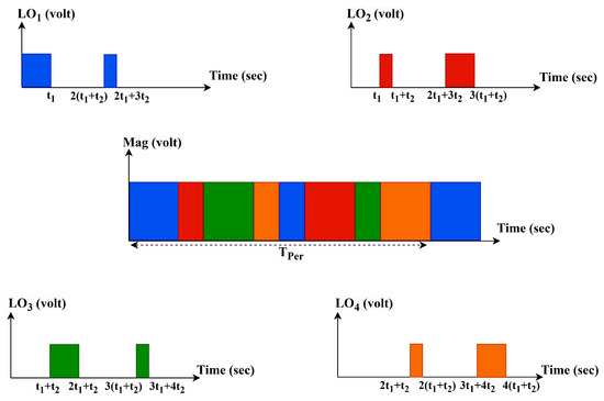
Figure 1.
Proposed harmonic selective clock.
To maintain time-domain isolation between signal paths in the multi-phase N-path receiver, the clock waveforms are carefully synthesized such that each path is activated by a pulse of equal amplitude but with a different phase. As shown in Figure 1, the clock signals through are designed with non-overlapping active intervals ensuring that, at any given time, only one switch is turned on while the others remain in the off state.
Each clock waveform consists of narrow pulses that control the switching transistors in the N-path structure. The blue trace () initiates the sequence at µs, while the red trace () represents a phase-inverted version of , with its rising edge aligned to the falling edge of the original clock. The green waveform () introduces a fixed time delay relative to , and the orange waveform () mirrors this delay across the inverted axis. Together, these four waveforms create a quadrature-like phase spacing, dividing the clock period into four distinct non-overlapping time slots, effectively distributing the switching activity over the full clock cycle.
The proposed clock scheme for a specific can be modeled and expressed using a Fourier series as:
where the Fourier coefficients are given by:
With the constants , , and defined as:
Figure 2 shows the relationship between the clock harmonics magnitudes and . The first four harmonics are illustrated, as this scheme suppresses the rest of the harmonics. The clock harmonics magnitude depends on ; for instance, , the third and fourth harmonics have equal magnitudes, while the first and second harmonics can be easily filtered out. This feature is useful in various wireless systems, such as GNSS reception, particularly for capturing GPS signals L1 (1575.42 MHz) and L5 (1176.45 MHz) using a low-frequency LO of 393 MHz. When , the second and fourth harmonics have high magnitudes, and the first and third harmonics are suppressed. For , the second and third harmonics are significant, the fourth harmonic is suppressed, and the first harmonic can be filtered out. Table 1 displays the varying clock harmonics magnitudes for different values.
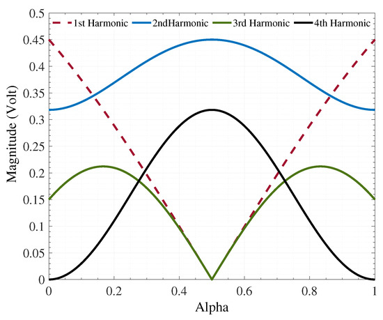
Figure 2.
Harmonic selective clock harmonics magnitude for different .

Table 1.
Clock harmonics magnitudes across different values.
To better highlight the significance of this scheme, Figure 3 compares the harmonic selective clock scheme for , , and with a single uniform clock for a 25% duty cycle. Since a phase-locked loop (PLL) is not integrated on the PCB, an external signal source (Agilent 81130 pulse generator, Keysight Technologies, Santa Rosa, CA, USA) is used to provide the local oscillator (LO) input. Both the single-clock and the proposed multi-phase clocking schemes employ the first four harmonics of a 150 MHz LO signal. The black dashed lines indicate the single uniform clock, while the orange dashed lines illustrate the harmonic selective clock scheme. As shown in Figure 3a, the proposed clock and the single clock with a duty cycle of 25% exhibit identical magnitudes for the first three harmonics. However, a key advantage of the proposed scheme is the significant suppression of the fourth harmonic, which is reduced by approximately 25 dB compared to the single-clock scheme. This harmonic shaping results in a spectrum where the first harmonic can be effectively filtered out, leaving the second and third harmonics with relatively high magnitudes. This selective enhancement of non-harmonically related clock components enables efficient simultaneous downconversion of two distinct frequency bands without relying on integer harmonic relationships, thereby demonstrating a major advantage of the proposed clocking technique. Similarly, in Figure 3b, which targets the downconversion of two frequencies that are not harmonically related, the proposed scheme allows the third and fourth harmonics of the clock to maintain comparable magnitudes. This facilitates effective downconversion using both components. Meanwhile, the first and second harmonics are substantially attenuated and can be easily filtered out. In contrast, the single clock scheme exhibits a significantly weaker fourth harmonic, making it unsuitable for dual band downconversion in this scenario.
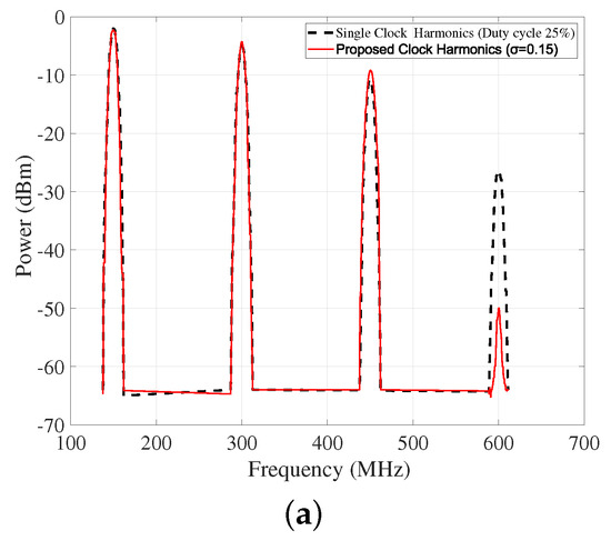
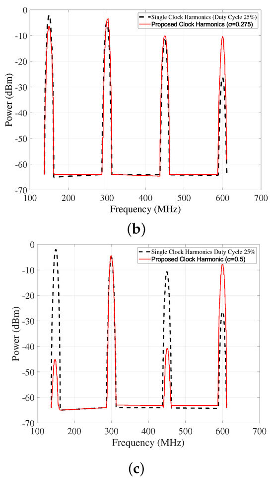
Figure 3.
Harmonics of proposed clock vs. uniform clock: (a) , (b) , (c) .
In the case of harmonically related frequencies, shown in Figure 3c, the proposed clock emphasizes the second and fourth harmonics while almost completely suppressing the first and third. This targeted spectral shaping allows the downconversion of two harmonically related input signals with minimal interference from undesired clock components.
Overall, the proposed clocking technique offers greater spectral control compared to the single pulse scheme. It enables the selective enhancement and suppression of clock harmonics to accommodate both harmonically and non-harmonically related downconversion scenarios, thereby improving flexibility and performance in multi-band receiver architectures.
3. Proposed Receiver Analysis
3.1. Input Impedance
The proposed receiver, shown in Figure 4, operates as a current-driven passive mixer with an input signal , which is the superposition of two concurrent signals, and . Each input signal has a frequency that is a few megahertz higher than the local oscillator (LO) frequency.
where n and m denote the harmonic orders of the local oscillator (LO) used to downconvert each signal.
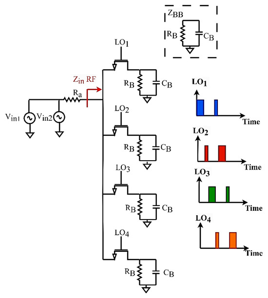
Figure 4.
4-path receiver with non-uniform clocks.
The total input current is:
The input signal passes through four MOSFET switches, which are assumed to be ideal in this analysis except for having a nonzero ON resistance denoted by . These four switches are driven by the harmonic-selective clock (non-overlapping) and terminated with four identical baseband loads, , each composed of the parallel combination of a baseband resistance and a baseband capacitance modeled as:
These terminations produce the four baseband outputs: , , , and . For simplicity of analysis, we will consider only one of the four paths corresponding to the first two harmonics as shown in Figure 5. In Figure 5a, the current is applied to the switch network and is multiplied by the harmonic-selective clock waveform , resulting in a baseband current at the output. The switching action enables frequency translation by mixing the signal down to the desired baseband frequency.
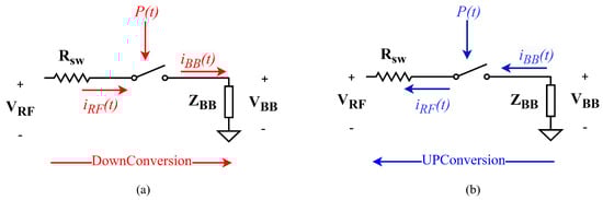
Figure 5.
(a) Downconversion of current to baseband current via harmonic-selective switching using the clock waveform ; (b) upconversion of baseband current back to the domain due to the bidirectional nature of the passive switches. The figure highlights the dual behavior of the switching network and the importance of harmonic selectivity in preserving receiver linearity and spectral isolation.
In contrast, Figure 5b illustrates the reverse process that occurs due to the bidirectional nature of the passive switches. Here, the previously generated baseband current is effectively upconverted back to the domain by multiplication with the same clock waveform .
In downconversion, the resulting baseband current after passing through one path is:
where the clock waveform for the first two harmonics is:
After filtering the far way bands,
The baseband voltage , generated by the flow of baseband current into the corresponding baseband impedance, is defined as:
To evaluate the input impedance of the proposed receiver, the side voltage of the mixer switches is examined during the upconversion operation. In this mode, the passive mixer leverages its bidirectional signal translation property, allowing baseband signals to be upconverted to the domain. Due to the non-overlapping nature of the harmonic-selective clocking scheme, only one switch is active at any given time. As a result, the instantaneous voltage is the sum of the corresponding baseband voltage and the voltage drop across the conducting switch. This drop is modeled as , where represents the switch ON resistance. Accordingly, the voltage during upconversion is given by:
Applying Fourier transform to and assuming that and have equal amplitudes, the resulting frequency-domain representation of the voltage can be expressed as:
denotes the product of the Fourier series coefficients defined in Equation (2), representing both the downconversion from to baseband and the subsequent upconversion from baseband back to . This phenomenon arises due to the bidirectional behavior of the switches in the system, which leads to signal reradiation. Consequently, the input impedance of the proposed receiver can be expressed as the sum of contributions from the four mixer paths, assuming . By dividing the voltage by the input current , the input impedance is given by:
For in-band signals, the above series can be truncated at the fourth order. Consequently, the input impedance of the receiver can be expressed as a linear combination of the baseband circuit impedances evaluated at frequencies , , , , and , respectively:
Figure 6 shows the input impedance for , , and with varying values of , computed using Equation (13). For consistency with prior work [3], the switch ON resistance was set to in both the theoretical analysis and ADS harmonic balance simulations. The simulations assume ideal switches, an antenna impedance of , and a baseband capacitance of pF.
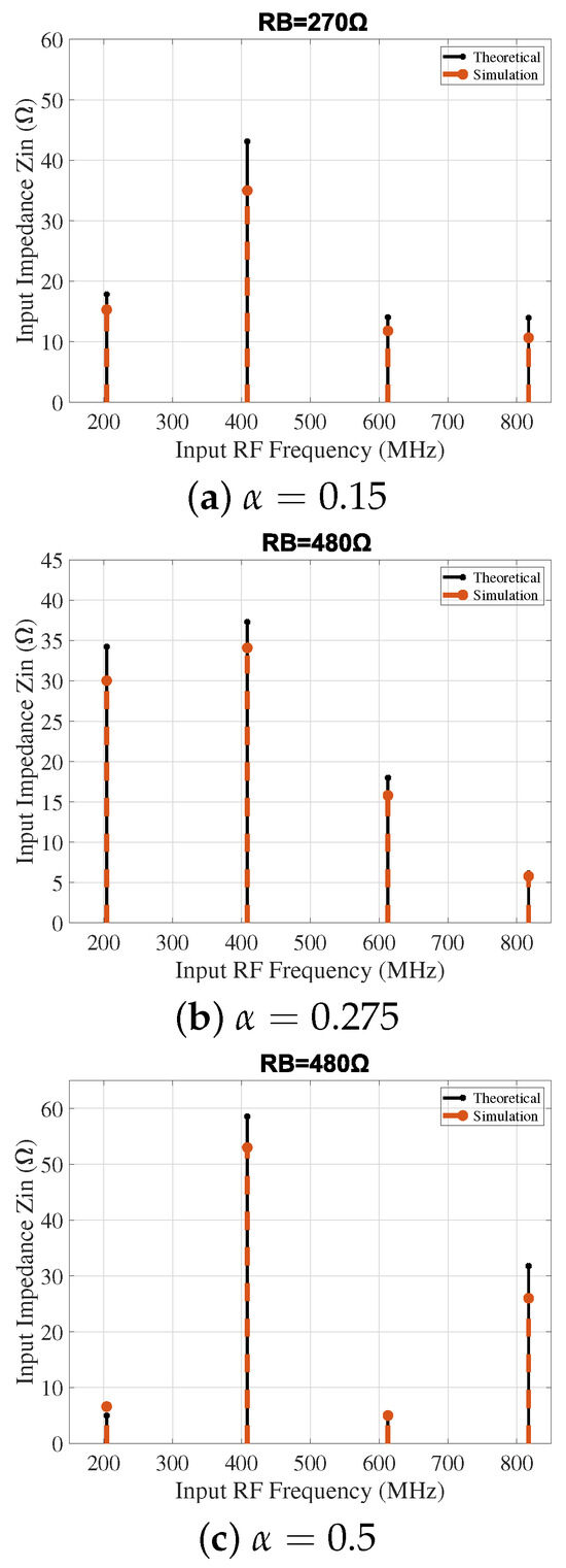
Figure 6.
Proposed receiver input impedance for different values.
3.2. Selectivity and Conversion Gain
Another critical performance metric for the proposed receiver is the conversion gain, which quantifies the efficiency of the frequency translation process. It is defined as the ratio of the output baseband voltage to the input radio frequency () voltage :
The out-of-band (OOB) rejection of the proposed receiver is another important performance metric. Similar to the conventional N-path receiver architecture [3]. This rejection characteristic is primarily influenced by the switch resistance , which determines the selectivity of the mixer network. The outband rejection can be expressed as:
To determine the bandwidth of the proposed receiver, we adopt the Linear Time-Varying (LTV) model introduced in [3]. This modeling approach provides valuable insight into the behavior of passive mixers, particularly emphasizing the bidirectional current flow facilitated by the switch operation. Due to the time-varying nature of the switches, current can flow between the and ports, enabling partial energy reflection back toward the antenna interface [3].
This re-radiated current arises from the voltage mismatch between the mixer’s baseband filter capacitors and the antenna input, effectively introducing an antenna-dependent shunt resistance, denoted as , in parallel with the baseband resistance [3]. The value of is not constant; it varies as a function of the duty cycle of the LO switching waveform, and can be expressed as:
where is the switch resistance, and represents the antenna resistance. This shunt resistance directly impacts the frequency response of the receiver, and thus plays a critical role in determining its overall bandwidth.
The cutoff frequency is:
The parameters in Table 2 confirm close agreement between simulated and measured results across different duty cycles and harmonic configurations. Measured conversion gain remains within 0.5 dB from simulation results, while bandwidth varies by no more than 1–3 MHz.
Table 2.
Simulation and measured results.
Lower-order harmonics with smaller duty cycles result in higher gain and narrower bandwidth, while higher-order harmonics combined with larger duty cycles widen the bandwidth at the expense of gain. This trade-off enables a tunable design space, allowing the receiver to adapt efficiently to different frequency bands and system requirements through simple adjustments to the clock waveform.
3.3. Sensitivity
Receiver sensitivity defines the minimum input signal power that can be reliably detected and processed. It is a fundamental performance metric in communication systems, as it determines the weakest signal level at which the receiver maintains acceptable operation. High sensitivity enables the detection of weaker signals, which is critical for long-range communication and operation in noisy environments.
To evaluate receiver sensitivity, the input power was swept from to , and the corresponding conversion gain was observed. The receiver maintained its reported conversion gain down to an input level of . Even at , it exhibited only a drop in gain compared to , demonstrating gradual degradation and robust performance under low-signal conditions.
Noise figure (NF) serves as an additional metric that complements the sensitivity analysis by quantifying the degradation in signal-to-noise ratio (SNR) introduced by the receiver. In conventional passive receiver architectures, the noise figure is typically equal to the insertion loss (conversion gain). In our proposed design the noise figure ranges from to , depending on the selected value of the parameter .
4. Modulated Signal Testing and Performance Evaluation
To evaluate the performance of the proposed architecture, it is essential to test it in real-time applications using modulated signals such as LTE, 5G, and GPS. The evaluation includes confirming downconversion with acceptable conversion gain, as discussed in Section 3.2. Additionally, it assesses the agreement between transmitted and received I/Q components, along with metrics such as normalized mean square error (NMSE) and error vector magnitude (EVM). Table 3 summarizes the parameters used in the modulated signal tests.
Table 3.
Signal configuration summary for concurrent reception.
Simulation tests were conducted using the ADS simulator with Envelope simulation, configured to include 32 harmonics for both the frequencies and the local oscillator (LO), ensuring better accuracy and results. The practical setup for the modulated signal tests is shown in Figure 7. Concurrent modulated signals were generated using MATLAB® 2024a and uploaded to the National Instruments PXIe-1075 transceiver, Austin, TX, USA. Harmonic clocks for the proposed architecture were generated using an Agilent 81130A pulse generator configured for two pulse widths. These clocks were then combined and phase-shifted using signal combiners.
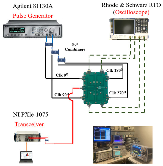
Figure 7.
Practical setup for the modulated signal test.
4.1. IF Downconversion Validation
To validate the downconversion performance of the proposed receiver, a series of measurements were conducted as summarized in Table 3. Test 1 involved the simultaneous application of an LTE signal with a carrier frequency of 818.5 MHz, a bandwidth of 1.4 MHz, and 64-QAM modulation, alongside a 5G signal centered at 618 MHz with a 5 MHz bandwidth and the same 64-QAM modulation scheme. The local oscillator was configured at 204.3 MHz, with the harmonic-selective clock employing a scaling factor . As shown in Figure 8, the normalized input spectra are centered at their respective frequencies , while the corresponding downconverted outputs appear at their intermediate frequencies . Both signals achieved a measured conversion gain of approximately dB, consistent with theoretical predictions, which further demonstrates the receiver’s capability to effectively downconvert multiple modulated signals across distinct frequency bands using a single LO source.
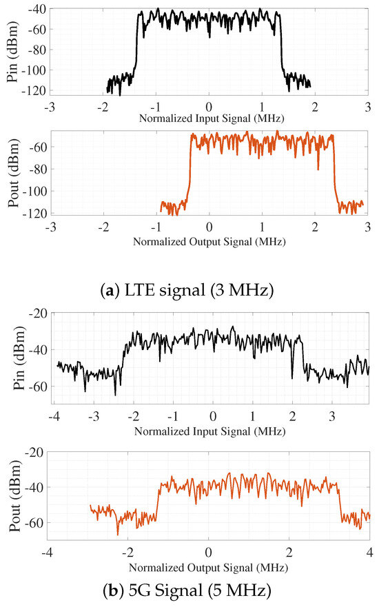
Figure 8.
Simulated input and output modulated signals of the proposed concurrent passive receiver for (a) LTE signal (3 MHz) and (b) 5G signal (5 MHz).
In Test 2, the two modulated signals used in the previous test were practically tested. Both the LTE and 5G were simultaneously applied at an input power level of dBm as presented in Figure 9. The LTE signal was downconverted to an intermediate frequency (IF) of 1.5 MHz, while the 5G signal was translated to 5 MHz. The local oscillator frequency was set to 204.3 MHz with . As shown in Figure 9, both signals achieved a measured conversion gain of approximately dB. These results closely match theoretical predictions and further validate the effectiveness and reconfigurability of the proposed receiver.
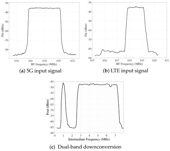
Figure 9.
Practical measurement for input signals and corresponding multiband downconverted output: (a) 5G signal centered at 618 MHz with a 5 MHz bandwidth and 64-QAM modulation, (b) LTE signal centered at 818.5 MHz with a 1.4 MHz bandwidth and 64-QAM modulation, and (c) the resulting downconverted output demonstrating simultaneous dual-band reception.
Test 3 presents a distinct frequency configuration that further demonstrates the capability of the proposed receiver to simultaneously downconvert a GPS L1 signal with a carrier frequency of 1575.45 MHz and a bandwidth of 2 Hz, alongside an LTE signal centered at 1179 MHz with a 3 MHz bandwidth. Both signals employ 64-QAM modulation. The local oscillator was configured at 393 MHz, and the harmonic-selective clock utilized an value of 0.275. As illustrated in Figure 10, the normalized input signals are centered at their respective frequencies (), while the corresponding downconverted outputs appear at their intermediate frequencies (). Both signals achieved a measured conversion gain of approximately dB, which is consistent with theoretical expectations and further demonstrates the receiver’s effectiveness in concurrently processing widely spaced signals using a single LO source.
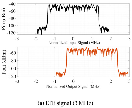
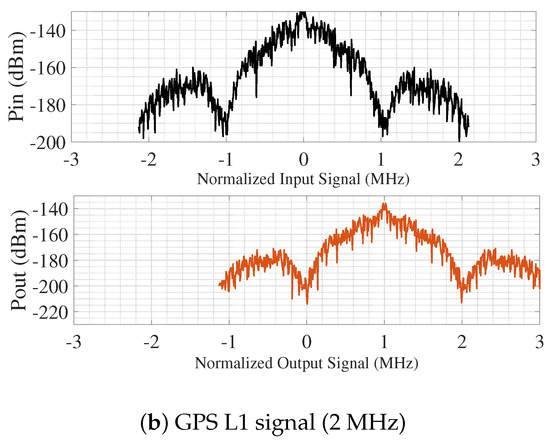
Figure 10.
Simulated input and output modulated signals of the proposed concurrent passive receiver for (a) LTE signal (3 MHz) and (b) GPS L1 signal (2 MHz).
4.2. Normalized Mean Square Error
The previous tests highlight the receiver’s ability to simultaneously downconvert two concurrent bands to their respective bands, achieving accurate downconversion with the expected conversion gain for both signals. Another important test to validate the receiver’s performance is the evaluation of the Normalized Mean Square Error (NMSE). Normalized Mean Square Error (NMSE) is a widely adopted metric that measures how accurately a receiver can reconstruct or estimate an input signal by quantifying the error between the received and reference signals, normalized to the power of the original signal. This normalization enables consistent, scale-independent comparisons across varying signal strengths and modulation types. NMSE is typically expressed in decibels (dB), where lower (more negative) values indicate better performance. For example, an NMSE of suggests that the error power is 1000 times lower than the signal power, reflecting excellent estimation accuracy. In contrast, higher (less negative or even positive) NMSE values imply greater distortion or noise influence, indicating degraded receiver performance. NMSE is particularly important in multi-band and complex modulation environments where precise signal recovery is critical for minimizing bit errors, maintaining synchronization, and ensuring robust demodulation. As such, NMSE serves as a key performance indicator for evaluating the effectiveness of receiver architectures under realistic operating conditions.
The normalized mean square error (NMSE) was assessed through simulation tests to further evaluate the receiver’s performance.
For the LTE signal described in Test 2, the I and Q components of both the input and output signals are shown in Figure 11. The NMSE for the I component was calculated to be −13.30 dB, while the NMSE for the Q component was −17 dB. Similarly, for the GPS signal in Test 2, the I and Q components of the input and output signals are shown in Figure 12. The NMSE for the I component was −16.02 dB, and for the Q component, it was −16.02 dB.
where is the ideal signal and is the received signal at sample n.
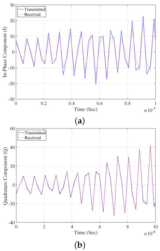
Figure 11.
Transmitted and received in-phase (I) (a) and quadrature (Q) (b) signals of an LTE signal having 3 MHz bandwidth at 1179 MHz signal carrier frequency.
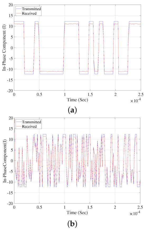
Figure 12.
Transmitted and received in-phase (I) (a) and quadrature (Q) (b) signals of a GPS signal having 2 MHz bandwidth at 1575 MHz signal carrier frequency.
4.3. Error Vector Magnitude
Error Vector Magnitude (EVM) is a fundamental metric for evaluating the quality of digitally modulated signals, particularly in systems employing in-phase (I) and quadrature (Q) components. It quantifies the deviation between the received and ideal signal points in the complex constellation plane by computing the root mean square (RMS) magnitude of the error vectors [11]. These error vectors capture the combined effects of amplitude and phase distortions accumulated throughout the signal path [11].
EVM provides a comprehensive measure of overall signal integrity by capturing the effects of key impairments encountered in wireless communication systems.
EVM is often expressed as a percentage, Lower EVM percentages indicate higher signal fidelity, while higher values suggest increased distortion due to factors such as noise, nonlinearities, phase noise, or IQ imbalance.
The Error Vector Magnitude (EVM) is calculated using the following equation:
where is the ideal signal and is the received signal at symbol k.
Figure 13 illustrates the variation of EVM over time for both GPS and LTE signals. While EVM is not a standard metric typically used to evaluate GPS performance, it can be computed based on its modulation scheme BPSK in this case making it a useful indicator of signal quality. The GPS signal exhibits EVM values ranging from 1.88% to 8.3%, with a mean around 4%. Lower EVM values indicate better signal fidelity, while higher values suggest the presence of distortion or degradation. The observed variation in EVM for GPS signals can be attributed to their inherently weak power levels typically below the thermal noise floor which makes them more susceptible to noise, interference, and multipath effects, especially in dynamic or obstructed environments where signal attenuation and reflection are more prominent.
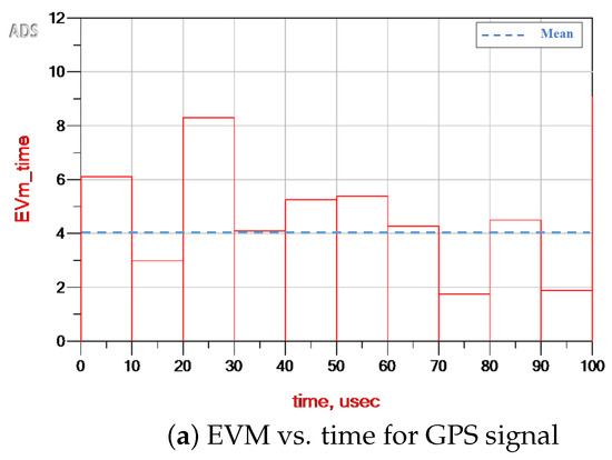
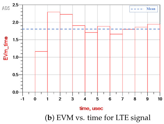
Figure 13.
EVM vs. time plots for (a) GPS signal and (b) LTE signal.
In contrast, the LTE signal demonstrated significantly lower and more stable EVM values, varying between 1.16% and 2.294% with a mean around 1.8%. These values fall well within the acceptable limits defined by communication standards such as 3GPP [12], which typically require EVM to remain below 8% for 64-QAM modulation. This confirms that the LTE signal was consistently received with high quality. For comparison, similar work reported in [9] achieved EVM values of 8.8% and 7.1% for a modulated dual-carrier 1.28 MS/s 16-QAM signal.
The EVM results presented in this paper provide valuable insight into the receiver’s performance under varying signal conditions. Although both signals were successfully demodulated, the higher and more fluctuating EVM observed in the GPS signal indicates a greater sensitivity to noise and interference.
5. Discussion
This work introduces a novel harmonic-selective clock generation technique integrated within a concurrent, reconfigurable passive mixer receiver. The proposed architecture enables simultaneous downconversion of two bands, regardless of whether they are harmonically related (e.g., ) or non-harmonically related (e.g., , ), using a single receiver path. A central innovation lies in the ability to dynamically control the amplitude of specific clock harmonics, providing flexible selection of mixing components for dual-band operation without requiring duplication or modification of the front-end. Additionally, the local oscillator (LO) operates at a frequency up to four times lower than the input, simplifying LO generation.
The receiver employs a compact 4-phase clocking scheme that selectively utilizes the 2nd, 3rd, and 4th clock harmonics in programmable pairs. This design achieves high reconfigurability with minimal circuit complexity, making it well-suited for multi-band applications such as LTE, 5G, and GNSS, where both harmonic agility and bandwidth flexibility are crucial. The clock waveforms are carefully engineered to ensure equal magnitudes and distinct phase shifts, enabling non-overlapping mixing intervals and preventing interference between signal paths.
When compared to conventional dual-band receiver architectures, the proposed solution offers notable advantages. Superheterodyne receivers, although known for their excellent selectivity, require multiple frequency translation stages including several mixers and filters which contribute to higher power consumption, increased design complexity, and a larger footprint. Moreover, their inherent architecture is not optimized for concurrent dual-band reception due to the need for multiple tunable LO paths and chains.
Direct conversion receivers eliminate intermediate frequency stages and reduce complexity, but often require separate I/Q paths for each band. This results in duplicated LO and circuitry, increased power draw, and potential layout inefficiencies. Furthermore, these architectures are prone to DC offsets and I/Q imbalance, which present additional challenges for dual-band implementations.
Subsampling-based architectures can downconvert signals directly to baseband using undersampled clocks. However, they are highly sensitive to jitter, noise folding, and spurious components. Concurrent dual-band operation using subsampling typically requires separate sampling paths or stringent LO control, limiting their practicality in low-power or compact designs.
In contrast, the proposed architecture leverages harmonic-selective clocks within a single N-path passive mixer structure to enable concurrent dual-band reception without duplicating front end hardware. This approach combines the inherent reconfigurability, compactness, and low complexity of the N-path architecture with the high linearity characteristics of MOSFET switches, while maintaining excellent spectral agility and signal integrity. These attributes make it particularly attractive for modern multi-band systems requiring flexibility and integration.
6. Conclusions
This paper presented a novel dual-band receiver architecture based on a harmonic-selective, reconfigurable passive mixer design. By integrating a 4-path passive mixer with a flexible clocking scheme that selectively activates higher-order harmonics, the proposed system enables simultaneous downconversion of two widely spaced signals using a single, low-frequency local oscillator (LO). This approach eliminates the need for duplicated receiver chains and simplifies LO generation, achieving both hardware efficiency and spectral agility within a compact footprint.
A key contribution of this work is the ability to dynamically control the harmonic content of the LO signal, allowing the receiver to target arbitrary frequency pairs including non-harmonically related bands, without altering the analog front-end. Furthermore, the linear time-varying (LTV) input impedance model was extended by leveraging the bidirectional nature of passive mixer switches, offering deeper insight into impedance transparency and signal re-radiation phenomena.
The proposed architecture was validated through harmonic balance simulations and a fabricated proof-of-concept PCB prototype. Experimental results confirmed strong out-of-band rejection, tunable conversion gain from dB to dB, and a minimum detectable input power of dBm. Signal fidelity was verified using normalized mean square error (NMSE) and error vector magnitude (EVM), with NMSE ranging from dB to dB and EVM values meeting the requirements of modern wireless standards.
Overall, the demonstrated performance highlights the proposed receiver’s potential for future multi-band wireless communication and sensing applications that demand reconfigurability, energy efficiency, and compact integration.
Author Contributions
D.I.: Methodology, Validation, Formal analysis and Original draft written; M.H.: Supervision; N.E.-S.: Supervision; F.G.: Supervision, Writing—review and editing. All authors have read and agreed to the published version of the manuscript.
Funding
Funding from the Natural Sciences and Engineering Research Council of Canada (NSERC), project number RT 73 2800.
Data Availability Statement
Dataset available on request from the authors.
Conflicts of Interest
The authors declare no conflict of interest.
References
- Atalla, E.S.; Zhang, F.; Balsara, P.T.; Bellaouar, A.; Ba, S.-N.; Kiasaleh, K. Time-domain analysis of passive mixer impedance: A switched-capacitor approach. IEEE Trans. Circuits Syst. Regul. Pap. 2017, 64, 347–359. [Google Scholar] [CrossRef]
- Lei, L.; Han, F.; Liu, Z.; Qi, Q.; Wang, X.; Wang, W. A 320 µW multi-band receiver with N-path switched-capacitor networks. Electronics 2022, 11, 4111. [Google Scholar] [CrossRef]
- Kammari, R.; Pasupureddi, V.S. Breaking the Trade-off Between Input Impedance and Mixer Paths in Sub-Harmonic N-Path Mixer-First RF Front-end. In Proceedings of the 2025 IEEE International Symposium on Circuits and Systems (ISCAS), London, UK, 25–28 May 2025; pp. 1–5. [Google Scholar] [CrossRef]
- Liu, Y.; Fang, Y.; Gao, H. A 60 GHz down-conversion passive mixer in 65 nm CMOS technology. In Proceedings of the 2021 IEEE MTT-S International Wireless Symposium (IWS), Nanjing, China, 23–26 May 2021; pp. 1–3. [Google Scholar] [CrossRef]
- Ahmed, A.; Rebeiz, G.M. A 8–30 GHz passive harmonic rejection mixer with 8 GHz instantaneous IF bandwidth in 45RFSOI. In Proceedings of the 2022 IEEE Radio Frequency Integrated Circuits Symposium (RFIC), Denver, CO, USA, 19–21 June 2022; pp. 19–22. [Google Scholar] [CrossRef]
- Qi, G.; Mak, P.I.; Martins, R.P. High-performance SAW-less TDD/FDD RF front-ends. In Analog and Mixed-Signal Circuits in Nanoscale CMOS; Springer: Berlin/Heidelberg, Germany, 2023; Chapter 1; pp. 3–25. [Google Scholar]
- Im, J.; Kim, H.-S.; Wentzloff, D.D. A 217 µW −82 dBm IEEE 802.11 Wi-Fi LP-WUR using a 3rd-harmonic passive mixer. In Proceedings of the 2018 IEEE Radio Frequency Integrated Circuits Symposium (RFIC), Philadelphia, PA, USA, 10–12 June 2018; pp. 172–175. [Google Scholar] [CrossRef]
- Wu, H.; Murphy, D.; Darabi, H. A harmonic-selective multi-band wireless receiver with digital harmonic rejection calibration. IEEE J. Solid-State Circuits 2019, 54, 796–807. [Google Scholar] [CrossRef]
- Ye, J.C.; Antón, A.H.; Sadeghi, S.; Huang, R.H.; Molnar, A.C. A simultaneous dual-carrier transformer-coupled passive mixer-first receiver front-end supporting blocker suppression. IEEE J. Solid-State Circuits 2025, 60, 1541–1553. [Google Scholar] [CrossRef]
- Yu, Y.; Ouyang, Z.; Huo, X.; Zhao, C.; Liu, H.; Wu, Y. A 28-/60-GHz dual-band receiver front-end with sideband-selection technique in 65-nm CMOS. IEEE Trans. Circuits Syst. I Regul. Pap. 2024, 71, 4550–4559. [Google Scholar] [CrossRef]
- Manurkar, P.; Silva, C.P.; Kast, J.; Horansky, R.D.; Williams, D.F.; Remley, K.A. Reference measurements of error vector magnitude. In Proceedings of the 2022 IEEE/MTT-S International Microwave Symposium—IMS 2022, Denver, CO, USA, 19–24 June 2022; pp. 1026–1029. [Google Scholar] [CrossRef]
- 3GPP. Evolved Universal Terrestrial Radio Access (E-UTRA) and Evolved Universal Terrestrial Radio Access Network (E-UTRAN); Overall description; Stage 2. In 3GPP TS 36.300; Version 17.0.0; 3GPP: Valbonne, France, 2019. [Google Scholar]
Disclaimer/Publisher’s Note: The statements, opinions and data contained in all publications are solely those of the individual author(s) and contributor(s) and not of MDPI and/or the editor(s). MDPI and/or the editor(s) disclaim responsibility for any injury to people or property resulting from any ideas, methods, instructions or products referred to in the content. |
© 2025 by the authors. Licensee MDPI, Basel, Switzerland. This article is an open access article distributed under the terms and conditions of the Creative Commons Attribution (CC BY) license (https://creativecommons.org/licenses/by/4.0/).