Abstract
The non-uniform thermal distribution in the active neutral-point clamped (ANPC) topology causes significant thermal gradients during high-power operation, restricting its use in large-capacity power conversion systems like variable-speed pumped storage. This study introduces a novel hybrid fundamental frequency modulation strategy. Through a dynamic allocation mechanism based on a reference signal, this strategy alternates inner and outer power switches at the fundamental frequency, ensuring balanced switching frequency across devices. Consequently, it effectively mitigates the inherent loss imbalance in conventional ANPC topologies. Quantitative analysis using a power device loss model shows that, compared to conventional carrier phase-shift modulation, the proposed method reduces total system losses by 39.98% and improves the loss-balancing index by 18.27% over inner-switch fundamental frequency modulation. A multidimensional validation framework, including an MW-level hardware platform, numerical simulations, and test data, was established. The results confirm the proposed strategy’s effectiveness in improving power device thermal balance.
1. Introduction
As the global energy transition accelerates, the share of renewable energy sources like wind and solar power in the grid continues to grow, profoundly affecting its stability [1,2]. Energy storage, a key regulatory resource, is essential for maintaining grid stability. Among energy storage technologies, pumped storage dominates due to its large capacity, long lifespan, and low cost [3,4,5]. However, conventional pumped storage systems exhibit slow dynamic responses and limited regulation accuracy, which constrain their effectiveness in providing fast frequency regulation, accurate real-time power balancing, and flexible ancillary services required by modern power grids. As a result, variable-speed pumped storage, with rapid response, adaptability to water head variations, and broad regulation range, has become a key trend in pumped storage evolution [6].
The high power capacity and cost constraints of full-power converters make large-scale implementation of variable-speed pumped storage units above 300 MW challenging. Consequently, AC excitation variable-frequency technology remains the preferred choice for large-capacity variable-speed pumped storage projects [7]. By adjusting the rotor winding current’s frequency and phase, this technology enables wide-range, continuous speed regulation, ensuring fast dynamic response and strong grid support. Additionally, as the converter processes only slip power, its capacity requirement is significantly lowered. As the core of an AC excitation system, the converter’s performance directly impacts unit efficiency and overall system reliability. Converter topologies fall into two main categories: indirect AC-DC-AC and direct AC-AC conversion. For high-power, high-voltage applications, cascaded H-bridge (CHB), and modular multilevel converters (MMC) are widely used for their voltage-stacking capability [8,9]. Among these, multilevel topologies are the dominant choice for high-power converters, as their stepped output reduces switching stress, enhances waveform quality, and minimizes filter size. In multilevel topologies, the traditional neutral-point clamped (NPC) inverter generates a three-level output using clamping diodes. However, it has inherent drawbacks, including uneven power loss distribution and neutral-point voltage fluctuations [10,11,12], which restrict output power. To mitigate these issues, the active neutral-point clamped (ANPC) topology replaces some clamping diodes with active switches, allowing for flexible state control. This method optimizes loss distribution, enhances voltage balancing, and boosts system efficiency, ultimately increasing power capacity [13,14,15]. However, the additional switches in ANPC topology increase control complexity. Moreover, uneven loss distribution and related thermal management challenges hinder its large-scale application.
A suitable pulse-width modulation (PWM) strategy provides a more practical solution than topology optimization for mitigating uneven temperature rise in ANPC three-level inverters. Without hardware modifications, a well-designed PWM strategy can balance power loss and adapt to varying load conditions [16,17,18,19], ensuring the long-term stability of high-capacity converters. The PWM strategy directly controls power device states and indirectly affects their loss characteristics. To address switching loss imbalances, various modulation strategies have been proposed. To address switching loss imbalances, various modulation strategies have been proposed. Ma et al. [17] introduced modulation waves that enable internal and external switches to achieve distinct sequences by selecting an appropriate stress-in/stress-out mode ratio, distributing losses. However, insufficient adaptability to complex operating conditions could lead to the introduction of additional harmonics. The strategy in [20] employed a single neutral state (O), directing neutral-point current through two neutral-line paths to reduce conduction losses in internal switches. However, frequent operation of the external switching devices resulted in significant switching losses. Deng et al. [21] proposed an adaptive frequency-doubling modulation strategy with two modulation waves. This approach adjusted the switching state duty cycle for each period to optimize power loss distribution. However, frequent switching operations within a single period could result in output voltage saturation. Wang et al. [22] examined inverter modulation strategies under unity and non-unity power factors. Considering the phase angle of the non-unity power factor, switching device operating modes were reconfigured to reduce loss differences between internal and external switches. To reduce inverter power loss, Song et al. [23] adopted control strategies tailored for high and low switching frequency modes. In low-frequency mode, a single PWM mode was used, while in high-frequency mode, two PWM modes are combined based on a specific duty cycle. Chen et al. [24] proposed a mode-switching strategy using optimization algorithms to balance device junction temperatures, with the mode ratio derived from optimization for different modulation degrees and power factor angles. However, this method involved high computational complexity. Leveraging the low conduction loss of IGCT devices, low-frequency modulation strategies can significantly reduce converter losses. As pumped storage units scale to higher power levels, the shortcomings of traditional modulation strategies become more evident. Meanwhile, high-order modulation algorithms are limited by controller computing capacity, making real-time operation within short switching cycles difficult. Thus, developing novel modulation strategies that balance high efficiency and computational simplicity is a pressing need.
Converters used in variable-speed pumped storage units commonly adopt the three-level active neutral-point clamped (ANPC) topology based on integrated gate-commutated thyristors (IGCTs) [25,26]. Given the low conduction loss characteristic of IGCT devices, incorporating a low-frequency modulation approach can significantly optimize converter losses. This paper proposes a novel and easily implementable loss-balancing strategy for ANPC inverters, leveraging the advantages of both inner and outer switch fundamental frequency modulation. By alternating the operation of inner and outer switches at the fundamental frequency, the proposed method ensures a balanced distribution of switching events and switching losses, thereby enhancing overall system efficiency.
The paper is structured as follows: Section 2 analyzes the topology, switching states, and commutation methods of the ANPC three-level inverter. It also discusses the switching losses of power devices under various operating conditions. In Section 3, three conventional PWM strategies are introduced, and the working principle of the novel hybrid base frequency modulation strategy proposed in this paper is explained in detail. Section 4 presents the loss calculation model for the ANPC three-level converter’s power devices. Section 5 provides a comparative analysis of total losses and loss distribution under different modulation strategies. It also examines the impact of power factor, carrier frequency, and operating conditions on loss distribution for the proposed PWM strategy. Finally, the feasibility and effectiveness of the hybrid base frequency modulation scheme for this topology is verified by simulation and experiments.
2. Principle of Operation of ANPC Three-Level Inverter
2.1. Topological Structure
The topology of the active neutral-point clamped (ANPC) converter based on IGCT is shown in the Figure 1. Each phase unit has six IGCTs, T1, T2, T3, T4, T5, and T6 (respectively, with freewheeling diode D1, D2, D3, D4, D5, and D6 in parallel); capacitors C1 and C2 are connected to the positive and negative DC bus, respectively; and a neutral point is drawn between Cbus1 and Cbus2 and connected to the midpoints of T5 and T6.
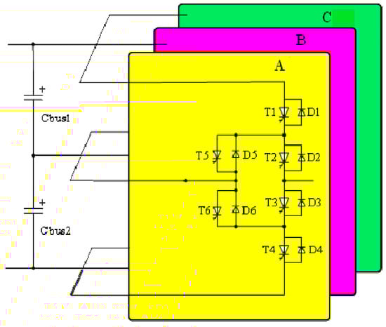
Figure 1.
Three-phase ANPC converter topology. (Letters A, B, C denote the three-phase output terminals).
Compared to the NPC topology, the ANPC converter uses fully controlled power devices, such as IGCTs, as clamping devices, and is equipped with anti-parallel freewheeling diodes, allowing for it to output three voltage levels: positive (P), negative (N), and zero (O). Since the clamping current has bidirectional flow capability, the ANPC inverter has four possible zero-voltage current paths, denoted as OU1, OU2, OL1, and OL2. By appropriately selecting one of these four zero-voltage current paths, it is possible to effectively balance the losses and junction temperatures of the power devices.
2.2. Switching State
According to different switching states and current flow paths, six states can be achieved, which are shown in Table 1.

Table 1.
ANPC three-level converter switching states.
The switching states and current paths for each state are described as follows:
State 1: Positive level and output current greater than zero
IGCT T1 and T2 are turned on, and T6 is also ON. The current is output from the positive bus through the IGCT T1 and T2, as shown in Figure 2a.
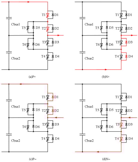
Figure 2.
Current paths in positive and negative level.
State 2: Negative level and output current greater than zero
IGCT T3 and T4 are turned on, and T5 is also ON. The current is output from the positive bus through the FWD D3 and D4, as shown in Figure 2b.
State 3: Positive level and output current less than zero
IGCT T1 and T2 are turned on, and T6 is also ON. The current flows from the FWD D1 and D2 to the positive bus, as shown in Figure 2c.
State 4: Negative level and output current less than zero
IGCT T3 and T4 are ON, and T5 is also ON. The current flows from IGCT T3 and T4 to the negative bus, as shown in Figure 2d.
State 5: Zero-level and output current greater than zero
When the current of the ANPC converter is greater than zero in the zero-level state, there are two current flow paths at the same time. The first, current is output from the neutral point of the capacitor through the FWD D5 and the IGCT T2 and is in the zero-level OU1 or OU2 state, as shown in Figure 3a; The second, current is output from the neutral point of the capacitor through the IGCT T6 and the diode D3, and is in the zero-level OL1 or OL2 state, as shown in Figure 3b.
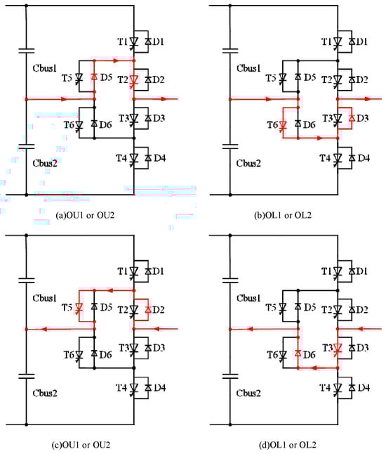
Figure 3.
Current path in zero-level.
State 6: Zero-level and output current less than zero
When the current of the ANPC converter is less than zero in the zero-voltage state, there are two current flow paths at the same time. The first type of current is output from the AC side through the FWD D2 and the IGCT T5 and is in the zero-level OU1 or OU2 state, as shown in Figure 3c; the second, current is output from the AC side through the IGCT T3 and the diode D6 in the zero-level OL1 or OL2 state, as shown in Figure 3d.
For the load current, there are two paths in the ANPC converter when it flows out at the zero state, and there are two paths when it flows in. Therefore, during operation, there are four possible combinations for the flow of load current in and out of the converter. The power losses of the devices vary for each combination. By appropriately distributing the operating time of these combinations, it is possible to achieve loss balancing control of the power devices.
3. ANPC Three-Level Inverter PWM Strategy
3.1. Conventional Modulation Strategy
The introduction of fully controlled power switches T5 and T6 in the ANPC three-level topology enables two bidirectional current paths at zero level states. The two zero-level current paths alternate, allowing for inner switches T2 and T3 to operate in complementary mode instead of being turned on simultaneously. Thus, three-level ANPC can be regarded as a combination of three half-bridge circuits: T1/T5, T2/T3, and T4/T6. Among them, T1 and T6 share the same switching pattern, as do T4 and T5. This ensures that the half-bridge formed by T2/T3 always withstands half of the DC bus voltage.
Conventional PWM schemes for ANPC three-level converters can be categorized into three types: carrier phase-shifting modulation, inner switch frequency modulation, and outer switch fundamental frequency modulation.
In the carrier phase-shift modulation strategy, the three half-bridge circuits operate at equal switching frequencies. The phase difference between the two carriers is 180 degrees, corresponding to the switching of T1 and T2. This separation of drive signals enables alternate operation, reducing switching losses. However, this strategy suffers from relatively poor line voltage harmonic performance. The schematic diagram of the carrier phase-shift modulation strategy is shown in Figure 4a.
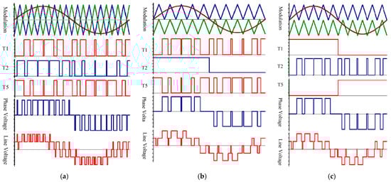
Figure 4.
Conventional PWM strategy. (a) Carrier phase-shifting modulation. (b) Inner switch fundamental frequency modulation. (c) Outer switch fundamental frequency modulation.
To enhance neutral-point balancing and reduce internal switching losses, one PWM method operates the internal switches at the fundamental frequency, while T1, T4, T5, and T6 operate at the carrier frequency. Figure 4b shows the schematic diagram of this modulation strategy. With internal switches modulated at the fundamental frequency, T1 and T5 experience significantly higher switching losses than T2. However, this suppresses the imbalance between internal and external switch losses. Additionally, when the output is at zero voltage, T5 and T6 conduct simultaneously, with each internal switch experiencing half of the load current. This reduces internal switch losses, achieving a balance in power device losses. However, this strategy results in relatively high switching losses for the external switches.
In contrast, another approach operates the external switches at the fundamental frequency, while T2 and T3 operate at the carrier frequency. The schematic diagram of this modulation strategy is shown in Figure 4c. However, this strategy exacerbates the switching losses of the internal switches and fails to address the uneven heating issue between internal and external switches in the three-level ANPC. This PWM strategy is mainly suited for hybrid topologies using SiC and Si devices [27,28].
3.2. Novel Hybrid Fundamental Frequency Modulation
A new PWM optimization strategy, hybrid fundamental frequency modulation, combines the advantages of inner and outer switch fundamental frequency modulation to optimize switching frequency and balance switching losses. The switching states of the converter under this modulation strategy are shown in the Table 2 below.
Table 2.
Hybrid fundamental frequency modulation switching states.
First cycle: When the reference modulation wave is greater than 0, voltage states P and OU2 are used, keeping T2 conducting and T3 off. When the reference modulation wave is less than 0, voltage states N and OL2 are used, keeping T2 off and T3 conducting. Thus, during the first operating cycle, T2 and T3 operate at the fundamental frequency, while T1, T4, T5, and T6 operate at the carrier frequency.
Second cycle: When the reference modulation wave is greater than 0, voltage states P and OL2 are used, keeping T1 and T6 conducting and T4 and T5 off. When the reference modulation wave is less than 0, voltage states N and OU2 are used, keeping T1 and T6 off and T4 and T5 conducting. Thus, during the second operating cycle, T1, T4, T5, and T6 operate at the fundamental frequency, while T2 and T3 operate at the carrier frequency.
In the third and subsequent cycles, the two working states alternate. This strategy equalizes the switching frequencies of internal switches T2 and T3, external switches T1 and T4, and clamping switches T5 and T6, achieving balanced switching losses. This approach resolves the loss imbalance issue observed in the ANPC converter under different modulation strategies. A schematic diagram of the hybrid fundamental frequency modulation strategy is shown in Figure 5.
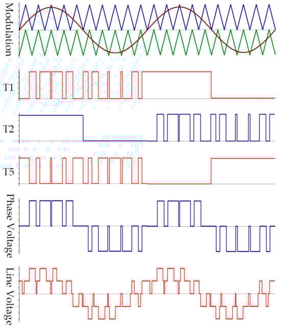
Figure 5.
Hybrid fundamental frequency modulation.
The periodic alternation logic in the proposed strategy follows a fixed, predefined pattern to achieve symmetric loss balancing. By combining inner and outer switch fundamental frequency modulation strategies, the ANPC three-level converter’s switch loss balance can be flexibly optimized. Hybrid fundamental frequency modulation offers multiple application options by tailoring modulation strategies for internal and external switches, effectively addressing uneven heating issues.
4. Loss Calculation Model for ANPC Three-Level Converter
The key parameters at typical junction temperatures of 25 °C and 125 °C can be obtained from the datasheet of the switching devices. Based on these parameters, a loss model for the power devices can be established.
4.1. Loss Calculation for IGBTs
The loss of IGCT consists of conduction loss and switching loss.
Power devices experience conduction losses due to initial saturation voltage drop and conduction resistance. The initial saturation voltage drop and conduction resistance vary approximately linearly with temperature. Therefore, the initial saturation voltage drop, conduction resistance, and conduction losses of power devices can be expressed as follows:
where and denote the initial saturation voltage drop and conduction resistance of the IGCT at a junction temperature of 25 °C, respectively. and are temperature correction coefficients for the IGCT’s initial saturation voltage drop and conduction resistance, respectively. denotes the IGCT junction temperature, and is the instantaneous current flowing through it.
IGCTs incur switching losses during turn-on and turn-off processes. Switching energy losses can be indirectly calculated under test conditions by multiplying voltage and current and integrating over time. The IGCT datasheet typically provides a curve showing the variation of switching energy losses with load current under test voltage conditions at a junction temperature of 125 °C. Energy losses under varying voltages and junction temperatures can be corrected using power functions of the ratios between actual and test voltages and junction temperatures. Therefore, the switching energy loss of an IGCT can be expressed as
where , , and are quadratic fitting coefficients representing the variation of switching energy loss with current under test conditions. and are correction factors for the test voltage and junction temperature (typically 125 °C), respectively. is the actual voltage across the device.
The IGCT average switching loss per cycle is
where is the switching frequency.
4.2. Loss Calculation for Diodes
Similar to the IGCT, the losses of the diode consist of conduction loss and reverse recovery loss:
The initial saturation voltage drop, on-resistance, and conduction loss of the diode can be expressed, respectively, as
where and denote the diode’s initial saturation voltage drop and conduction resistance at a junction temperature of 25 °C. and are the temperature correction coefficients for the diode’s initial saturation voltage drop and conduction resistance. denotes the diode’s junction temperature, and III is the instantaneous current through it.
Fast recovery diodes have negligible turn-on losses, which are typically ignored. However, they incur reverse recovery losses during turn-off. Similar to the IGCT, the diode’s switching energy losses are expressed using parameters from its datasheet as follows:
where , , and are quadratic fitting coefficients representing switching energy loss variation with current under test conditions. is the correction factor for the test voltage ; is the correction factor for the test junction temperature .
The average switching loss of the diode per switching cycle is
5. Loss Analysis of Modulation Strategies
5.1. Switching Loss Distribution for Different Modulation Strategies
The waveforms of voltage and current during a modulation cycle are shown in Figure 6, where φ represents the power factor angle. A modulation cycle is divided into four regions based on the zero-crossing points of the current and voltage. With the current as the reference sinusoidal waveform, the voltage waveform exhibits a power factor angle.
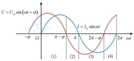
Figure 6.
Voltage and current waveforms during a modulation cycle. Regions (1)–(4) indicate four intervals within a full modulation cycle, segmented by the zero-crossing points of voltage and current, corresponding to different switching or control states discussed in the main text.
Due to the symmetry of the ANPC converter’s upper and lower bridge arms, the analysis focuses on the power devices of the upper bridge arm. Let . Table 3 lists the duty cycles of each switching device in the ANPC three-level converter under different conduction angles.
Table 3.
Duty cycle of ANPC three-level converter switching devices.
5.2. Comparison of Losses in Different Modulation Strategies
The system loss calculation formula is applied to a practical 10 MW-level ANPC three-level converter for verification. The typical parameters of the IGCT and the antiparallel diode selected for the calculation are shown in Table 4 and Table 5.
Table 4.
Typical parameters of the IGCT.
Table 5.
Typical parameters of the antiparallel diode.
With an AC rated voltage of 3300 V, a DC rated voltage of 5000 V, and a rated power factor of 0.95, the RMS and peak AC current values are 1842 A and 2605 A, respectively. Each power device is subjected to half of the DC voltage (2500 V). Owing to the symmetry of the bridge arms, the loss calculation formulas for IGCT devices (e.g., T1/T4, T2/T3, T5/T6) are identical. Similarly, the loss calculation formulas for diodes (D1/D4, D2/D3, D5/D6) are identical. As the loss formulas for all six bridge arms are identical, the total loss of the three-phase ANPC is six times the single-phase loss.
With a power factor of 0.95 and a fixed carrier frequency of 750 Hz, the total losses and loss distribution for three modulation strategies—carrier phase-shift, inner switch fundamental frequency, and hybrid fundamental frequency modulation—are compared.
Table 6 presents the calculated device losses for the three modulation strategies under a power factor of 0.95 and a carrier frequency of 750 Hz. The total losses for the three modulation strategies are 62,251.8 W, 37,044.6 W, and 37,365 W, respectively. With an equivalent switching frequency twice the carrier frequency, the total loss in carrier phase-shift modulation is significantly higher than in the other two strategies. Quantitative analysis shows that the total loss under hybrid fundamental frequency modulation is reduced by 39.98% compared to the carrier phase shift method. The total losses of inner switch and hybrid fundamental frequency modulation are comparable. However, in inner switch fundamental frequency modulation, T1 has the highest loss at 3018 W. In hybrid fundamental frequency modulation, T2 has the highest loss at 2354 W, lower than 3018 W.
Table 6.
Typical parameters of the antiparallel diode (unit: W).
To further analyze the loss distribution under the three modulation strategies, bar charts in Figure 7 compare device types and loss categories.
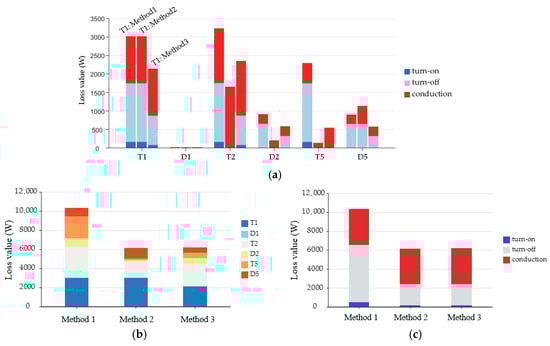
Figure 7.
Losses in a half bridge arm module for three modulation methods. (a) Comparison of loss types of different devices. (b) Comparison of losses of various devices. (c) Comparison of the different types of losses.
The chart shows that in the carrier phase-shift modulation strategy, turn-off losses dominate, while in inner switch fundamental frequency and hybrid fundamental frequency modulation strategies, conduction losses are the largest proportion. In the carrier phase-shift modulation strategy, losses in IGCT devices like T1, T2, and T5 are relatively uniform, simplifying heat sink design. However, its total losses are significantly higher than those of the other strategies, making carrier phase-shift modulation less favorable.
As the total losses in inner switch and hybrid fundamental frequency modulation are similar, the focus shifts to individual device loss distribution. For inner switch fundamental frequency modulation, T2 incurs a loss of 1656 W, while T1 incurs 3018 W, significantly higher than T2. In contrast, in hybrid fundamental frequency modulation, T1 and T2 experience losses of 2145 W and 2354 W, showing a more balanced distribution.
Additionally, in inner switch fundamental frequency modulation, most switching losses of T5 and D5 are borne by D5, totaling 1140 W. In hybrid fundamental frequency modulation, T5 and D5 incur losses of 511.2 W and 580.6 W, respectively, showing a more uniform distribution. A statistical analysis framework based on the coefficient of variation (CV) is developed to quantitatively assess the loss-balancing performance of the two modulation strategies. Calculation results show that with inner switch fundamental frequency modulation, the CV of power switch loss distribution is 1.04. In contrast, the proposed hybrid fundamental frequency modulation reduces this value to 0.85. Comparative analysis shows that the proposed strategy enhances loss balancing by 18.27% over the conventional approach.
Therefore, compared to carrier phase-shift modulation, inner switch fundamental frequency modulation reduces inner switches and overall device losses. Hybrid fundamental frequency modulation further balances device losses compared to inner switch fundamental frequency modulation, addressing uneven heating and improving ANPC converter reliability.
5.3. Effect of Power Factor and Carrier Frequency
The rated parameters of the ANPC converter and typical parameters of the IGCT and reverse parallel diode are consistent with the previous section. A further analysis focuses on device losses under hybrid fundamental frequency modulation, specifically examining the effects of power factor and carrier frequency on total losses and loss distribution.
Table 7 presents calculated device losses for switching frequencies from 350 Hz to 950 Hz at a fixed power factor of 0.95. Table 8 presents calculated device losses for power factors from 0.93 to 0.99 at a fixed switching frequency of 750 Hz. The tables examine how switching frequency and power factor affect device losses, efficiency, and performance of the ANPC converter under hybrid fundamental frequency modulation.
Table 7.
Calculated device losses for a half bridge arm module with a constant power factor of 0.95 and switching frequencies from 350 Hz to 950 Hz (unit: W).
Table 8.
Calculated device losses for a half bridge arm module with a constant switching frequency of 750 Hz and power factor from0.93 to 0.99 (unit: W).
For visual comparison, the data from the above table is plotted in a bar chart graph Figure 8 and Figure 9.
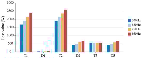
Figure 8.
Comparison of losses at different switching frequencies with constant power factor 0.95.
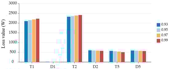
Figure 9.
Comparison of losses at different power factor with constant switching frequency of 750 Hz.
Figures and tables show that in hybrid fundamental frequency modulation, current primarily flows through T1, T2, D2, T5, and D5. This occurs because in inner switch mode, load current flows through T2 and D5 at zero voltage level, while in outer switch mode, it flows through D2 and T5. In hybrid fundamental frequency modulation, T2 incurs the highest switching loss of 2588 W. Additionally, at a switching frequency of 750 Hz and a power factor of 0.95, device losses achieve optimal total loss and loss distribution.
In summary, the proposed hybrid fundamental frequency modulation significantly improves loss distribution and reduces total system losses. It achieves up to 39.98% lower losses than carrier phase-shift modulation and enhances loss balance by 18.27% compared to inner switch modulation. Furthermore, sensitivity analyses under varying power factors and switching frequencies confirm that the hybrid fundamental frequency modulation maintains stable and efficient performance across typical operating conditions. These results demonstrate the method’s effectiveness in improving loss balance and enhancing the reliability of high-power ANPC converters, making it a promising design solution.
6. Simulation and Experimental Results
6.1. Simulation Results
A MATLAB/Simulink (R2018a) simulation model of the ANPC three-level inverter was developed to verify the control effectiveness of the hybrid fundamental frequency modulation strategy, with parameters listed in Table 9.
Table 9.
Parameters of ANPC converter simulation model.
Figure 10a–c show the triggering signals for switches T1, T2, and T5 during the hybrid fundamental frequency modulation. As shown in Figure 10a–c, the inner switch modulation strategy is applied during the first cycle. When the reference modulation wave exceeds 0, T2 remains on, and T3 is off. When the reference modulation wave is below 0, T2 turns off, and T3 turns on. Therefore, in the first cycle, T2 and T3 operate at a fundamental frequency of 50 Hz, while T1, T4, T5, and T6 operate at a carrier frequency of 1000 Hz. In the second cycle, the outer switch modulation strategy is applied, where T1, T4, T5, and T6 operate at 50 Hz, and T2 and T3 at 1000 Hz.
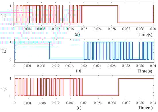
Figure 10.
Simulation verification of switching states. (a) Switching state of T1; (b) Switching state of T2; (c) Switching state of T5.
Figure 11 illustrates current waveforms through various devices under the hybrid fundamental frequency modulation strategy. Figure 11a depicts the current waveform of T1 and D1. The figure shows that in both inner and outer switch fundamental frequency modes, when the modulation wave exceeds 0 and the output is positive, current flows continuously through T1.
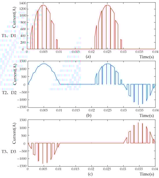
Figure 11.
Simulation verification of current waveforms. (a) Current through T1 and diode D1; (b) Current through T2 and diode D2; (c) Current through T3 and diode D3.
Figure 11b depicts the current waveform of T2 and D2. It can be seen that in the inner switch fundamental frequency mode, the current flows through T2 when the modulation wave exceeds 0. In the outer switch fundamental frequency mode, current flows through T2 when the modulation wave exceeds 0 and the output is positive, and through D2 when the wave is below 0 and the output is zero.
Figure 11c depicts the current waveform of T5 and D5. In the inner switch fundamental frequency mode, current flows through D5 when the modulation wave exceeds 0 and the output is zero. In the outer switch fundamental frequency mode, current flows through T5 when the modulation wave is below 0 and the output is zero.
6.2. Experimental Results
To validate the proposed modulation strategy under practical conditions, a three-level ANPC power converter test platform was constructed to conduct two-phase power cycling tests, as shown in Figure 12. The setup is designed to evaluate the switching performance and losses of the integrated gate-commutated thyristor (IGCT) under rated power conditions, as well as to verify the device’s reliability under its operating voltage, current, and thermal stress.
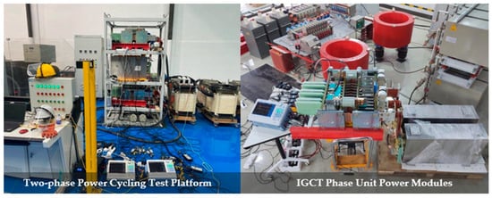
Figure 12.
Experimental setup.
The detailed circuit configuration of the experimental test setup for ANPC power module power cycling tests is illustrated in Figure 13. The core of this platform integrated two structurally identical ANPC power modules within the same test cabinet, operating in rectifier mode and inverter mode, respectively, thereby constituting a back-to-back power recirculation test platform. By connecting a load reactor between the AC output terminals of the two modules, a reactive power exchange channel was intentionally established, thus enabling active power to circulate in a closed loop between the modules. This arrangement simulated the electrothermal stresses imposed on the modules under actual high-power operating conditions. The external DC power supply was only required to provide the total power losses generated during system operation (primarily including switching losses, conduction losses of power devices, and line losses), which sufficed to maintain stable operation of the entire test platform. Consequently, this enabled efficient and economical stable and controllable testing of ANPC power modules under conditions approaching rated power levels.
Figure 13.
Two-phase power cycling test circuit topology.
The system’s rated values are provided in Table 9. The testing protocol initiated with no-load verification by disconnecting the load reactor while progressively elevating the DC-link voltage to ±5000 V and modulation index to 0.95. As illustrated in Figure 14, the inverter output voltage demonstrated a stable three-level waveform under no-load conditions, with no observable overshoot, oscillation, voltage spikes, or current discontinuity, confirming proper IGCT operation. Subsequently, the system commenced loaded testing at 10% rated power with load reactor engaged. Through controlled phase-shift angle and modulation depth adjustments, full-rated operation was achieved. Critical waveforms captured at rated conditions (phase-shift: ) in Figure 15 exhibit 2500 V blocking voltage sustained by both IGCTs and freewheeling diodes, along with load reactor current peaking at 2600 A.
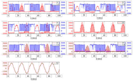
Figure 14.
No-load output characteristics of inverter unit at 5000 V DC-link.
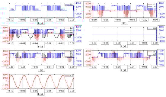
Figure 15.
Coordinated waveforms of rectifier–inverter pair under rated operation.
Figure 14 characterizes the inverter power unit’s no-load output, confirming baseline switching performance. Figure 15 captures coordinated operation of both units: inverter unit IGCT waveforms demonstrate active power regulation, while rectifier unit diode waveforms validate reverse recovery stress during power recirculation. The load reactor current quantifies internal power transfer magnitude. Governed by the proposed hybrid fundamental frequency modulation, the power switches cyclically alternated between inner switch and outer switch fundamental frequency modes. In both operating modes, the output current waveforms were analyzed using MATLAB’s FFT function. The calculated total harmonic distortion (THD) was below 3% in each case, confirming acceptable waveform quality. The measured output power was calculated using the standard three-phase power formula , where , , and . Compared to the rated power of 10 MW, the output power deviation remained within 0.8%. These results collectively demonstrate the operational feasibility of the proposed modulation strategy under high-power conditions.
To further validate the effectiveness of the proposed hybrid fundamental frequency modulation strategy, a systematic comparison between simulation and experimental results was conducted. The simulated switching waveforms (Figure 10) clearly demonstrate the intended cyclic alternation between inner and outer power switches throughout the modulation cycle. This behavior is highly consistent with the experimentally measured IGCT gate signals (Figure 14), particularly the alternating switching activities of devices –, confirming the correct hardware implementation of the hybrid modulation logic. Regarding the current conduction paths, the simulated waveforms of T1/D1, T2/D2, and T3/D3 (Figure 11) verify the expected conduction patterns under different operating modes, which are further supported by the experimental load current waveform (), showing smooth sinusoidal shape and stable phase relationships. As shown in Table 10, in terms of output voltage waveform quality, the simulation under ideal switching conditions yields clean three-level outputs, while the experimental results exhibit the same three-level structure with minor voltage overshoot (200–300 V) and waveform jitter during switching transients. These discrepancies are primarily attributed to parasitic inductance in the power loop, gate driver delays, and snubber circuit dynamics in the physical system. For current ripple, the simulation demonstrates minimal ripple due to ideal filtering, whereas the experimental results show moderate ripple under no-load or light-load conditions, caused by practical filter limitations and switching noise coupling.
Table 10.
Comparison of Simulation and Experimental Results.
The comparative analysis reveals strong consistency between simulation and experimental platforms in terms of switching sequence, conduction behavior, waveform symmetry, and output performance. Furthermore, by integrating electrothermal models and parasitic parameters into the simulation, the model also provides credible estimations of internal losses that are difficult to measure directly in physical tests. This comparison confirms the practical feasibility of the proposed hybrid fundamental frequency modulation strategy.
7. Conclusions
This paper proposed a novel hybrid fundamental frequency modulation strategy for the three-level active neutral-point clamped (ANPC) inverter, aiming to achieve balanced switching operation among power devices. The proposed strategy addresses the issue of unequal loss distribution and localized thermal stress inherent in conventional modulation methods by alternating the roles of inner and outer switches on a cycle-by-cycle basis. This design enables loss equalization without increasing control complexity. Simulation and experimental results validated the effectiveness of the proposed method. Compared to conventional carrier-based and single-mode fundamental frequency modulation strategies, the hybrid approach reduced total system power loss by up to 39.98% and improved the loss-balancing index by 18.27%, which could enhance converter reliability in high-capacity variable-speed pumped storage systems. Future research may focus on the adaptive modulation strategies that respond to real-time thermal feedback, integration with advanced digital controllers for improved responsiveness, and the extension of the proposed method to other multilevel converter topologies and emerging power semiconductor technologies.
Author Contributions
Conceptualization, L.L. and Y.M.; Methodology, L.L.; Software, T.L.; Validation, L.L. and T.L.; Formal analysis, L.L., T.L. and Y.L.; Investigation, Y.W., T.L. and K.G.; Resources, Y.L. and K.G.; Data curation, Y.W., Y.L. and K.G.; Writing—original draft, Y.W.; Writing—review & editing, Y.M.; Visualization, Y.W.; Supervision, Y.M.; Project administration, Y.M.; Funding acquisition, Y.M. All authors have read and agreed to the published version of the manuscript.
Funding
This research received no external funding.
Data Availability Statement
Data are contained within the article.
Conflicts of Interest
One of the authors is a graduate student at Huazhong University of Science and Technology. The remaining authors were employed by the company China Southern Power Grid Energy Storage Co., Ltd. The authors declare that the research was conducted in the absence of any commercial or financial relationships that could be construed as a potential conflict of interest.
References
- Xie, X.; Ma, N.; Liu, W.; Zhao, W.; Xu, P.; Li, H. Functions of energy storage in renewable energy dominated power systems: Review and prospect. Proc. CSEE 2023, 43, 158–169. [Google Scholar]
- Shu, Y.; Chen, G.; He, J.; Zhang, F. Building a new electric power system based on new energy sources. Strateg. Study Chin. Acad. Eng. 2021, 23, 61–69. [Google Scholar] [CrossRef]
- Wang, T.; Zhao, J.; Wang, C. Demand Analysis of Variable Speed Units of Pumped-storage Power Station In Power Grid of China. Water Power 2016, 42, 107–114. [Google Scholar]
- Peng, Y.; Yang, Y.; Chen, M.; Wang, X.; Xiong, Y.; Wang, M.; Li, Y.; Zhao, B. Value Evaluation Method for Pumped Storage in the New Power System. Chin. J. Electr. Eng. 2023, 9, 26–38. [Google Scholar] [CrossRef]
- Liu, P.; Liang, L.; Fan, J. The role and development of the pumped storage power station in electric power system. Hydropower New Energy 2016, 11, 18–20. [Google Scholar]
- Chen, Y.; Xu, W.; Liu, Y.; Mao, Z. Dynamical Response Comparison Between Variable Speed and Synchronous Speed Pumped-Storage Units in Turbine Mode. IEEE Trans. Energy Convers. 2024, 39, 2490–2503. [Google Scholar] [CrossRef]
- Desingu, K.; Selvaraj, R.; Chelliah, T.R.; Khare, D. Effective Utilization of Parallel-Connected Megawatt Three-Level Back-to-Back Power Converters in Variable Speed Pumped Storage Units. IEEE Trans. Ind. Appl. 2019, 55, 6414–6426. [Google Scholar] [CrossRef]
- Afrin, S.; Biswas, S.P.; Mondal, S.; Islam, M.R.; Shah, R. Improved PWM Switching Scheme to Mitigate Power Loss and Switch Temperature of CHB Inverters. IEEE Trans. Appl. Supercond. 2024, 34, 5403105. [Google Scholar] [CrossRef]
- Abeynayake, G.; Li, G.; Joseph, T.; Liang, J.; Ming, W. Reliability and Cost-Oriented Analysis, Comparison and Selection of Multi-Level MVdc Converters. IEEE Trans. Power Deliv. 2021, 36, 3945–3955. [Google Scholar] [CrossRef]
- Nabae, A.; Takahashi, I.; Akagi, H. A neutral-point clamped PWM inverter. IEEE Trans. Ind. Appl. 1981, 1A-17, 518–523. [Google Scholar] [CrossRef]
- Jiao, Y.; Lee, F.C.; Lu, S. Space Vector Modulation for Three-Level NPC Converter With Neutral Point Voltage Balance and Switching Loss Reduction. IEEE Trans. Power Electron. 2014, 29, 5579–5591. [Google Scholar] [CrossRef]
- Senturk, O.S.; Helle, L.; Munk-Nielsen, S.; Rodriguez, P.; Teodorescu, R. Power capability investigation based on electrothermal models of press-pack IGBT three-level NPC and ANPC VSCs for multimegawatt wind turbines. IEEE Trans. Power Electron. 2012, 27, 3195–3206. [Google Scholar] [CrossRef]
- Bruckner, T.; Bernet, S.; Guldner, H. The active NPC converter and its loss-balancing control. IEEE Trans. Ind. Electron. 2005, 52, 855–868. [Google Scholar] [CrossRef]
- Zhang, D.; He, J.; Pan, D. A Megawatt-Scale Medium-Voltage High-Efficiency High Power Density SiC+Si Hybrid Three-Level ANPC Inverter for Aircraft Hybrid-Electric Propulsion Systems. IEEE Trans. Ind. Appl. 2019, 55, 5971–5980. [Google Scholar] [CrossRef]
- Zakzewski, D.; Resalayyan, R.; Khaligh, A. Hybrid Neutral Point Clamped Converter: Review and Comparison to Traditional Topologies. IEEE Trans. Transp. Electrif. 2024, 10, 6087–6099. [Google Scholar] [CrossRef]
- Floricau, D.; Floricau, E.; Dumitrescu, M. Natural doubling of the apparent switching frequency using three-level ANPC converter. In Proceedings of the International School on Nonsinusoidal Currents and Compensation, Lagow, Poland, 10–13 June 2018; pp. 1–6. [Google Scholar]
- Ma, L.; Kerekes, T.; Rodriguez, P.; Jin, X.; Teodorescu, R.; Liserre, M. A new PWM strategy for grid-connected half-bridge active NPC converters with losses distribution balancing mechanism. IEEE Trans. Power Electron. 2015, 30, 5331–5340. [Google Scholar] [CrossRef]
- Yang, J.; Sizhao, L.; Lee, F.C. Switching performance optimization of a high power high frequency three-level active neutral point clamped phase leg. IEEE Trans. Power Electron. 2014, 29, 3255–3266. [Google Scholar]
- Guo, Y.; Gao, X.; Tan, J.; Li, P.; Sun, H. Research on loss balance modulation strategy based on single-phase half-bridge TL-ANPC inverter. In Proceedings of the 5th International Conference on Energy, Electrical and Power Engineering (CEEPE), Chongqing, China, 22–24 April 2022; pp. 375–382. [Google Scholar]
- Jiao, Y.; Lee, F.C. New Modulation Scheme for Three-Level Active Neutral-Point-Clamped Converter with Loss and Stress Reduction. IEEE Trans. Ind. Electron. 2015, 62, 5468–5479. [Google Scholar] [CrossRef]
- Deng, Y.; Li, J.; Shin, K.H.; Viitanen, T.; Saeedifard, M.; Harley, R.G. Improved Modulation Scheme for Loss Balancing of Three-Level Active NPC Converters. IEEE Trans. Power Electron. 2017, 32, 2521–2532. [Google Scholar] [CrossRef]
- Wang, X.; Xiao, H.; Ren, Y.; Cheng, M. A Novel Modulation Strategy for Split-Inductor Active NPC Inverter With Loss Distribution Balancing and Thermal Stress Reduction. IEEE Trans. Power Electron. 2023, 38, 7296–7307. [Google Scholar] [CrossRef]
- Song, W.; He, W.; Zhang, Z.; Ma, C.; Li, J. Active Thermal Control and Power Loss Reduction Scheme for Three-Level Active Neutral-Point-Clamped Inverters With Hybrid Modulation. IEEE J. Emerg. Sel. Top. Power Electron. 2024, 12, 1629–1640. [Google Scholar] [CrossRef]
- Chen, J.; Pei, Y.; Wang, L.; Zhao, Y.; Chen, S. Loss Equalization Strategy of 3L Active Neutral Point Clamped Inverter based on Optimization Algorithm. In Proceedings of the 2024 IEEE 10th International Power Electronics and Motion Control Conference (IPEMC2024-ECCE Asia), Chengdu, China, 17–20 May 2024; pp. 3620–3625. [Google Scholar]
- Joseph, A.; Chelliah, T.R. A Review of Power Electronic Converters for Variable Speed Pumped Storage Plants: Configurations, Operational Challenges, and Future Scopes. IEEE J. Emerg. Sel. Top. Power Electron. 2018, 6, 103–119. [Google Scholar] [CrossRef]
- Busquets-Monge, S.; Nicolas-Apruzzese, J. A Multilevel Active-Clamped Converter Topology—Operating Principle. IEEE Trans. Ind. Electron. 2011, 58, 3868–3878. [Google Scholar] [CrossRef]
- Woldegiorgis, D.; Hossain, M.M.; Wei, Y.; Mhiesan, H.; Mantooth, A. A High Efficiency Three-level Active Neutral Point Clamped Inverter Using Hybrid Si/SiC Switches. In Proceedings of the 2020 IEEE 9th International Power Electronics and Motion Control Conference (IPEMC2020-ECCE Asia), Nanjing, China, 29 November–2 December 2020; pp. 284–289. [Google Scholar]
- Liu, H.; Zhao, T.; Wu, X. Performance Evaluation of Si/SiC Hybrid Switch-Based Three-Level Active Neutral-Point-Clamped Inverter. IEEE Open J. Ind. Appl. 2022, 3, 90–103. [Google Scholar] [CrossRef]
Disclaimer/Publisher’s Note: The statements, opinions and data contained in all publications are solely those of the individual author(s) and contributor(s) and not of MDPI and/or the editor(s). MDPI and/or the editor(s) disclaim responsibility for any injury to people or property resulting from any ideas, methods, instructions or products referred to in the content. |
© 2025 by the authors. Licensee MDPI, Basel, Switzerland. This article is an open access article distributed under the terms and conditions of the Creative Commons Attribution (CC BY) license (https://creativecommons.org/licenses/by/4.0/).