
Screen-Printed 1 × 4 Quasi-Yagi-Uda Antenna Array on Highly Flexible Transparent Substrate for the Emerging 5G Applications


 , and
, and
Abstract
1. Introduction
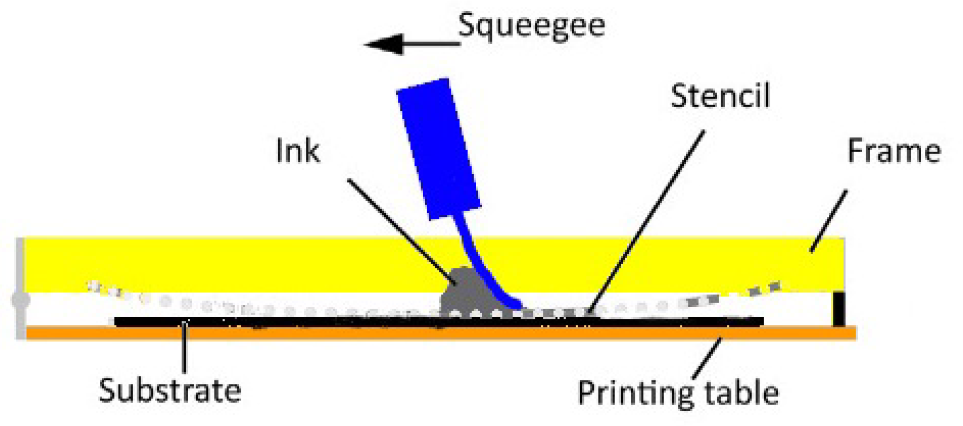
2. Screen-Printing Technique
3. Quasi-Yagi-Uda Antenna
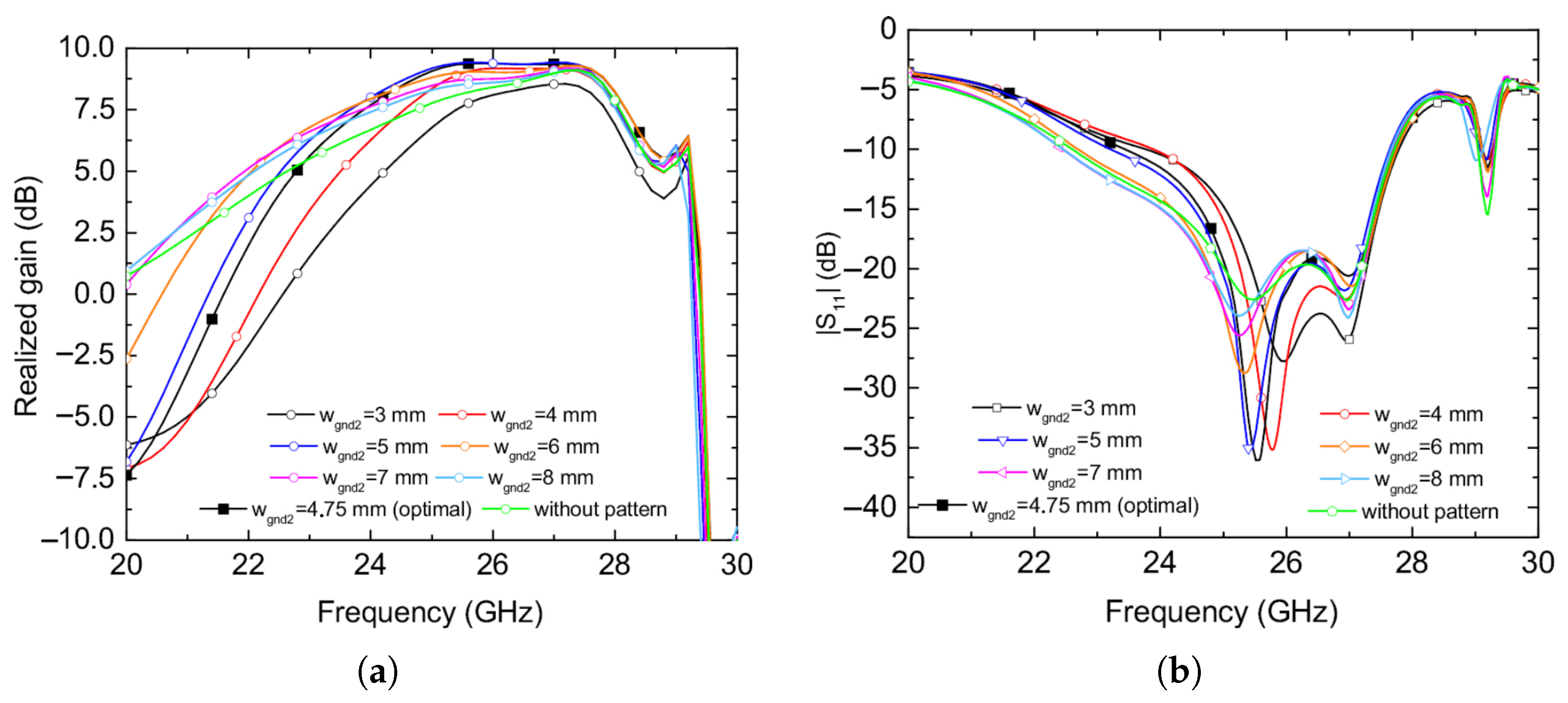
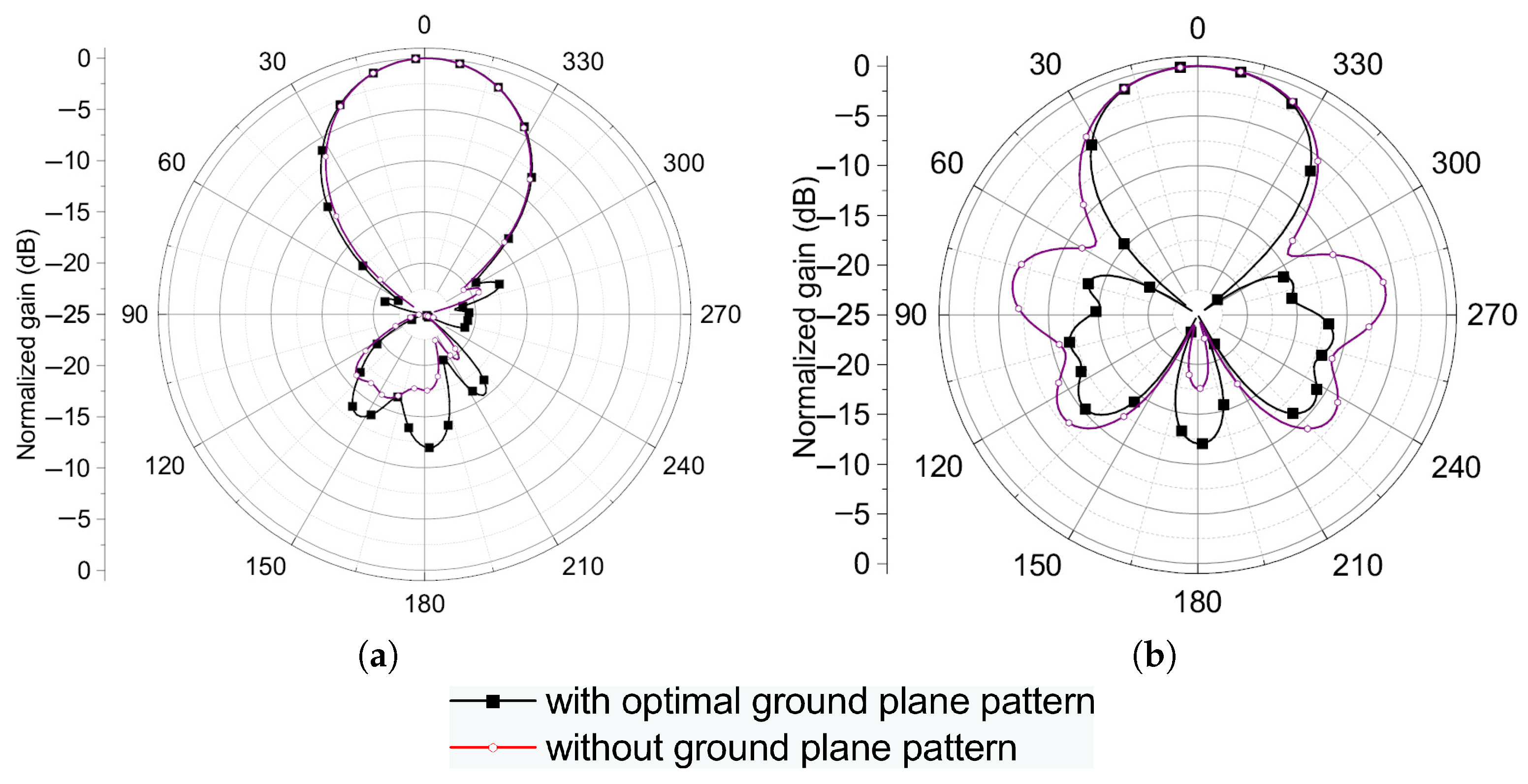
3.1. Design Optimization
3.2. Measurements
3.2.1. Ink and Printed Layer Characterization
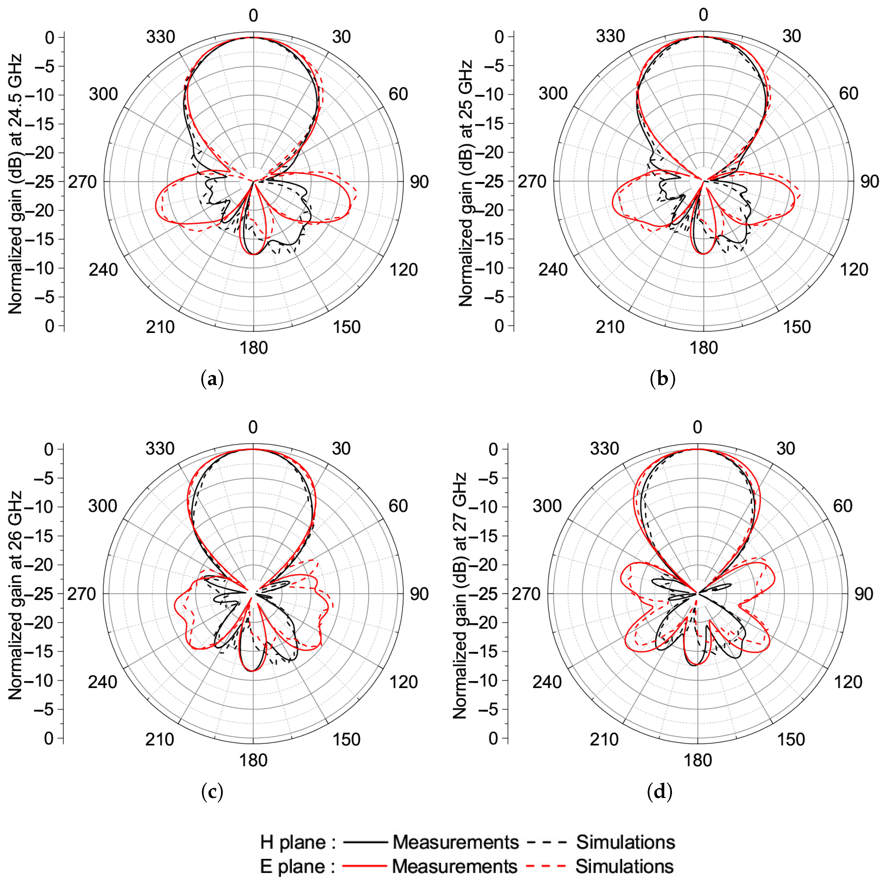
3.2.2. Antenna Measurements
4. Quasi-Yagi-Uda Antenna Array
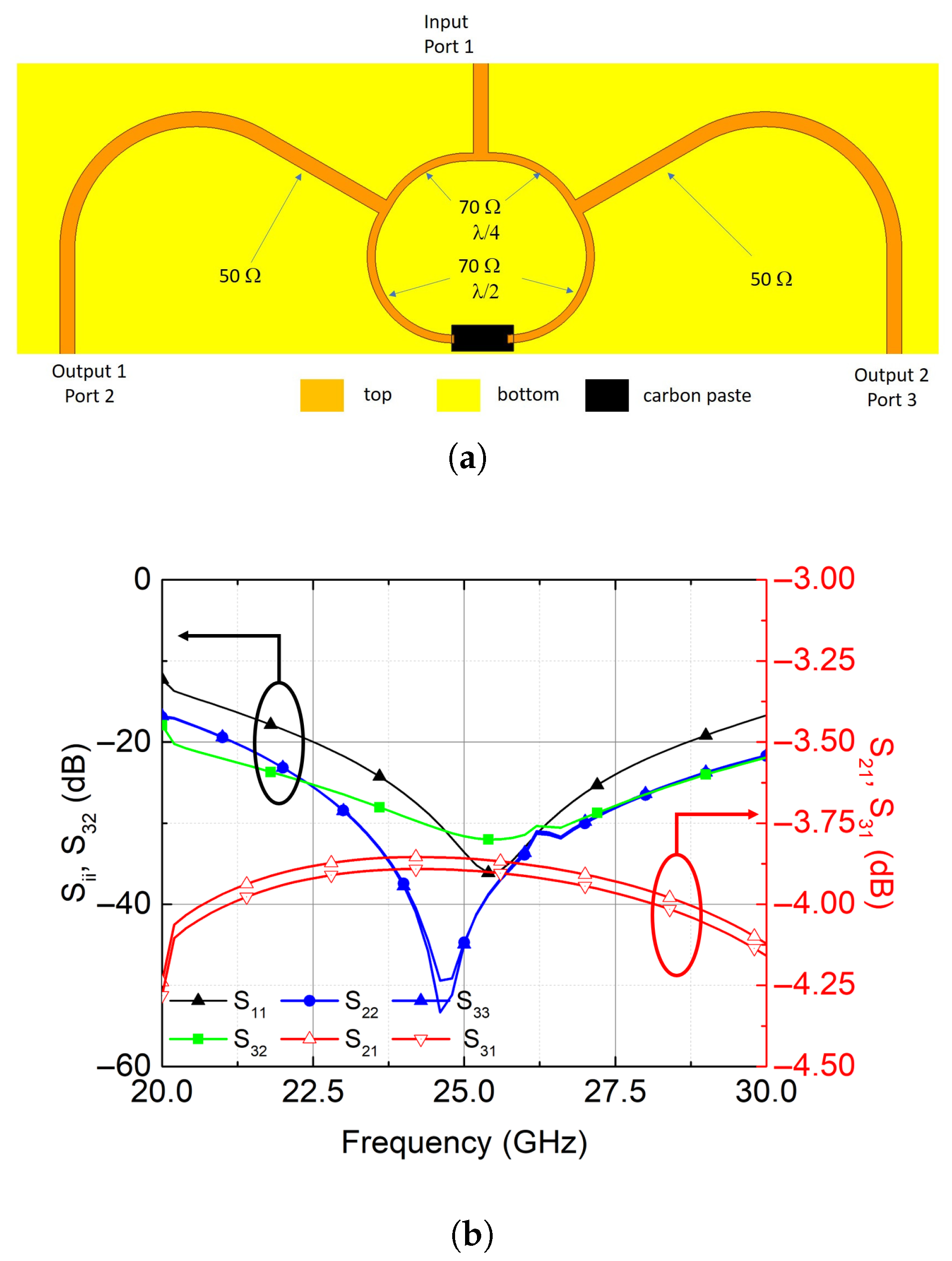
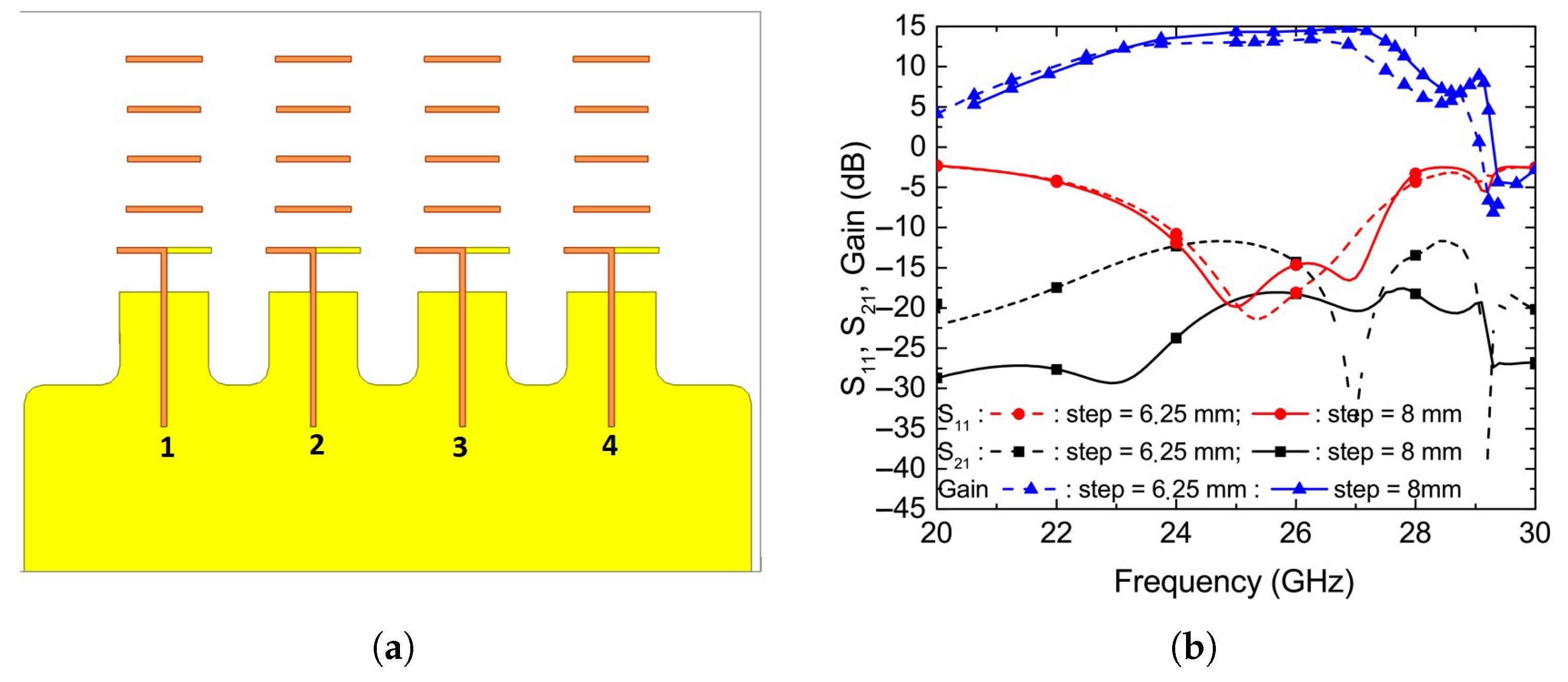
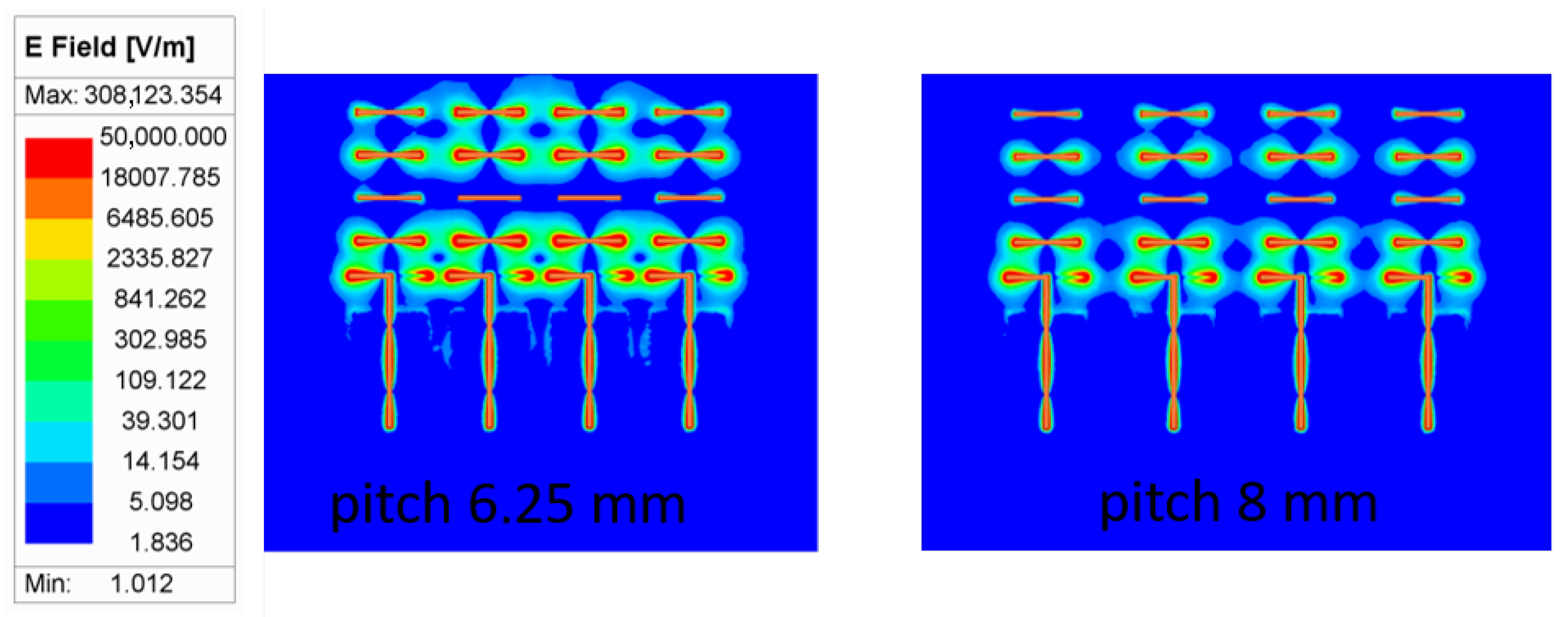
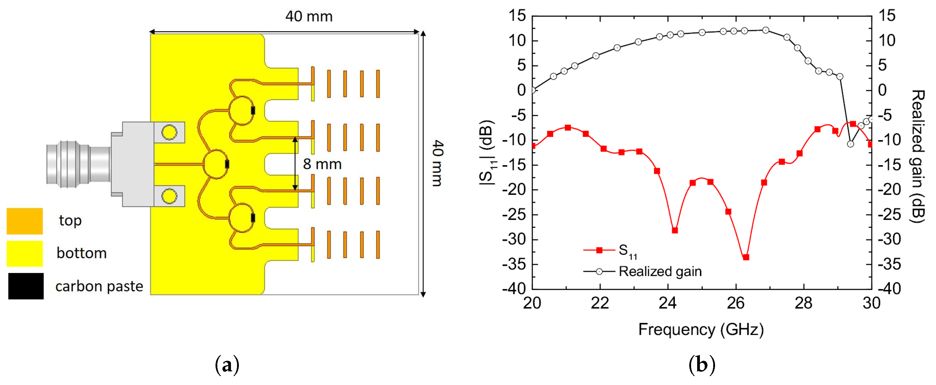
4.1. Design Method
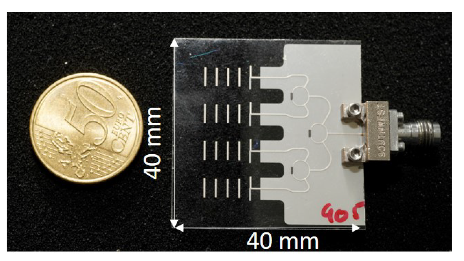
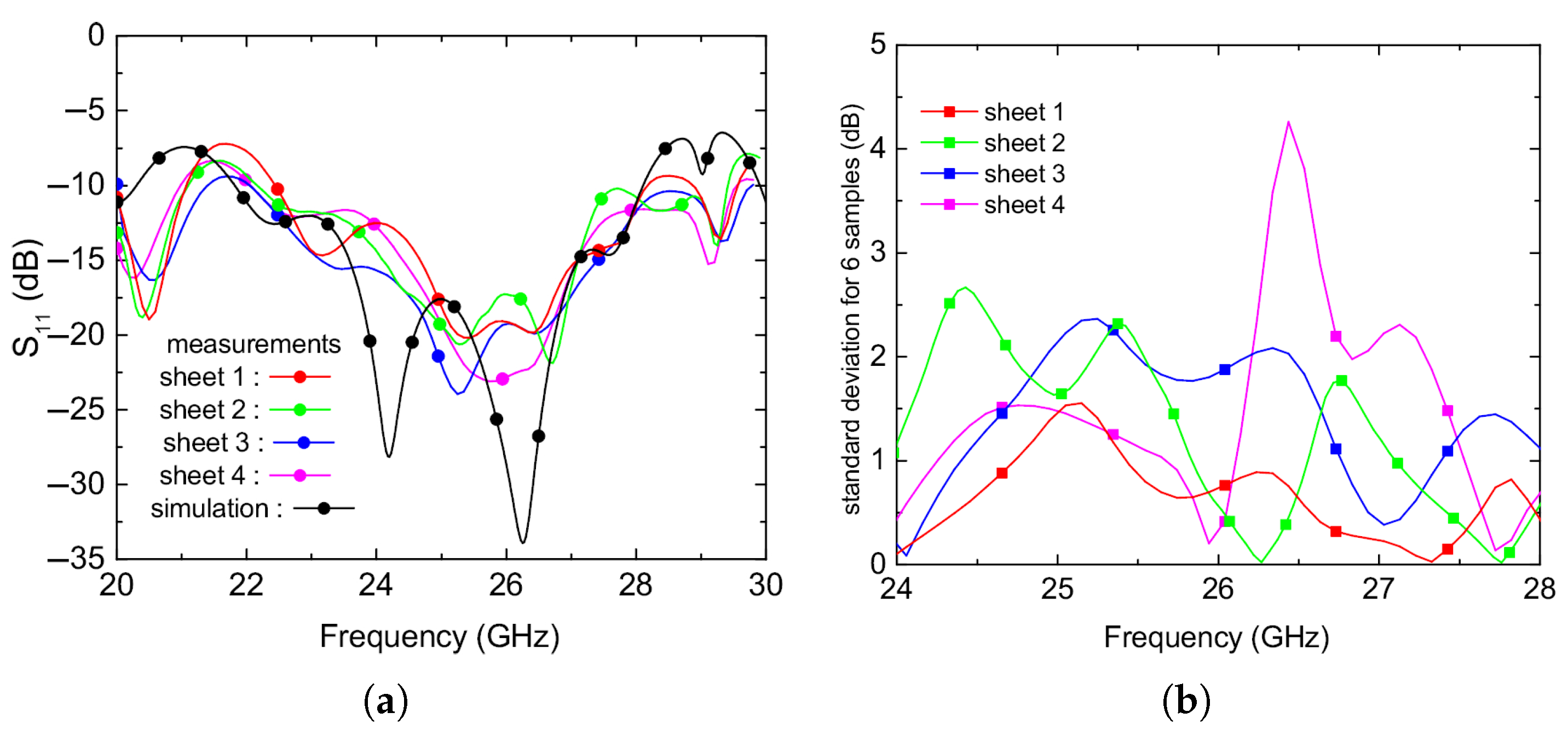
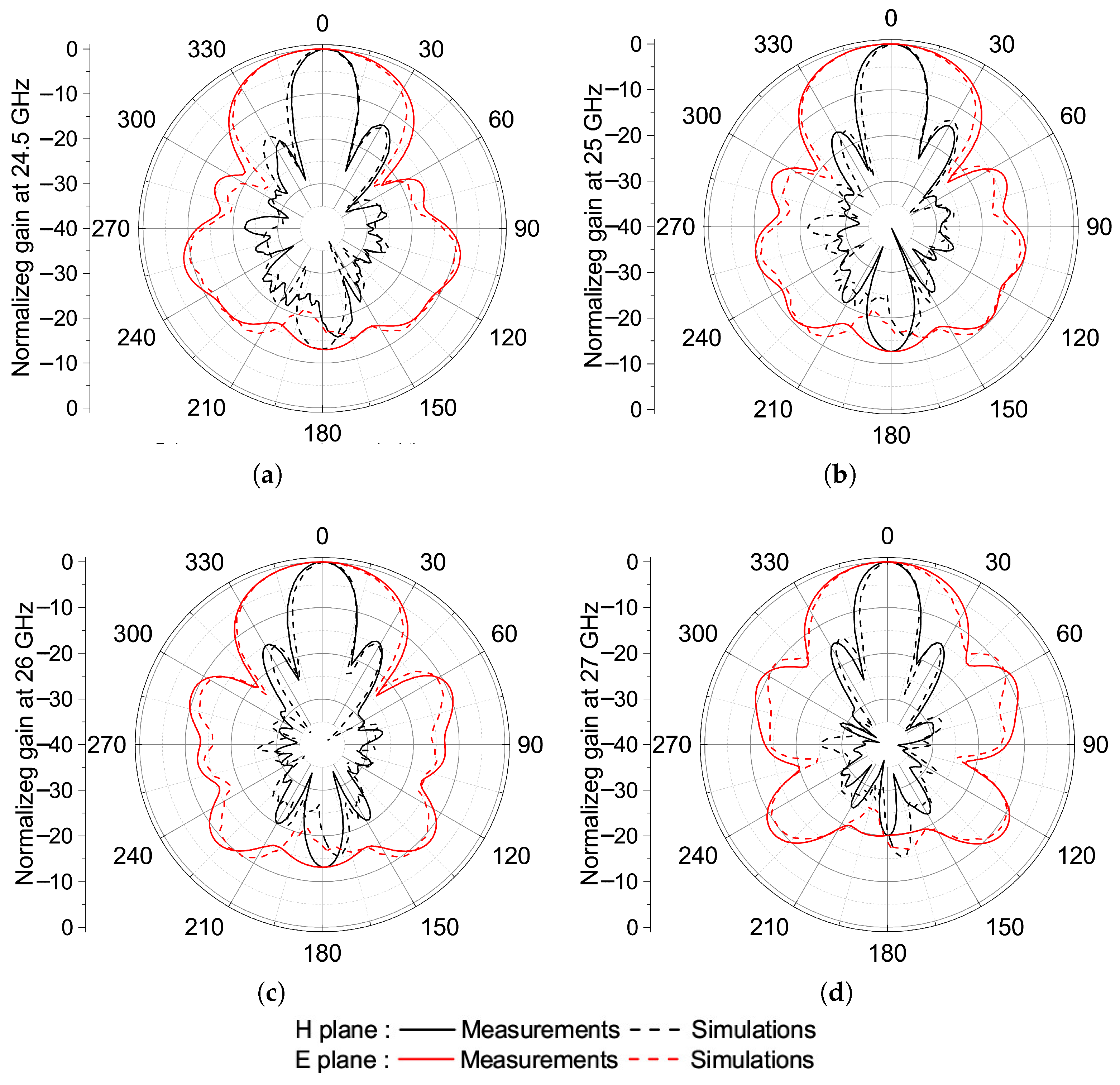
4.2. Measurements
5. Conclusions
Author Contributions
Funding
Data Availability Statement
Acknowledgments
Conflicts of Interest
References
- Sophocleous, M.; Savva, P.; Petrou, M.F.; Atkinson, J.K.; Georgiou, J. A durable, screen-printed sensor for in situ and real-time monitoring of concrete’s electrical resistivity suitable for smart buildings/cities and IoT. IEEE Sens. Lett. 2018, 2, 1501404. [Google Scholar] [CrossRef]
- Claus, N.; Verhaevert, J.; Rogier, H. Comparison of screen-and inkjet-printed meshed wideband antennas for conformal IoT applications. In Proceedings of the 2023 8th International Conference on Smart and Sustainable Technologies (SpliTech), Bol, Croatia, 20–23 June 2023; IEEE: New York, NY, USA, 2023; pp. 1–6. [Google Scholar]
- Simorangkir, R.B.; Gawade, D.R.; Kumar, S.; O’Flynn, B.; Buckley, J.L.; Hannon, T.; Donovan, P.; Newberry, R. Screen printed epidermal antenna for IoT health monitoring. In Proceedings of the 2021 IEEE Asia-Pacific Microwave Conference (APMC), Brisbane, Australia, 28 November–1 December 2021; IEEE: New York, NY, USA, 2021; pp. 395–397. [Google Scholar]
- Hyland, J.S.; Abdullah, S.; Deore, B.; Zhou, W.; Paquet, C.; Xiao, G.G.; Amaya, R.E. Advancement of printed electronics for use in IoT applications and wireless health care devices. In Proceedings of the 2022 IEEE Canadian Conference on Electrical and Computer Engineering (CCECE), Halifax, NS, Canada, 18–20 September 2022; IEEE: New York, NY, USA, 2022; pp. 378–383. [Google Scholar]
- Wagih, M.; Komolafe, A.; Hillier, N. Screen-printable flexible textile-based ultra-broadband millimeter-wave DC-blocking transmission lines based on microstrip-embedded printed capacitors. IEEE J. Microwaves 2021, 2, 162–173. [Google Scholar] [CrossRef]
- Merilampi, S.L.; Björninen, T.; Vuorimäki, A.; Ukkonen, L.; Ruuskanen, P.; Sydänheimo, L. The effect of conductive ink layer thickness on the functioning of printed uhf rfid antennas. Proc. IEEE 2010, 98, 1610–1619. [Google Scholar] [CrossRef]
- Moorthi, A.; Narakathu, B.; Reddy, A.; Eshkeiti, A.; Bohra, H.; Atashbar, M. A novel flexible strain gauge sensor fabricated using screen printing. In Proceedings of the 2012 Sixth International Conference on Sensing Technology (ICST), Limerick, Ireland, 4–6 December 2018; IEEE: New York, NY, USA, 2012; pp. 765–768. [Google Scholar]
- Damalerio, R.B.; Lim, R.Q.; Wee, J.Y.V.; Lim, R.Y.; Cheng, M.-Y. Evaluation of screen printing process in fabrication of small profile conductive ink-based contact force sensor. In Proceedings of the 2023 IEEE 73rd Electronic Components and Technology Conference (ECTC), Orlando, FL, USA, 30 May–2 June 2023; IEEE: New York, NY, USA, 2023; pp. 461–466. [Google Scholar]
- Hasni, U.; Piper, M.E.; Lundquist, J.; Topsakal, E. Screen-printed fabric antennas for wearable applications. IEEE Open J. Antennas Propag. 2021, 2, 591–598. [Google Scholar] [CrossRef]
- Saengchairat, N.; Tran, T.; Chua, C.-K. A review: Additive manufacturing for active electronic components. Virtual Phys. Prototyp. 2017, 12, 31–46. [Google Scholar] [CrossRef]
- Shafer, E.; Kranz, Z.; Watson, A.M. Screen-printed liquid-metal inks for multilayer flexible electronics. In Proceedings of the 2023 IEEE International Conference on Flexible and Printable Sensors and Systems (FLEPS), Boston, MA, USA, 9–12 July 2023; IEEE: New York, NY, USA, 2023; pp. 1–4. [Google Scholar]
- Reuter, K.; Boe, P.; Miek, D.; Höft, M.; Studnitzky, T.; Zhong, C.; Weißgärber, T.; Leon, I.O. 3-D screen printing: Efficient additive manufacturing of groove gap waveguide filters in d-band. IEEE Microw. Wirel. Technol. Lett. 2024, 34, 721–724. [Google Scholar] [CrossRef]
- Akhter, Z.; Li, W.; Yu, Y.; Shamim, A. A fully-screen printed, multi-layer process for bendable mm-wave antennas. In Proceedings of the 2022 16th European Conference on Antennas and Propagation (EuCAP), Madrid, Spain, 27 March–1 April 2022; IEEE: New York, NY, USA, 2022; pp. 1–5. [Google Scholar]
- Lei, H.; Patel, T.; Lopez, J.; MacKenzie, J.D. Screen-printed flexible antennas for 24-ghz ism band and mmwave applications. IEEE J. Flex. Electron. 2025, 4, 138–145. [Google Scholar] [CrossRef]
- Cao, K.; Cheng, K.; Wang, Z. Optimization of screen printing process. In Proceedings of the 2006 7th International Conference on Electronic Packaging Technology, Shanghai, China, 26–29 August 2006; IEEE: New York, NY, USA, 2006; pp. 1–4. [Google Scholar]
- Zeonor Electrical Properties. Available online: https://zeonsmi.com/electronics.html (accessed on 30 September 2010).
- Lukacs, P.; Pietrikova, A.; Vehec, I.; Provazek, P. Influence of various technologies on the quality of ultra-wideband antenna on a polymeric substrate. Polymers 2022, 14, 507. [Google Scholar] [CrossRef] [PubMed]
- Ramos, A.; Varum, T.; Matos, J.N. Compact multilayer yagi-uda based antenna for iot/5g sensors. Sensors 2018, 18, 2914. [Google Scholar] [CrossRef] [PubMed]
- Balanis, C.A. Antenna Theory: Analysis and Design; John Wiley & Sons: Hoboken, NJ, USA, 2015. [Google Scholar]
- Hwang, I.-J.; Ahn, B.; Chae, S.-C.; Yu, J.-W.; Lee, W.-W. Quasi-yagi antenna array with modified folded dipole driver for mmwave 5g cellular devices. IEEE Antennas Wirel. Propag. Lett. 2019, 18, 971–975. [Google Scholar] [CrossRef]
- Nia, B.A.; Flaviis, F.D.; Saadat, S. Flexible quasi-yagi-uda antenna for 5G communication. In Proceedings of the 2021 IEEE International Symposium on Antennas and Propagation and USNC-URSI Radio Science Meeting (APS/URSI), Singapore, 4–10 December 2021; IEEE: New York, NY, USA, 2021; pp. 115–116. [Google Scholar]
- Li, W.; Zhang, H.; Kagita, S.; Shamim, A. All screen-printed, polymer-nanowire based foldable electronics for mm-wave applications. Adv. Mater. Technol. 2021, 6, 2100525. [Google Scholar] [CrossRef]
- Qiu, P.; Feng, Q.; Miyahara, K.; Kanaya, H. Quasi-yagi antenna with parasitic cells and its array for 5g mm-wave operations. Microw. Opt. Technol. Lett. 2022, 64, 117–122. [Google Scholar] [CrossRef]
- Jafarieh, A.; Nouri, M.; Behroozi, H. Optimized 5g-mmw compact yagi-uda antenna based on machine learning methodology. In Proceedings of the 2021 29th Iranian Conference on Electrical Engineering (ICEE), Tehran, Iran, 18–20 May 2021; IEEE: New York, NY, USA, 2021; pp. 751–756. [Google Scholar]
- Wang, D.; Nickel, M.; Schumacher, P.; Polat, E.; Tesmer, H.; Jakoby, R.; Maune, H. A planar quasi yagi-uda antenna designed for liquid crystal based end-fire phased arrays. In Proceedings of the 2021 IEEE Radio and Wireless Symposium (RWS), Virtual, 17–22 January 2021; pp. 164–167. [Google Scholar]
- Luo, Y.; Liu, Y.; Chen, Z.N.; Ma, X.; Yan, N.; An, W.; Ma, K. Millimeter-wave gain-enhanced yagi–uda antenna array with third-order-mode driven dipole and short reflector. IEEE Trans. Antennas Propag. 2024, 72, 1163–1172. [Google Scholar] [CrossRef]
- Korres, A.; Papananos, Y. A broadside yagi-uda antenna with enhanced gain for mm-wave applications. J. Infrared Millim. Terahertz Waves 2025, 46, 17. [Google Scholar] [CrossRef]
- Hammou, D.; Moldovan, E.; Tatu, S.O. Novel MHMIC millimeter wave power divider/combiner. In Proceedings of the 2011 24th Canadian Conference on Electrical and Computer Engineering (CCECE), Niagara Falls, ON, Canada, 8–11 May 2011; IEEE: New York, NY, USA, 2011; pp. 000280–000283. [Google Scholar]


| Ink Name | Conductivity | Thickness | |
| ECI1011 | |||
| Substrate name | thickness | ||
| Zeonor | 2.3 | 0.0009 |
| Parameter | Value | Parameter | Value |
|---|---|---|---|
| d | |||
| Ref | Bandwidth | Gain | Substrate | Metallization | Radiators | |
|---|---|---|---|---|---|---|
| This work | Zeonor | Silver ink | 4 | |||
| [22] | Screen-printable ink | AgNW ink | 1 | |||
| [23] | Megtron6 * | Copper | 4 | |||
| [24] | Neltec NX9240 * | Copper | 5 | |||
| [18] | RO4350B * | Copper | 3 | |||
| [21] | MFLEX * | - | 3 × 2 | |||
| [25] | Liquid crystal | Copper | 3 | |||
| [26] | 8.2% | Ro3010 * | Copper | 2 | ||
| [27] | 15% | ASTRA MT40 * | Copper | 3 × 3 |
Disclaimer/Publisher’s Note: The statements, opinions and data contained in all publications are solely those of the individual author(s) and contributor(s) and not of MDPI and/or the editor(s). MDPI and/or the editor(s) disclaim responsibility for any injury to people or property resulting from any ideas, methods, instructions or products referred to in the content. |
© 2025 by the authors. Licensee MDPI, Basel, Switzerland. This article is an open access article distributed under the terms and conditions of the Creative Commons Attribution (CC BY) license (https://creativecommons.org/licenses/by/4.0/).
Share and Cite
Egels, M.; Venouil, A.; Hannachi, C.; Pannier, P.; Benwadih, M.; Serbutoviez, C. Screen-Printed 1 × 4 Quasi-Yagi-Uda Antenna Array on Highly Flexible Transparent Substrate for the Emerging 5G Applications. Electronics 2025, 14, 2850. https://doi.org/10.3390/electronics14142850
Egels M, Venouil A, Hannachi C, Pannier P, Benwadih M, Serbutoviez C. Screen-Printed 1 × 4 Quasi-Yagi-Uda Antenna Array on Highly Flexible Transparent Substrate for the Emerging 5G Applications. Electronics. 2025; 14(14):2850. https://doi.org/10.3390/electronics14142850
Chicago/Turabian StyleEgels, Matthieu, Anton Venouil, Chaouki Hannachi, Philippe Pannier, Mohammed Benwadih, and Christophe Serbutoviez. 2025. "Screen-Printed 1 × 4 Quasi-Yagi-Uda Antenna Array on Highly Flexible Transparent Substrate for the Emerging 5G Applications" Electronics 14, no. 14: 2850. https://doi.org/10.3390/electronics14142850
APA StyleEgels, M., Venouil, A., Hannachi, C., Pannier, P., Benwadih, M., & Serbutoviez, C. (2025). Screen-Printed 1 × 4 Quasi-Yagi-Uda Antenna Array on Highly Flexible Transparent Substrate for the Emerging 5G Applications. Electronics, 14(14), 2850. https://doi.org/10.3390/electronics14142850