Article

Stability Analysis of Non-Foster Impedance Inverters

1
University of Zagreb Faculty of Electrical Engineering and Computing, Unska 3, 10000 Zagreb, Croatia
2
Končar—Distribution and Special Transformers Inc., Josipa Mokrovića 8, 100090 Zagreb, Croatia
*
Author to whom correspondence should be addressed.
Electronics 2025, 14(13), 2721; https://doi.org/10.3390/electronics14132721 (registering DOI)
Submission received: 31 May 2025 / Revised: 29 June 2025 / Accepted: 30 June 2025 / Published: 5 July 2025
(This article belongs to the Section Microwave and Wireless Communications)

Abstract

Recently, active impedance inverters based on non-Foster negative capacitors have been proposed for applications in widely tunable filters. These designs use a traditional Linvill’s topology of the negative capacitor. Unfortunately, the range of external loads needed for the stable operation of such active inverters is rather limited. However, there is also the negative capacitor based on a recently proposed loss-compensated passive structure. This novel design promises stability-robust behavior for an extremely wide range of external loads. In this study, we compare the stability properties of both approaches and show that the design based on the loss-compensated passive structure is more robust.

1. Introduction

An ideal impedance inverter (K-inverter) is a fictitious two-port device that behaves similarly to a λ/4 transmission line segment (λ being the signal wavelength) with characteristic impedance K. However, the behavior of an ideal K-inverter does not depend on the frequency at all (i.e., it is a dispersionless device) [1,2]. When loaded at the output port with ZL, its input impedance is Zin = K2/ZL, with Zin and ZL being the input and load impedances, respectively, and K being the “transformation” factor. Similarly, an ideal admittance inverter has the “transformation” factor J determined as Yin = J2/YL, with Yin and YL being the input and load admittance. Such inverters are routinely used in multistage filters to isolate neighboring resonators by reducing the loading effect. Due to their ability to convert high impedance/admittance to low impedance/admittance and vice versa, inverters are essential for applications in filter design, phase shifters, antenna matching, artificial transmission lines, and metamaterials [1,2,3,4,5,6].
Here, we focus on the impedance inverter (K inverter), which consists of a T-circuit with three capacitive reactances (Z1 = 1/jωC1, Z2 = 1/jωC2, C1 > 0, C2 < 0, Z2 = −Z1) (Figure 1a,b) [1]. The dual implementation with three inductances (sometimes called an inductive-T “dualizer”) is used for the broadband transformation of small radiation resistance of short dipole antennas to real system impedance [3]. It is important to notice that generic implementations of an impedance inverter (Figure 1a,b) always contain at least an ideal (dispersionless) negative reactive element (negative capacitor or negative inductor). However, such ideal negative elements are physically unrealizable.
A common way to go around this problem is the use of impedance inverter designs in which the negative impedance of physically unrealizable negative elements is “absorbed” by the positive impedance of adjacent stages that contain ordinary elements. Another possibility is to use a transmission line segment or a lumped element whose positive impedance is used to “emulate” a negative shunt capacitance (C2 = −C1 = −1/ω2L) (Figure 1c). Unfortunately, all these implementations suffer from a narrow bandwidth (approximately up to 20% [6]).
Narrow bandwidth is caused by dispersion, as a positive inductance only behaves like a negative capacitance at a single frequency. This is a consequence of the very fundamental Foster theorem, which states that the input reactance/susceptance of every passive and lossless network increases monotonically with frequency [7,8].
On the other hand, there are active electronic circuits that mimic the behavior of hypothetical negative capacitors and negative inductors, the so-called non-Foster (NF) elements [9,10,11,12]. The dispersion function of NF elements can be approximated as the inverse of the dispersion function of ordinary reactive elements [8,13]. For example, the dispersion of the ordinary capacitance can be compensated by the dispersion of the negative capacitance (NC), which significantly improves the bandwidth. Practically speaking, classical non-Foster (NF) elements are based on a special amplifier (the so-called negative impedance converter, NIC) that contains a load to be “negated”, which is located in the positive feedback loop. The superposition of the input signal and the amplified signal being fed back changes the ratio between input voltage and current, resulting in negative input impedance [13,14]. NF elements have been investigated for many years since they can assure the broadband operation of numerous devices such as small antennas [3,15,16,17,18,19,20,21], active metamaterials [8,22,23], active metasurfaces [24,25,26,27,28], amplifiers [29,30,31], voltage controlled oscillators [32,33,34], and phase shifters [35,36,37], to mention a few. The most serious drawback of the NF elements is their proneness to instability, caused by the inevitable use of a positive feedback loop of the associated NIC [38,39,40,41,42,43,44,45,46,47,48,49]. Although significant progress has been achieved in recent years, maintaining stable operation is still a difficult task that prevents the widespread use of NF elements.
Recently, it has been shown that it is possible to use NF elements for the design of active broadband impedance inverters as part of tunable multistage bandpass filters [6,50,51,52,53]. For example, the filters in [6,51] showed a bandwidth of 30% centered at 2.45 GHz and a tunability of up to 50%, which is a remarkable result. However, this broadband tunability was achieved by optimizing the NIC circuit and controlling four design parameters simultaneously. In addition, stability properties have only been tested to a limited extent. Indeed, it was silently presumed that the stability properties of a one-port NF element would be transferred to a two-port device using such an NF element (in this case, an impedance inverter) instead of testing the stability properties of the entire NF-based device.
Furthermore, a new NF passive-structure-based loss-compensated design was also presented recently [54,55,56]. It was demonstrated that these new NF elements can also be used in tunable filters, yielding very good results (20% tunability and 30% bandwidth), but with only two design parameters [55]. A very preliminary study of the stability properties of such a design (with quite a limited range of values of external loading impedances) was published in [56].
To summarize, it appears that NF-based impedance inverters are a promising technology, especially in the context of tunable filters. However, their stability properties are currently unclear.
Here, we analyze the stability properties of a system consisting of an active inverter based on two positive capacitors and an NF shown in Figure 1b, loaded with an external passive network (Figure 2). The NC is implemented in different ways (three different versions of the well-known Linvill’s NIC [14] as well as a recently introduced loss-compensated design based on a passive structure [54,55,56]).
The rest of the paper is organized as follows: Section 2 (Materials and Methods) describes the NF negative capacitors used in the design of the active impedance inverter, whose stability is tested. Section 3 (Results and Discussion) shows the results of the stability analysis, while Section 4 draws the conclusions.

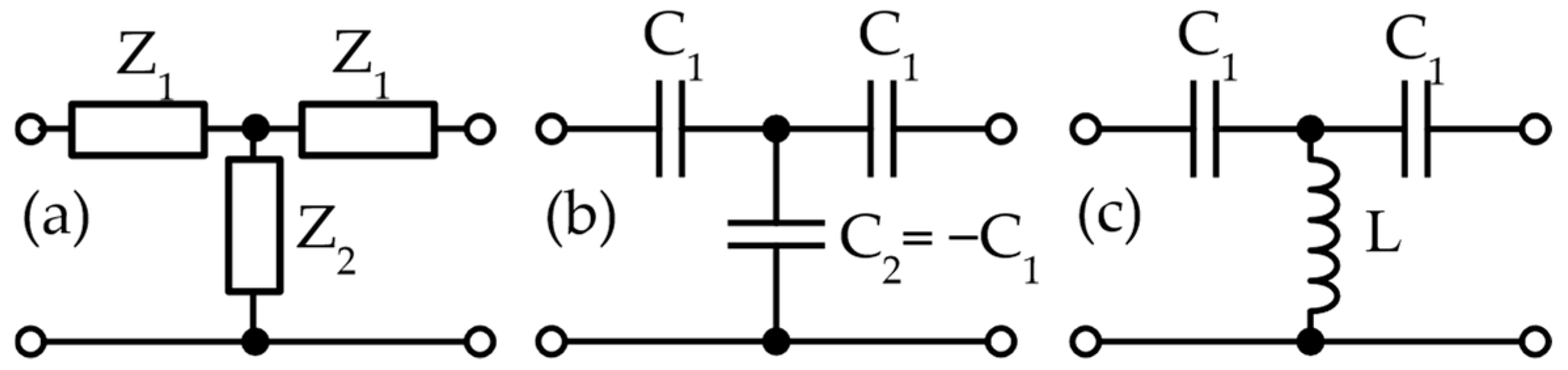
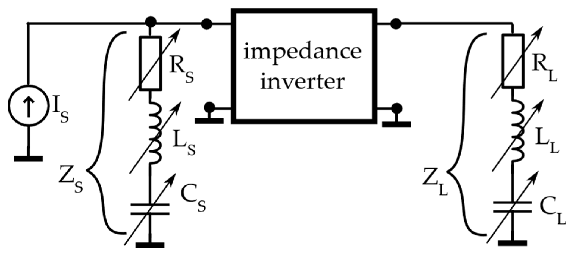
2. Materials and Methods

As mentioned in the Introduction, classical NF negative capacitors are based on reversing the sign of the usual positive reactance through the use of NICs. The simplest NIC implementation contains an ideal voltage amplifier with a voltage gain A and a load (in this case, the simple capacitor CF) that is in a positive feedback loop (Figure 3a) [8,12,14]. A very simple analysis shows that this amplifier reverses the voltage drop across the capacitor, which in turn reverses the direction of the input current, resulting in input capacitance that is a scaled “negative image” of a load capacitance ( C i n = 1 A C F ). In most cases in practice, one chooses A = 2 , resulting in C i n = C F . This simplified explanation presumes that a NIC contains a dispersionless amplifier with an infinite bandwidth. Unfortunately, such a system would clearly not be causal and therefore not physical. The gain in every realistic amplifier decays with frequency and can be described by a general two-pole (2P) dispersion model:
A ω = A 0 1 + j ω / ω p 1 1 + j ω / ω p 2
The term A0 is the gain at very low frequencies, while ωp1 and ωp2 are the angular frequencies of the first and second poles, respectively. There is also a simpler version of (1), the so-called one-pole model (1P), in which ω p 2 . These two models are commonly used in the design and stability predictions of classical NIC-based NF elements [3,11,12,13,15,36]. It is important to mention that one of the well-known Linvill designs from [14] is merely a floating version of the basic principle shown in Figure 3a. The other Linvill designs in [14] use current amplifiers, but the basic principle is again very similar to that shown in Figure 3a and is described by (1). All the above-mentioned implementations provide “negative dispersion”, which is indicative of NF elements (right side of Figure 3a).
Figure 3. (a) The simplest NIC implementation of NF NC based on a positive feedback loop that flips the positive capacitor into a negative capacitor with the comparison of dispersion of positive capacitance (red) and negative equivalent capacitance (green) generated by such a circuit. (b) Passive loss-compensated NF NC. Parallel R-L network with negative-capacitance behavior (Ceq) above the cut-off frequency (ω > R/L) (the behavior of only the reactance (X) is shown in the graph). Equivalent negative capacitance is connected in series with Req, which models the losses. (c) A full model of loss-compensated NF NC, which shows the compensation of losses from the R-L network by a series circuit with negative resistance generated by NIC (RNIC).
Electronics 14 02721 g003
The main difference between the traditional Linvill’s designs and the newly proposed loss-compensated approach [54] is the relaxation of the stability conditions. In Linvill’s approach, the load that is converted to its negative counterpart (using either a one-pole/low-pass or a two-pole/bandpass design) is purely reactive. Simply, as detailed previously, in classical negative-capacitance applications, one uses a lumped capacitor as the load to be “inverted”, which is located in a positive feedback loop. Unfortunately, stability conditions are rather demanding in the presence of purely reactive loads [51,52]. Conversely, in the newly proposed design [54], NC behavior results from a passive parallel RL network. As detailed in [54], that network behaves like a lossy NC above its cut-off frequency (fc = fRL = R/(2πL)) (Figure 3b).
We start with the input impedance of a shunt RL network:
Z R L = R ω 2 ω R L 2 + j R ω ω R L   1 + ω 2 ω R L 2 ,
Here, ωRL = R/L. For the case of high-frequency behavior (ωωRL), one obtains
Z R L ω ω R L R + j R ω ω R L = R + j R 2 ω L = R e q + 1 j ω C e q ,
with Ceq = −L/R. Thus, at the frequencies above fRL, the impedance of the shunt RL network (Figure 3b) shows a negative slope of the reactance X, but with a considerable real part (high losses). This behavior can be modeled as a series connection of the resistance (Req) and a negative capacitance (Ceq < 0). The (unwanted) losses are then compensated by an additionally added series circuit with negative resistance (Figure 3c). This negative resistance is generated by an additional NIC circuit that flips a positive resistance into a negative one, thus achieving a loss-compensated passive NF NC. This design, therefore, shows a band-limited behavior with a very broad operating bandwidth (up to 1:10 [54]). Furthermore, it lowers the Q factor due to the presence of losses, which reduces the sensitivity of the whole circuit, which in turn also improves stability properties.
Essentially, a very good stability robustness is achieved due to the fact that the active part (NIC) performs the negation of only the real load, which is in line with the analysis of the stability of negative resistances [12]. Finally, it should also be mentioned that the novel loss-compensated approach is, in a sense, similar to the NF elements based on loss-compensated negative-group-delay (NGD) networks [57,58]. However, there are two important differences: (i) NF elements based on an NGD approach have a narrower operating bandwidth (1:1.45), due to the inevitable use of RLC resonators; (ii) NF elements based on loss-compensated NGD approach are inherently unidirectional, which seriously limits their applications. We performed stability analysis using four different NC designs. These designs were the “traditional” Linvill’s NIC in one-pole (low-pass) and two-pole (bandpass) configurations from [51], the improved Linvill’s NIC from [6], and the new loss-compensated NF NC design [54,55,56]. The entire stability analysis was performed using linear equivalent circuits that were prepared in two ways. The first three designs were simulated as linear causal circuit-theory models with ideal positive and negative circuit elements from [6,59] for the one- and two-pole NF NC, and from [6] for the improved two-pole NF NC design. The simulation of loss-compensated NF NC was based on a small-signal equivalent circuit extracted from the SPICE model in [55]. This SPICE model had been originally used in [52,55] for Cadence VirtuosoTM simulations of the NIC part in 40 nm TSMC CMOS technology. The newly proposed structure [54,55,56] is inherently a bandpass design (at higher frequencies, the dispersion of the NIC causes the system shown in Figure 3b to behave like a positive inductance). Therefore, we compared it to similar realizations of traditional NF NCs: the one-pole (low-pass) and two-pole (bandpass) designs from [6,51]. To make a fair comparison, we adjusted the NF NC bandwidth from the design in [51] to match the bandwidth from a newly proposed design in [55] (0 GHz to 6.72 GHz for one-pole and 1.34 GHz to 6.72 GHz for both two-pole designs and loss-compensated design, respectively). The impedance inverter transformation factor for the analyzed inverters (K = 1/(ω C 1 ) = 1/(ω C 2 )) was set to 56.48 Ω at 2.45 GHz, with C1 = +1.15 pF and C2 = −1.15 pF [19,23,24]. Furthermore, the stability-improved two-pole Linvill’s NF NC from [6] had K = 44 Ω at 2.45 GHz, with C1 = +1.48 pF and C2 = −1.48 pF.
At first, the impedance inversion of all the mentioned active impedance inverters was cross-checked by circuit-theory simulations in the Keysight ADSTM (version 2024) CAD environment. Then, the stability properties of all four realizations of active impedance inverter, loaded with five different passive networks (Figure 2), were investigated using a two-step process.
In the first step, we used the Amcad Stability Analysis Tool STANTM (version 3.1), which is based on pole-zero identification. We used STANTM as it allows us to work with experimental/measured data, as well as SPICE-based models, when the full model of the system is unknown. Of course, there are other software packages that could have been used for stability analysis. For example, pole-zero identification is available in freeware packages such as Python (using the control systems library) [60] and MATLAB (via the System Identification app) [61].
By investigating the (unstable) RHS poles in the frequency domain of the current transfer function (Iout/Iin) and the impedance function (Vin/Iin), stability maps were obtained, which are presented in Figure 4. A polynomial of a sufficiently high degree was used in order to span the whole range of the two-dimensional parameter space presented in each subfigure of Figure 4.
In the second step, the above results were cross-checked using a Keysight ADSTM transient solver, where the unstable behavior shows an exponential growth of the output voltage (Vout) and current (Iout) in the time domain, while stable behavior was verified by decaying time signals, under impulse excitation.
All simulations were performed with a current source excitation (Figure 2), as the NF NCs used belong to the open-current stable (OCS) types. This is also the reason why we only analyzed the scenario in which the input and output loads were RLC tanks connected in shunt. There are also known implementations of multistage bandpass filters with inverters connected between series tank circuits [6,51,55]. One may conclude that the active inverters in these filters should be of the SCS type. Whether the stability properties are different in these scenarios is currently unclear and would need to be investigated in a separate study.
All tests were conducted using a standard PC (Windows 10, Intel i5 processor with 64 GB of RAM and a 1 TB SSD drive (Intel, Santa Clara, CA, USA)). The settings for the tools used in this study were kept at default values. For all cases, behavior was examined in a range of 1 MHz to 300 GHz (in order to cover frequencies much higher than the operating frequency of several GHz). In ADSTM transient analysis, a sufficient timestep and total length were used in order to assess the increase or decrease in signal behavior. For STANTM, polynomials of a sufficiently high degree were used in order to span the whole range of the 2D parameter sweep up to 300 GHz, in order to achieve a good fit.

3. Results and Discussion

The results obtained by the above-described two-step procedure (pole-zero stability analysis in STANTM and transient simulations in ADSTM) are presented in Figure 4, with all simulation parameters given in the caption. Briefly, two different practical scenarios were analyzed. The case with varied pure real loads RS and RL (Figure 4a–d, second row of Figure 4) represents a realistic scenario of the inverters used as impedance tapers or transformers. In the third row (Figure 4e–h), the resistors RS and RL were varied again, but connected in series with the LC resonant circuit (Figure 2), which simulates the filter scenarios from [6,51,55]. Additional results for the scenario of filters with varying Q factor are shown in the fourth, fifth, and sixth rows in Figure 4. In these cases, the loading capacitance and inductance were varied across a very broad range of values with several different values of fixed resistance. The range of element values used in this parametric analysis was chosen to represent all possible practical scenarios. First, we took the initial values from published designs of practical filters with active impedance inverters [6,51,55]. Then, the range of these values was extended by two orders of magnitude. In this way, all other practical applications with high and low impedance, such as non-Foster-based small dipole antenna and non-Foster-based small loop antenna, are covered by this analysis. The results for the impedance inverter with simple one-pole NF NC (Figure 4a–g, first column) show limited performance. This realization is unstable for pure real loads (Figure 4a), stable in a filter environment (Figure 4e), and unaffected by varying Q factors of external resonant networks (Figure 4i–q). However, this design is rather sensitive. Indeed, any change in loading capacitance larger than 0.699 pF pushes the system into unstable behavior. In the case of the two-pole Linvill’s NF NC-based impedance inverter (Figure 4b–r, second column), the system shows stable behavior only for rather small values of loading external impedances. Unfortunately, this system is unstable over almost the entire range of the K-curve and only shows stable behavior for very large values of the load resistance (Figure 4b,f). Similarly, this system is also stable for low values of external capacitance and inductance, with better stability characteristics for smaller Q factors (Figure 4j–r). In classical broadband filters with low-Q design, the better stability properties observed under a low Q factor are an advantage. The same applies to a low-Q tunable bandpass filter with constant fractional bandwidth. The stability properties improve in the enhanced realization of the two-pole system in [6], which shows that it is possible to achieve stability for a large group of external loads through careful modifications (Figure 4c–s, third column).
Furthermore, we calculated the logarithmic sensitivity [62] of the envelope decay of the impulse response current ( ~ e σ t , σ being the real part of complex frequency s = σ + jw) for the modest-Q case (Figure 4m–p), defined with respect to the value of C at the operating point, which is defined as R = 50 Ω and L = 10 nH. Those values were chosen since most RF systems have a Z0 = 50 Ω, and L = 10 nH was chosen in order to have the same inductance for all four cases of some medium value. The envelope decay of the impulse response current is presented in Figure 5, with calculations of sensitivity (|S| = (σ5% − σ1%)/(C5% − C1%)) presented in Table 1. As expected, this calculation resulted in the lowest sensitivity for the loss-compensated design of NC.
Thus, it can be concluded that the newly proposed passive, loss-compensated design shows an extremely robust stability behavior for all the investigated scenarios, both for real and complex loads, which is evident by consistently stable behavior with changes in all the parameters presented in Figure 4. The summary of the stability analysis of the four different NF NC implementations of impedance inverters from Figure 4 is given in Table 2.
The presented results show several important insights into the design of NF NCs. First, a two-pole bandpass design that eliminates the unstable DC pole [50,52] improves the stability properties of the associated system. Second, the stability properties can be further improved by careful improvement of a “traditional” two-pole Linvill’s NF NC [6]. Third, the largest improvement in stability properties can be achieved by incorporating a loss-compensated passive network into the NC design [55,56]. The physical background of stability robustness is based on the simultaneous application of two different phenomena. The first is the band-limited (high-pass) operation, which prevents the occurrence of an unstable DC pole, and the second is the presence of losses, which, although externally compensated by a negative resistance, reduces the Q factor of the loss.compensated NF NC and thus the overall sensitivity.
Finally, it should be emphasized that the presented stability analysis was performed on the basis of linear equivalent circuits in order to allow for a fair comparison of all the known designs of NF-based impedance inverters. The analysis examines the basic physical phenomena that can cause instability. The focus of this study is on understanding circuit theory models and their influence on stability, not on various technologies that could be used to achieve such systems. It is also assumed that possible influences of the unavoidable parasitics, component tolerances, aging, and temperature variations can be compensated by standard methods such as the use of additional negative feedback and microelectronic technology [6,8,52,63]. The analysis of these technological parameters on the stability characteristics, as well as the practical realization of microelectronic loss-compensated NF NC in CMOS technology, could be a topic of our future study.

4. Conclusions

A numerical investigation of the stability of different realizations of NF-based active impedance inverters was carried out using both a pole-zero analysis and a transient analysis. Both methods showed that the stability properties of the active inverter based on a passive loss-compensated NF structure were superior to those of all “traditional” designs based on Linvill’s NICs. The stability characteristics of the passive loss-compensated NF structure were also significantly better than those of loss-compensated NGD-based designs. Apart from tunable filters, impedance inverters based on loss-compensated NF structures can also be used in other RF systems that require stable behavior across widely varying impedance values. These include, for example, actively matched small broadband antennas and active metamaterials/metasurfaces.

Author Contributions

Conceptualization, B.O. and S.H.; methodology, B.O. and S.H.; software, B.O.; validation, B.O. and S.H.; formal analysis, B.O. and S.H.; investigation, B.O. and S.H.; resources, S.H.; data curation, B.O.; writing—original draft preparation, B.O. and S.H.; writing—review and editing, B.O. and S.H.; visualization, B.O.; supervision, S.H.; project administration, S.H.; funding acquisition, S.H. All authors have read and agreed to the published version of the manuscript.

Funding

Part of this material is based upon the work on the projects “Non-Foster Networks for Tunable and Wideband RF Devices” (EOARD grant FA8655-20-1-7008), “General Stability Theory of Non-Foster and Time-varying Elements” (EOARD grant FA8655-22-1-7055), and “Active and Reconfigurable Electromagnetic Structures and Systems” (HRZZ grant IP 2022-10-2351). The authors especially thank AMCAD Engineering for providing STAN tool used in stability analysis.

Data Availability Statement

The raw data supporting the conclusions of this article will be made available by the authors on request.

Conflicts of Interest

The authors declare no conflicts of interest. Author Boris Okorn was employed by the University of Zagreb Faculty of Electrical Engineering and Computing during the time of this study and is currently employed at Končar—Distribution and Special Transformers Inc.

Abbreviations

The following abbreviations are used in this manuscript:
NFNon-Foster
NCNegative capacitor
NICNegative impedance converter
NGDNegative group delay
OCSOpen-circuit stable
RHSRight-hand side
SCSShort-circuit stable

References

  1. Zverev, J.A.I. Handbook of Filter Synthesis; Wiley: Hoboken, NJ, USA, 2005. [Google Scholar]
  2. Matthaei, G.L.; Young, L.; Jones, E.M.T. Microwave Filters, Impedance-Matching Networks, and Coupling Structure, 2nd ed.; Artech House: Dedham, MA, USA, 1980. [Google Scholar]
  3. Sussman-Fort, S.E.; Rudish, R.M. Non-Foster impedance matching of electrically-small antennas. IEEE Trans. Antennas Propag. 2009, 57, 2230–2241. [Google Scholar] [CrossRef]
  4. Mocanu, I.A. Compact Dual Band Ring Coupler Using Miniaturized Metamaterial Left-Handed Impedance Inverters. IEEE Access 2021, 9, 86119–86131. [Google Scholar] [CrossRef]
  5. Kholodnyak, D.V. Metamaterial transmission lines and their applications. In Proceedings of the 2017 IEEE Conference of Russian Young Researchers in Electrical and Electronic Engineering (EIConRus), St. Petersburg and Moscow, Russia, 1–3 February 2017; pp. 3–8. [Google Scholar]
  6. Kalmykov, N.; Kholodnyak, D. Non-Foster Elements Pave the Way to Design Novel Wideband and Tunable Bandpass Filters. In Proceedings of the 2022 Asia-Pacific Microwave Conference (APMC), Yokohama, Japan, 29 November–2 December 2022; pp. 830–832. [Google Scholar]
  7. Foster, R.M. A reactance theorem. Bell Labs Tech. J. 1924, 3, 259–267. [Google Scholar] [CrossRef]
  8. Hrabar, S. First ten years of active metamaterial structures with “negative” elements. EPJ Appl. Metamaterials 2018, 5, 1–12. [Google Scholar] [CrossRef]
  9. van der Pol, B. A new transformation in alternating-current theory with an application to the theory of audition. Radio Eng. Proc. Inst. 1930, 18, 220–230. [Google Scholar] [CrossRef]
  10. Verman, L. Negative circuit constants. Radio Eng. Proc. Inst. 1931, 19, 676–681. [Google Scholar] [CrossRef]
  11. Merrill, J.L. Theory of the negative impedance converter. Bell Syst. Tech. J. 1951, 30, 88–109. [Google Scholar] [CrossRef]
  12. Schwarz, A.F. Negative Resistors and Negative Conductors. Doctoral Dissertation, Delft University of Technology, Delft, The Netherlands, 1969. [Google Scholar]
  13. Tretyakov, S.A.; Maslovski, S.I. Veselago materials: What is possible and impossible about the dispersion of the constitutive parameters. IEEE Antennas Propag. Mag. 2007, 49, 37–43. [Google Scholar] [CrossRef]
  14. Linvill, J.G. Transistor negative impedance converters. Proc. IRE 1953, 41, 725–729. [Google Scholar] [CrossRef]
  15. White, C.R.; Colburn, J.S.; Nagele, R.G. A non-Foster VHF monopole antenna. IEEE Antennas Wirel. Propag. Lett. 2012, 11, 584–587. [Google Scholar] [CrossRef]
  16. Zhu, N.; Ziolkowski, R.W. Broad-bandwidth, electrically small antenna augmented with an internal non-Foster element. Antennas Wirel. Propag. Lett. 2012, 11, 1116–1120. [Google Scholar]
  17. Koulouridis, S. Non-Foster circuitry design for antennas. In Proceedings of the 5th European Conference on Antennas and Propagation (EUCAP), Rome, Italy, 11–15 April 2011; pp. 237–239. [Google Scholar]
  18. Fan, Y.; Rajab, K.Z.; Munoz, M.; Hao, Y. Electrically small halfloop antenna design with non-Foster matching networks. In Proceedings of the 6th European Conference on Antennas and Propagation (EUCAP), Prague, Czech Republic, 26–30 March 2012; pp. 126–129. [Google Scholar]
  19. Tade, O.O.; Gardner, P.; Hall, P.S. Broadband matching of small antennas using negative impedance converters. In Proceedings of the 2012 IEEE International Symposium on Antennas and Propagation, Chicago, IL, USA, 8–14 July 2012; pp. 1–2. [Google Scholar]
  20. Jacob, M.M.; Long, J.; Sievenpiper, D.F. Broadband non-Foster matching of an electrically small loop antenna. In Proceedings of the 2012 IEEE International Symposium on Antennas and Propagation, Chicago, IL, USA, 8–14 July 2012; pp. 1–2. [Google Scholar]
  21. Tade, O.O.; Gardner, P.; Hall, P.S. Negative impedance converters for broadband antenna matching. In Proceedings of the 42nd European Microwave Conference, Amsterdam, The Netherlands, 29 October–1 November 2012; pp. 613–616. [Google Scholar]
  22. Long, J.; Jacob, M.M.; Sievenpiper, D.F. Broadband fast-wave propagation in a non-Foster circuit loaded waveguide. IEEE Trans. Microw. Theory Tech. 2014, 62, 789–798. [Google Scholar] [CrossRef]
  23. Gregoire, D.; White, C.; Colburn, J. Wideband artificial magnetic conductors loaded with non-Foster negative inductors. IEEE Ant. Wirel. Prop. Lett. 2011, 10, 1586–1589. [Google Scholar] [CrossRef]
  24. Ding, Y.; Fusco, V.F. Loading artificial magnetic conductor and artificial magnetic conductor absorber with negative impedance convertor elements. Microw. Opt. Technol. Lett. 2012, 54, 2111–2114. [Google Scholar] [CrossRef]
  25. Saadat, S.; Adnan, M.; Mosallaei, H.; Afshari, E. Composite metamaterial and metasurface integrated with non-Foster active circuit elements: A bandwidth-enhancement investigation. IEEE Trans. Antennas Propag. 2013, 61, 1210–1218. [Google Scholar] [CrossRef]
  26. Long, J.; Sievenpiper, D.F. Low-profile and low-dispersion artificial impedance surface in the UHF band based on non-Foster circuit loading. IEEE Trans. Antennas Propag. 2016, 64, 3003–3010. [Google Scholar] [CrossRef]
  27. Chen, P.Y.; Argyropoulos, C.; Alú, A. Broadening the cloaking bandwidth with non-Foster metasurfaces. Phys. Rev. Lett. 2013, 111, 233001. [Google Scholar] [CrossRef]
  28. Mou, J.; Shen, Z. Design and experimental demonstration of non-Foster active absorber. IEEE Trans. Ant. Propag. 2017, 65, 696–704. [Google Scholar] [CrossRef]
  29. Ghadiri, A.; Moez, K. Gain-enhanced distributed amplifier using negative capacitance. Circuits Syst. I Regul. Pap. IEEE Trans. 2010, 57, 2834–2843. [Google Scholar] [CrossRef]
  30. Akwuruoha, C.N.; Hu, Z. 55 to 59 GHz MMIC non-Foster circuit enabled class-J GaAs pHEMT power amplifier. In Proceedings of the 2018 International Conference on IC Design & Technology (ICICDT), Otranto, Italy, 4–6 June 2018; pp. 149–152. [Google Scholar]
  31. Akwuruoha, C.N.; Hu, Z. 64 to 70 GHz microstrip non-foster circuit class-J GaAs pHEMT power amplifier. In Proceedings of the 2017 25th Telecommunication Forum, Belgrade, Serbia, 21–22 November 2017; pp. 1–4. [Google Scholar]
  32. Wu, Q.; Elabd, S.; Quach, T.K.; Mattamana, A.; Dooley, S.R.; McCue, J.; Orlando, P.L.; Creech, G.L.; Khalil, W. A 189 dBc/Hz FOMT wide tuning range Ka-band VCO using tunable negative capacitance and inductance redistribution. In Proceedings of the 2013 IEEE Radio Frequency Integrated Circuits Symposium (RFIC), Seattle, WA, USA, 2–4 June 2013; pp. 199–202. [Google Scholar]
  33. Chen, Y.; Mouthaan, K. Wideband Varactorless LC VCO Using a Tunable Negative-Inductance Cell. IEEE Trans. Circuits Syst. 2010, 57, 2609–2617. [Google Scholar] [CrossRef]
  34. Yoo, K.; Abdul-Latif, M.; Hand, G.; Sanches-Sinccio, E. Negative impedance circuit and its application to inductorless resonant oscillators. In Proceedings of the International SOC Conference, Seoul, Republic of Korea; 2007; pp. 13–16. [Google Scholar]
  35. Al Mokdad, S.; Lababidi, R.; Le Roy, M.; Sadek, S.; Perennec, A.; Le Jeune, D. Wide-band active tunable phase shifter using improved non-Foster circuit. In Proceedings of the 2018 25th IEEE International Conference on Electronics, Circuits and Systems, Bordeaux, France, 9–12 December 2018; pp. 449–452. [Google Scholar]
  36. Kholodnyak, D.V.; Turgaliev, V.M. Quasi-constant-phase networks inspired by metamaterial transmission lines with the non-Foster elements. In Proceedings of the 2012 6th European Conference on Antennas and Propagation, Prague, Czech Republic, 26–30 March 2012; pp. 130–134. [Google Scholar]
  37. Kholodnyak, D.; Turgaliev, V.; Rusakov, A.; Zemlyakov, K.; Vendik, I. A frequency independent phase inverting all-pass network suitable for a design of ultra-wideband 180° phase shifters. In Proceedings of the 2011 41st European Microwave Conference, Manchester, UK, 10–13 October 2011; pp. 643–646. [Google Scholar]
  38. Stearns, S.D. Circuit stability theory for non-Foster circuits. In Proceedings of the IEEE MTT-S International Microwave Symposium Digest (MTT), Seattle, WA, USA, 2–7 June 2013; pp. 1–3. [Google Scholar]
  39. Stearns, S.D. Stable band-pass non-Foster circuits. In Proceedings of the 2015 IEEE International Symposium on Antennas and Propagation & USNC/URSI National Radio Science Meeting, Vancouver, BC, Canada, 19–24 July 2015; pp. 1386–1387. [Google Scholar]
  40. Tang, Q.; Xin, H. Stability analysis of non-Foster circuit using normalized determinant function. IEEE Trans. Microw. Theory Tech. 2017, 65, 3269–3277. [Google Scholar] [CrossRef]
  41. Suarez, A.; Ramirez, F. Stability and bifurcation analysis of multielement non-foster networks. IEEE Trans. Microw. Theory Tech. 2018, 66, 1817–1830. [Google Scholar] [CrossRef]
  42. Stearns, S.D. Incorrect stability criteria for non-Foster circuits. In Proceedings of the IEEE APS/URSI, Chicago, IL, USA, 8–14 July 2012; p. 1. [Google Scholar]
  43. Suarez, A.; Ramirez, F. Two-level stability analysis of complex circuits. IEEE Trans. Microw. Theory Tech. 2021, 69, 132–146. [Google Scholar] [CrossRef]
  44. Jimenez-Martin, J.L.; Gonzalez-Posadas, V.; Parra-Cerrada, A.; Blanco-Campo, A.; Ugarte-Munoz, E.; Segovia-Vargas, D. Full conditions for the stability analysis of negative impedance converters. In Proceedings of the 6th European Conference on Antennas and Propagation, Prague, Czech Republic, 26–30 March 2012; pp. 135–138. [Google Scholar]
  45. Huang, Z.; Yang, H.; Liu, T. Influence analysis of transmission lines on a stable non-Foster-loaded electrically small dipole. Int. J. Antennas Propag. 2019, 2019, 1273574. [Google Scholar] [CrossRef]
  46. Middlebrook, R.D. Measurement of loop gain in feedback systems. Int. J. Electron. 1975, 38, 485–512. [Google Scholar] [CrossRef]
  47. Elfrgani, A.M.; Rojas, R.G. Stabilizing non-Foster-based tuning circuits for electrically small antennas. In Proceedings of the IEEE Antennas and Propagation Society International Symposium, Memphis, TN, USA, 6–11 July 2014; pp. 464–465. [Google Scholar]
  48. Brownlie, J.D. On the stability properties of a negative impedance converter. IEEE Trans. Circuit Theory 1966, 13, 98–99. [Google Scholar] [CrossRef]
  49. Schwarz, A.F. On the stability properties of a negative-immittance converter. IEEE Trans. Circuit Theory 1967, 14, 77. [Google Scholar] [CrossRef]
  50. Brizic, A.; Hrabar, S.; Zanic, D.; Krois, I. Investigation of Impedance Inverter based on Band-pass non-Foster Negative Capacitor. In Proceedings of the 2019 23rd International Conference on Applied Electromagnetics and Communications (ICECOM), Dubrovnik, Croatia, 30 September–2 October 2019; pp. 1–3. [Google Scholar]
  51. Buiantuev, B.; Kalmykov, N.; Kholodnyak, D.; Brizić, A.; Vincelj, L.; Hrabar, S. Physically Oriented Design of Negative Capacitors Based on Linvill’s Floating Impedance Converter. IEEE Trans. Microw. Theory Tech. 2022, 70, 139–154. [Google Scholar] [CrossRef]
  52. Hrabar, S.; Krois, I.; Brizic, A.; Zanic, D.; Lebo, K.; Nozina, D.; Okorn, B. Non-Foster Networks for Tunable and Wideband RF Devices; EOARD/AFRL Final Report for Contract FA8655-20-1-7008; Defense Technical Information Center: Fort Belvoir, VA, USA, 2023. [Google Scholar]
  53. Buyantuev, B.; Kholodnyak, D. Design of immittance inverters and phase inverters with non-Foster elements. In Proceedings of the 22nd International Microwave and Radar Conference (MIKON), 14–17 May 2018; pp. 29–32. [Google Scholar]
  54. Zanic, D.; Hrabar, S. Stability-improved Non-Foster Inductance based on Compensated Passive Structure. In Proceedings of the 2022 Sixteenth International Congress on Artificial Materials for Novel Wave Phenomena (Metamaterials), Siena, Italy, 12–17 September 2022; pp. 193–195. [Google Scholar]
  55. Okorn, B.; Nožina, D.; Žanic, D.; Hrabar, S. Use of Non-Foster Elements based on Compensated Passive Structure in Tunable Bandpass Filter. In Proceedings of the 2023 International Symposium ELMAR, Zadar, Croatia, 11–13 September 2023; pp. 117–122. [Google Scholar]
  56. Okorn, B.; Žanić, D.; Nožina, D.; Hrabar, S. Stability Analysis of Active Impedance Inverter based on Loss-compensated Passive Structure. In Proceedings of the 2023 24th International Conference on Applied Electromagnetics and Communications (ICECOM), Dubrovnik, Croatia, 27–29 September 2023; pp. 1–3. [Google Scholar]
  57. Broomfield, C.; Everard, J. Broadband negative group delay networks for compensation of microwave oscillators and filters. Electron. Lett. 2000, 36, 1931. [Google Scholar] [CrossRef]
  58. Siddiqui, O.; Erickson, S.; Eleftheriades, G.; Mojahedi, M. Time-domain measurement of negative group delay in negative-refractive-index transmission-line metamaterials. IEEE Trans. Microw. Theory Tech. 2004, 52, 1449. [Google Scholar] [CrossRef]
  59. Zanic, D.; Brizic, A.; Iakovenko, E.; Kalmykov, N.; Kholodnyak, D.; Hrabar, S. Equivalent Circuit of OCS Negative Capacitor based on Linvill’s Floating NIC. In Proceedings of the 2022 IEEE International Symposium on Antennas and Propagation and USNC-URSI Radio Science Meeting (AP-S/URSI), Denver, CO, USA, 10–15 July 2022. [Google Scholar]
  60. Available online: https://python-control.readthedocs.io/en/0.10.1/ (accessed on 27 June 2025).
  61. Available online: https://www.mathworks.com/products/sysid.html (accessed on 27 June 2025).
  62. Bode, H.W. Network Analysis and Feedback Amplifier Design. D. Van Nostrand Company: Boston, MA, USA, 1945. [Google Scholar]
  63. Zanic, D.; Krois, I.; Hrabar, S. How does the Operating Bandwidth of non-Foster Negative Capacitor Affect its Stability properties? AIP Adv. 2024, 14, 055130. [Google Scholar] [CrossRef]
Figure 1. (a) Impedance (K) inverter, which consists of series impedances Z1 and shunt impedance Z2 (with Z2 = −Z1). (b) Active impedance (K) inverter, which consists of positive series capacitances C1 and a shunt non-Foster negative capacitor C2. (c) Passive impedance (K) inverter, which consists of positive series capacitances C1 and a positive inductor that “emulates” a negative capacitance.
Electronics 14 02721 g001
Figure 2. Stability analysis setup for non-Foster negative capacitance-based impedance (K) inverter. For stability analysis, the inverter is excited with the current source Is with varying internal impedance ZS = RS + jωLs + 1/(jωCs) and terminated with varying load impedance ZL = RL + jωLL + 1/(jωCL).
Electronics 14 02721 g002
Figure 4. Stability maps for various active impedance inverters loaded with variable impedances at their ports. Stable behavior is depicted in green, and unstable behavior is shown in red, with the real transformation curve (K2 = RSRL) shown in black. The first row shows four NC types that are used in impedance inverters in the corresponding columns. Types of external passive loads: real loads (ad) (second row); varying real loads with series LC circuit (L = 25.4 nH, C = 0.195 pF fres = 2.45 GHz) (third row: (eh)); high-Q LC circuit (R = 1 Ω) with varying reactance (fourth row: (il)); modest-Q LC circuit (R = 50 Ω) with varying reactance (mp) (fifth row); low-Q LC circuit (R = 1 kΩ ) with varying reactance (qt) (sixth row). Types of NF NC-based impedance inverters: one-pole Linvill’s design (first column: (aq)); two-pole design (second column: (br)); improved two-pole (third column: (cs)); novel passive loss-compensated design (fourth column: (dt)).
Electronics 14 02721 g004
Figure 5. The impulse responses of different implementations of NCs used in NF inverters loaded with modest-Q LC circuits (R = 50 Ω and L = 10 nH; the value of C is varied by −1%, −5%, and −10%, with respect to the values at the boundary between stable and unstable regions. (upper left): one-pole design, (upper right) two-pole design, (lower left) improved two-pole design, and (lower right) loss-compensated design.
Electronics 14 02721 g005
Table 1. Fitted parameters of impulse response envelope (σ, modelling e−σt) for different distances from stability boundary (dsb) (10%, 5% and 1% of value of Cs) and sensitivity S = |(σ5% − σ1%)/(C5% − C1%)|.
Electronics 14 02721 i001One-Pole Non-Foster CapacitorTwo-Pole Non-Foster CapacitorImproved Two-Pole Non-Foster CapacitorLoss-Compensated Non-Foster Capacitor
dsb = 10%s = 1.06 × 10⁹s = 4.35 × 10⁸s = 1.57 × 10⁸s = 2.48 × 10⁹
dsb = 5%s = 4.93 × 10⁸s = 2.05 × 10⁸s = 2.05 × 10⁸s = 2.47 × 10⁹
dsb = 1%s = 9.97 × 10⁷s = 3.92 × 10⁷s = 3.92 × 10⁷s = 2.46 × 10⁹
S = 1.41 × 10⁻² Hz/FS = 1.28 × 10⁻² Hz/F S = 1.8 × 10⁻³ Hz/F S = 9.587 × 10⁻⁵ Hz/F
Table 2. Areas of external impedances for which the NC-based impedance inverter is stable under various terminations.
Loads\ImplementationsOne-PoleTwo-PoleImproved Two-PoleLoss-Compensated
varying resistanceunstable<20% of the area is stable<50% of the area is stable100% of the area is stable
variable resistance with a fixed series LC circuit100% of the area is stable<20% of the area is stable100% of the area is stable100% of the area is stable
high-Q LC circuit with varying reactance<50% of the area is stable<20% of the area is stable<25% of the area is stable100% of the area is stable
modest-Q LC circuit with varying reactance<50% of the area is stable<25% of the area is stable<50% of the area is stable100% of the area is stable
low-Q LC circuit with varying reactance<50% of the area is stable100% of the area is stable>90% of the area is stable100% of the area is stable
Disclaimer/Publisher’s Note: The statements, opinions and data contained in all publications are solely those of the individual author(s) and contributor(s) and not of MDPI and/or the editor(s). MDPI and/or the editor(s) disclaim responsibility for any injury to people or property resulting from any ideas, methods, instructions or products referred to in the content.

