Review

Pulse-Width Modulation Approaches for Efficient Harmonic Suppression

by
Wojciech Wojtkowski
and
Rafał Kociszewski
*
Automatic Control and Robotics Department, Faculty of Electrical Engineering, Bialystok University of Technology, 15-351 Bialystok, Poland
*
Author to whom correspondence should be addressed.
Electronics 2025, 14(13), 2651; https://doi.org/10.3390/electronics14132651
Submission received: 30 May 2025 / Revised: 25 June 2025 / Accepted: 27 June 2025 / Published: 30 June 2025
(This article belongs to the Special Issue Electric Power Systems and Renewable Energy Sources)

Abstract

Pulse-width modulation (PWM) and pulse-density modulation (PDM) are widely used in applications where electrical energy is delivered in a pulsed manner. Typical examples include LED (light-emitting diode) control, DC motor control, switched-mode power supplies (SMPS), and electric heating control. However, the pulsed operation of power switches is often associated with significant electromagnetic interference (EMI). As an alternative, stochastic pulse-density modulation (SPDM), also referred to as stochastic signal density modulation (SSDM), can be considered. This technique distributes the energy of generated harmonics over a broader frequency spectrum, thereby reducing the amplitude of individual frequency components. As a result, unwanted frequencies become easier to filter out, mitigating EMI more effectively.
Keywords:
PWM; SPDM; SSDM; EMI

1. Introduction

PWM (pulse-width modulation) signals are often used in switching power supplies due to relatively simple output power control while maintaining high efficiency [1,2,3,4,5]. Switching power converters, controlled by PWM control, represent the cornerstone of modern power electronics. These converters use rapidly switching power semiconductor devices, such as MOSFETs or IGBTs, between their on and off states. By adjusting the duty cycle of the PWM signal, the effective output voltage or current can be precisely modulated, enabling efficient power transfer and voltage regulation in a wide range of applications [6,7,8]. The primary advantages of PWM-controlled switching converters include high energy efficiency, compact size, and superior thermal performance compared to linear regulators. Their ability to operate with minimal power dissipation makes them ideal for high-power and battery-operated systems. Furthermore, they offer dynamic response characteristics and flexible output control, which are critical in applications ranging from consumer electronics to industrial motor drives and renewable energy systems [9]. However, these converters also exhibit certain disadvantages. The inherent high-frequency switching introduces electromagnetic interference (EMI) and noise. That requires careful filtering and sometimes a sophisticated layout design. In addition, the complexity of control strategies and the requirement for precise timing in the modulation scheme can increase the design and implementation effort. Despite these challenges, PWM-controlled switching converters remain a preferred choice in power conversion due to their unparalleled advantages. For effective and precise control of switching power converters, PWM generators with appropriately selected parameters are needed, such as linearity of the characteristic, resolution and frequency of the generated signal, complexity of the structure, and demand for electrical energy. Many different topologies of PWM generators differ in parameters and complexity.
Classic PWM generators were originally based on fully analog topologies. Analog solutions offer both advantages and disadvantages. Among the advantages are design simplicity and the availability of off-the-shelf solutions, such as dedicated integrated circuits. The main disadvantage is their sensitivity to variations in the parameters of RC passive components, caused, for example, by temperature changes or aging-which affect the performance of the sawtooth (or similar) waveform generator used for modulation.
Today, digital solutions are more commonly used. They eliminate many of the typical drawbacks associated with analog designs. A wide variety of digital PWM generator architectures are now available [10,11,12]. Various digital topologies may be used depending on the desired parameters of the PWM signal, such as resolution, frequency, and linearity of regulation. In programmable digital systems, such as those using FPGAs (field-programmable gate arrays), a wide range of PWM generation architectures-with varying levels of complexity and performance-can be implemented. However, in the case of microcontrollers, which are popular and cheap today, the most common generation method is based on the internal timer/counter modules. This counter-based method does not allow obtaining high frequencies of the generated PWM signal while maintaining high resolution [13,14,15].
Despite the unquestionable benefits of using PWM signal control, power systems controlled this way are a source of electromagnetic interference due to the two-state pulse operation of current switches. This can be a serious problem in many applications, like inverters and AC motor drives. In such a case, constant frequency switching PWM schemes introduce harmonics in the inverter’s output voltage and current, which are concentrated at frequencies close to the switching frequency and its multiples. This peaking in the current and voltage harmonic spectrum results in vibration and acoustic noise in AC motor drives [16]. An effective approach to mitigating these issues involves employing variable switching frequency strategies, which help distribute the harmonic spectrum over a broader frequency range. This not only diminishes the prominence of dominant harmonic components but also reduces their impact on both the audible noise level and the electromagnetic interference generated by the drive system [17,18]. On the other hand, in two-state operation, the lowest power losses in transistors and a much higher overall efficiency of the electrical energy conversion system are achieved. Additional problems arise if the switching frequency of power semiconductor devices should be high, e.g., due to the desire to minimize the device dimensions. Dimension minimization is advantageous in numerous applications, especially for on-board equipment used in motor vehicles, ships, and aircraft. Power converters operating at high switching frequencies often require modifications to achieve soft switching of the power semiconductor devices. This typically involves additional resonant components, which enable zero-voltage switching (ZVS) or zero-current switching (ZCS) conditions. By ensuring that the switch transitions occur when voltage or current is minimal, the switching losses, which generally increase with the frequency, can be significantly reduced. In such converters, conventional PWM control may not always be suitable due to the resonant nature of the circuit. Nevertheless, modulation schemes compatible with resonant operation, such as phase-shifted control, can still be effectively employed [19,20,21]. The PWM signal belongs to a broader group of signals called PDM (pulse-density modulation) where various control signal parameters can be adjusted, such as pulse density, frequency, pulse width, and the appropriate sequence of pulses per control period. In each case, the average value of the signal during the control period is adjusted but with varying results in terms of output power pulsation and the generation of electromagnetic interference in the power circuits controlled by a given signal. Pulsation suppression can be improved using appropriate output filters, but a filter time constant that is too high will reduce the dynamics of the controlled object/load. One of the common applications of PWM (pulse-width modulation) generators is the two-level control of LED brightness by adjusting the average power delivered to the diode. This is achieved by rapidly switching the LED on and off within a fixed period to avoid the flickering effect. To eliminate possible visible flicker regardless of the individual possibilities of the observer, the PWM frequency must be sufficiently high, typically corresponding to a period shorter than or equal to approximately 3 milliseconds (about 300 Hz). The precise timing or order of individual pulses within each control cycle is generally irrelevant for perceived brightness, as the LED’s light output is determined by the overall duty cycle. However, the temporal resolution of the modulation must be fine enough to ensure smooth dimming and avoid perceptible fluctuations in light intensity.
Although PWM signals are widely used and usually easy to implement (at low frequencies and low resolutions) due to cheap and easily available microcontrollers, they are a source of electromagnetic interference generation [22,23]. In addition, the generated harmonics are particularly severe at relatively low frequencies. For this reason, precise filtering may be required, which may be ineffective in price and size (size of capacitors and coils) [22,24]. The concept of SPDM (stochastic pulse-density modulation) or SSDM (stochastic signal density modulation) can be considered as an alternative [24,25]. A similar problem is related to the acoustic noise generated by electric motors controlled by PWM signals. To mitigate the acoustic noise generated by electric motors, various pulse-width modulation (PWM) techniques have been developed for induction motor drives. Among these, random PWM methods are particularly effective in dispersing mechanical noise [25]. However, despite their effectiveness, they come with several drawbacks: their implementation is challenging, switching losses can be unpredictable, and the motor shaft may experience undesirable torque oscillations due to inadvertent excitation of the system’s natural frequencies. The conventional space vector PWM (SVPWM) technique, which employs a constant frequency triangular carrier (CFTC), introduces switching frequency harmonics into the variable frequency drive. These harmonics are concentrated at integer multiples of the switching frequency, often falling within the audible range and resulting in perceptible acoustic noise. To address this issue, an improved SVPWM strategy, utilizing a modulated frequency triangular carrier (MFTC), may be considered [25,26]. In this approach, the carrier frequency is dynamically varied in a controlled manner, effectively spreading the harmonic content over a wider frequency spectrum. As a result, the amplitude of individual harmonic components in the audible range is significantly reduced, leading to a noticeable decrease in the acoustic noise emitted by the motor drive system [25].
This paper presents a novel practical demonstration of stochastic signal density modulation (SSDM) implemented on the unique PSoC1 CY8C27643 hardware platform, which has been scarcely reported in existing literature. Furthermore, a comprehensive comparative analysis of classical PWM, jittered PWM, SPDM, and SSDM is conducted at multiple frequencies (1 kHz and 5 kHz) and varying average voltage levels. Hardware and software-based implementations on different microcontroller platforms (PSoC1 and AVR) are included, providing practical insight into the trade-offs and feasibility of these modulation methods.

2. PDM Signals Generation

This chapter presents an overview of various techniques for generating signals that belong to the PDM group.

2.1. Generation of Variable Pulse-Width Signals

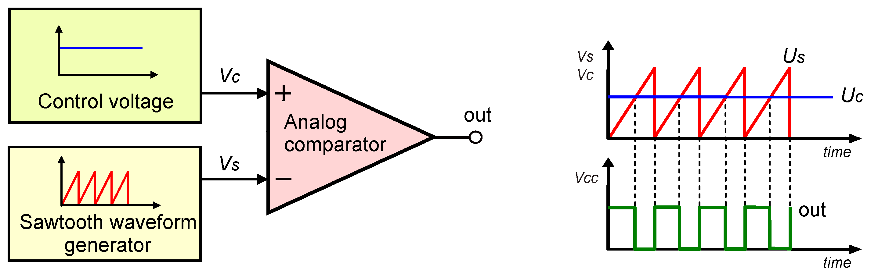
The most straightforward analog implementation of a PWM generator is presented in Figure 1, as a simplified block form. The voltage V s at the output of the sawtooth waveform generator increases linearly until it reaches its maximum value. When the sawtooth voltage equals the control voltage V c , the analog comparator changes the state of its output voltage. As a result, the generated PWM signal (whose pulse duty cycle depends on the relationship between the control voltage V c and the sawtooth waveform voltage V s ) has a frequency equal to the frequency of the generated sawtooth signal V s .
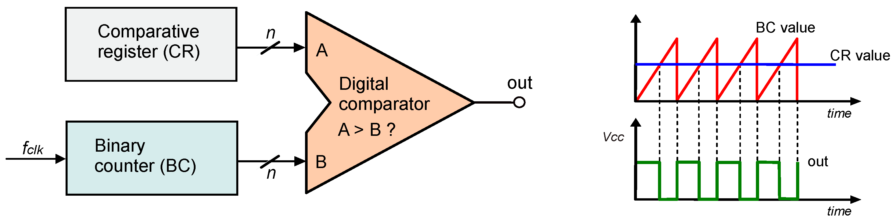
The same concept can be applied almost directly to digital circuits. An example counter-based solution of a digital PWM generator in the form of a simplified block diagram is shown in Figure 2.
The simplest form of the digital PWM generator consists of an n-bit binary counter BC that counts down or up and an n-bit comparative register CR, which stores information about the desired pulse width. If a down counter is used, it is loaded during overflow with a value corresponding to the period of the generated modulated signal. The CR register stores the digital value, representing the duty cycle of the generated pulses (Figure 2). The frequency of the clock signal f c l k (Figure 2) is 2 n times higher than the output frequency of the PWM signal (Equation (1)). In the case of high-resolution (large n value) and high-PWM signal frequency, the required clock signal frequency may be difficult to obtain. When the counter value is lower than the value of the CR register, the digital comparator output is set to the high logic level “1” but can easily be inverted.
f c l k = 2 n · f P W M ,
where n is the bit resolution of the PWM counter, defining the number of discrete steps ( 2 n ) per PWM period.
The PWM signal can be described as follows [27]:
x P W M ( t ) A , if 0 t mod T < D · T 0 , otherwise ,
where A is the amplitude of the PWM signal (in the following expressions it is assumed that A = 1 ), T is the signal period expressed in seconds [s], D [ 0 , 1 ] is the dimensionless duty cycle, and t R is the time. The notation ( t mod T ) expresses the cyclic nature of the signal that repeats every T seconds:
t mod T = t T t T .
The symbol · denotes the floor function, which returns the highest integer less than or equal to its argument. The PWM signal can also be represented as an infinite sum of rectangular functions shifted by the period T:
x P W M ( t ) = Π t n T D · T ,
where Π ( · ) denotes the rectangular function, defined as
Π ( t ) = 1 , if | t | < 1 2 0 , otherwise .
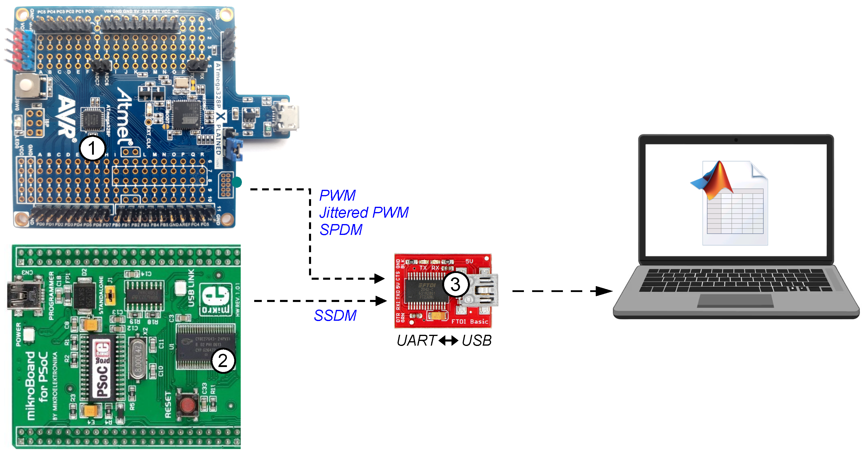
Digital control and PWM signals are a source of electromagnetic interference generation. The harmonics generated are particularly severe at low frequencies, which implies problems with output filter design. There is always a compromise between the price and size of the output filter (which influences the output signal quality) and, on the other hand, the dynamics of the output signals. SPDM (stochastic pulse-density modulation) or SSDM (stochastic signal density modulation) concepts can be considered an alternative. The idea is to spread the energy of the generated harmonics over a wider frequency band to make it easier to filter out these particularly undesirable harmonics due to their lower amplitudes. SPDM uses random (or pseudorandom) signal density modulation during the control period to generate a signal with a given average density. Figure 3 shows the basic components of a typical SPDM modulator. In this configuration, the maximum frequency of the generated SPDM waveform is equal to f c l k , which is the (random number generator) RNG clock frequency (Figure 3). For a practical use of this technique, PSoC systems (programmable system-on-chip) equipped with the necessary hardware blocks (e.g., random number generator) can be used [28]. Another viable option is to employ microcontrollers integrated with the appropriate hardware solutions.
The SPDM is a binary stochastic modulation technique. Each signal sample is independently determined according to a predefined probability [29,30,31]. This probability corresponds to the desired signal density. The SPDM signal x S P D M [ n ] is modeled as a Bernoulli random process according to the following formula:   
x S P D M [ n ] Bern ( p ) ,
where x S P D M [ n ] is the signal value in sample n, and p [ 0 , 1 ] is the modulation probability, representing the target average duty cycle (expected signal density). Physically, p defines the expected proportion of time the signal remains at a high logic level (“1”), which directly determines the mean output voltage and affects the spectral properties of the SPDM waveform. This implies P ( x S P D M [ n ] = 1 ) = p , and P ( x S P D M [ n ] = 0 ) = 1 p . For example, if p = 0.25 , then on average one out of every four samples will be equal to 1. Over time, the mean signal value will converge to 0.25, but high signal levels are randomly distributed. That feature distinguishes SPDM from SSDM, in which randomness is generated deterministically using an LFSR (linear feedback shift register) and compared with a reference value. SPDM is therefore a probabilistic modulation scheme. In the SPDM signal, the duty cycle for the n-th period depends on the number of pulses N n in that period, where N n is a random variable (for example, following a Bernoulli distribution). The formula for the duty cycle D n in the n-th period is given by the following:
D n = N n N max ,
where N n is the number of pulses in the n-th period, and N m a x is the maximum possible number of pulses that can fit into one period, based on the system clock. For a Bernoulli process, the expected duty cycle is as follows:
E [ D n ] = p ,
and the variance of the duty cycle is
Var ( D n ) = p ( 1 p ) .
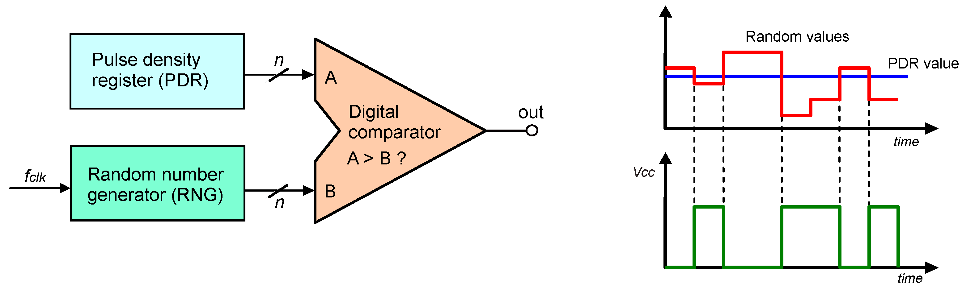
The presented SSDM generator does not use a binary counter in its structure. The generated waveform has a variable frequency and is not a PWM signal. Variable frequency control signals cannot be used in every power converter topology. In many power electronic converter topologies, especially in utilizing resonant circuits and soft switching of semiconductor power devices, changing the control frequency may cause unfavorable operating conditions for the power switches. That may severely degrade the conversion efficiency. However, random sequences can be used in systems controlled at a constant frequency with PWM signals, using solutions based on binary counters. In this type of configuration, no resonant circuits are used; therefore, the resonance period does not need to be maintained. The only limitation is the maximum frequency that can be used with acceptable switching losses. An example of a PWM generator that works with a randomly set duty cycle is shown in Figure 4. A constant frequency signal is obtained, and a random sequence controls the duty cycle. The RNG (random number generator) is clocked at f c l k / 2 n . This causes the PWM signal duty cycle to change every time the binary counter (BC) overflows. The current random value is compared to the BC binary counter. The stochastic modulated PWM signal is obtained from the output of the digital comparator (Figure 4).
The next presented idea of a modified PWM may be called a jittered PWM. In this case, the signal is a PWM waveform with duty factor intentionally subjected to controlled jitter [32,33,34]. Jitter in pulse-width modulation normally refers to unwanted variations in the timing of the PWM signal, essentially a deviation from the intended frequency and duty cycle. This can affect the accuracy of the PWM signal, leading to problems in applications such as motor control, audio generation, or data transmission. But in this case, if the jitter is properly controlled, the controlled output power may be properly set, the generated frequency spectrum is widespread, and the lower harmonics are attenuated.
Let the nominal period be T and the nominal high-time duration be τ . The jitter is modeled as a random variable Δ t n added to the falling edge timing in each PWM signal period n:
x P W M J i t t e r ( t ) = 1 , n T t < n T + τ + Δ t n 0 , n T + τ + Δ t n t < ( n + 1 ) T n Z ,
where T is the nominal period, τ is the nominal duration of the high state (pulse width), and Δ t n is the jitter applied to the falling edge timing in the n-th period and is a random variable with a bounded distribution typically satisfying Δ t n T . Due to falling edge jitter, the instantaneous duty cycle D n in each period n is slightly varied. The instantaneous duty cycle is defined as follows:
D n = τ + Δ t n T ,
Assuming that Δ t n is a random variable of zero mean ( E [ Δ t n ] = 0 ), the expected value and variance of the duty cycle are
E [ D n ] = τ T ,
Var ( D n ) = Var ( Δ t n ) T 2 .
This shows that jitter around the falling edge can be used to spread the spectrum of the PWM signal without changing its average energy.
The effect of jitter on the falling edge of the PWM signal can be modeled using different statistical distributions for the jitter value Δ t n . Two common distributions are the uniform and the Gaussian (bounded) distribution.
1.
Uniform distribution: The jitter Δ t n is uniformly distributed in the interval [ Δ t m a x , Δ t m a x ]:
Δ t n U ( Δ t m a x , Δ t m a x ) .
This means that the jitter has an equal probability of being any value within this range. The instantaneous duty cycle of the PWM signal is then affected by this jitter at each period n, with the falling edge of the signal shifted by a random amount within this interval.
2.
Gaussian distribution (bounded): The jitter Δ t n follows a Gaussian (normal) distribution with a mean of 0 and a standard deviation σ :
Δ t n N ( 0 , σ 2 ) , bounded by [ Δ t m a x , Δ t m a x ] .
However, to avoid excessive jitter, it is bounded within the interval [ Δ t m a x , Δ t m a x ]. This ensures that the jitter does not exceed a certain threshold. The Gaussian jitter typically causes smaller and more concentrated variations in the timing of the falling edge compared to the uniform distribution.
The uniform jitter distribution introduces an equal probability that the jitter is at any point within the defined range, causing noticeable random shifts in the falling edge timing of the PWM signal. The Gaussian jitter results in smaller and more concentrated variations around the mean, leading to subtler shifts in the duty factor.
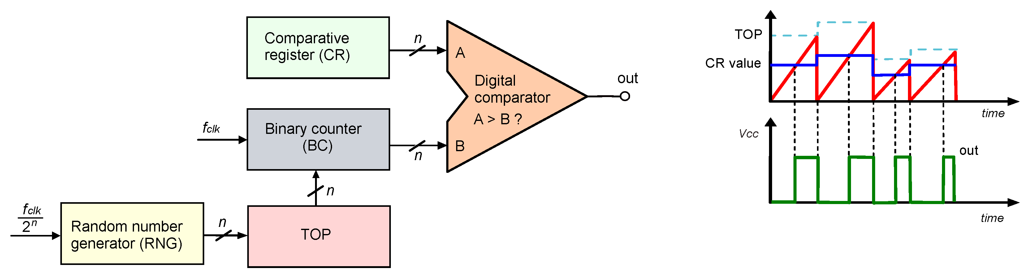
Figure 5 shows another topology of a PDM family, with a variable frequency output signal. This configuration uses a digital comparator to compare the set value of the CR comparative register with the state of the BC binary counter. The BC is clocked at the frequency f c l k and its capacity can be set by changing the TOP value (Figure 5). The TOP value is the maximum value of the binary counter. The counter counts from zero to the TOP value and then overflows and counts from zero again. Changing the top value affects the counter capacity and, as a result, the period of the generated PDM (pulse-density modulation) signal. In this configuration, the RNG random number generator, which is necessary to obtain the SPDM signal, is clocked at f c l k / 2 n . The binary counter is clocked at f c l k . The maximum output signal frequency that can appear in the SPDM output signal is also f c l k .
A similar effect can be achieved using the topology shown in Figure 6. In this case, the counter does not count from zero, but from the set BOTTOM value. Changing this value changes the period of the generated PDM signal. If the change in the BOTTOM value is controlled by a random sequence from the RNG generator, an SPDM signal is obtained at the digital comparator output. The RNG generator must be clocked at frequency f c l k / 2 n , while the BC counter is clocked at f c l k . As in the previous configurations, the counter capacity affects the resolution of the output signal control. The set value, stored in the OCR register, can be fixed or variable, depending on the application’s needs.

2.2. Stochastic Signal Density Modulation

Stochastic signal density modulation SSDM is a power modulation technique that can be viewed as a special case of pulse-density modulation (PDM) or random pulse-width modulation (RPWM). An example block diagram, which illustrates the principle of SSDM signal generation, is shown in Figure 7. Pseudorandom-width pulses adjust the output power level. Pulses are generated such that the average signal value reflects the predefined ratio of high to low states.
The RNG generates random numbers that modify the output frequency of the clock generator CG. The clock signal f g clocks with modulated frequency the binary counter BC. The comparative CR register stores the value to compare with the binary counter. The SSDM signal is achieved at the comparator output.
SSDM is a binary signal x S S D M [ n ] generated based on the comparison of a random sequence with a reference value [35,36]. This process modulates the signal density in a stochastic manner. The general form of x S S D M [ n ] is given by the following:
x S S D M [ n ] 1 , if r [ n ] < ρ 0 , otherwise ,
where x S S D M [ n ] is the signal value in sample n, ρ is the modulation density with ρ ( 0 , 1 ) , and r [ n ] is the random sequence.
In SSDM, the pulse density ρ refers to the average number of pulses per unit of time. The pulse density directly influences the duty cycle. For the period n-th, the duty cycle D n is defined as follows:
D n = N n T ,
where N n is the number of pulses in the n-th period, and T is the total time of a single period. The pulse density ρ is defined as the average number of pulses per time unit and can be written as follows:
D n = N a v g T ,
where N a v g is the average number of pulses per period T. Therefore, D n will be related to the specified pulse density ρ , and these parameters will be on average the same: D n ρ . The average duty cycle in SSDM with ρ will be equal to the given pulse density:
E [ D n ] = ρ .
The variance of the duty cycle D n depends on the statistical distribution of pulses over time. Assuming that the pulses follow a Poisson distribution (a common model for stochastic processes with a specified rate), the variance of the duty cycle is equal to the pulse density ρ . This can be expressed as follows:
Var ( D n ) = ρ .
Thus, the variance equals the specified signal density ρ when the pulses are randomly distributed according to a Poisson distribution.

2.3. Spectral and Statistical Analysis of Variable Pulse-Width Modulated Signals

In digital modulation techniques, the spectral characteristics of the output signal are crucially important, especially in power electronics and audio applications. The following forms are the most common for signal representation and analysis [37,38,39,40,41].
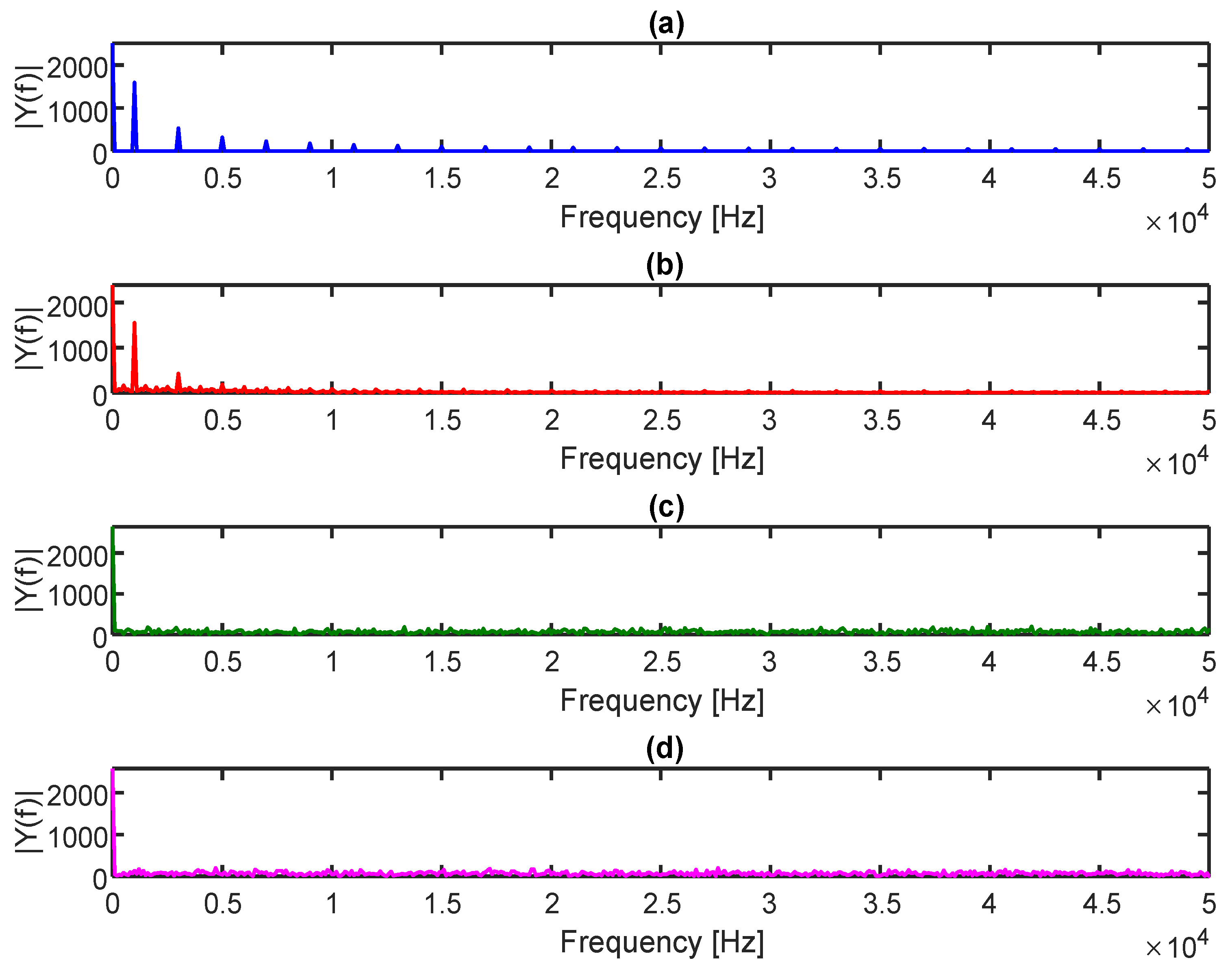
The discrete Fourier transform DFT is a fundamental tool for analyzing the frequency components present in a discrete-time signal. It allows identification of periodic content and harmonic structure in digital modulation schemes. The spectrum X [ k ] of a digital signal x [ n ] can be calculated using the following formula:
X [ k ] = n = 0 N 1 x [ n ] · e j 2 π k n N , k = 0 , 1 , , N 1 ,
where x [ n ] is the input signal in discrete time, X [ k ] is the Fourier transform coefficient in the frequency bin k, N is the number of samples, and j is the imaginary unit.
The power spectral density PSD describes how the power of a signal is distributed across different frequencies. It is useful for evaluating spectral spreading and harmonic suppression in modulated signals. The following expression provides an estimate of the discrete-time PSD:
PSD d ( f ) = 1 N f s n = 0 N 1 x [ n ] · e j 2 π f n f s 2 ,
where x [ n ] is the discrete-time signal, f s is the sampling frequency, and N is the number of samples used for the estimation.
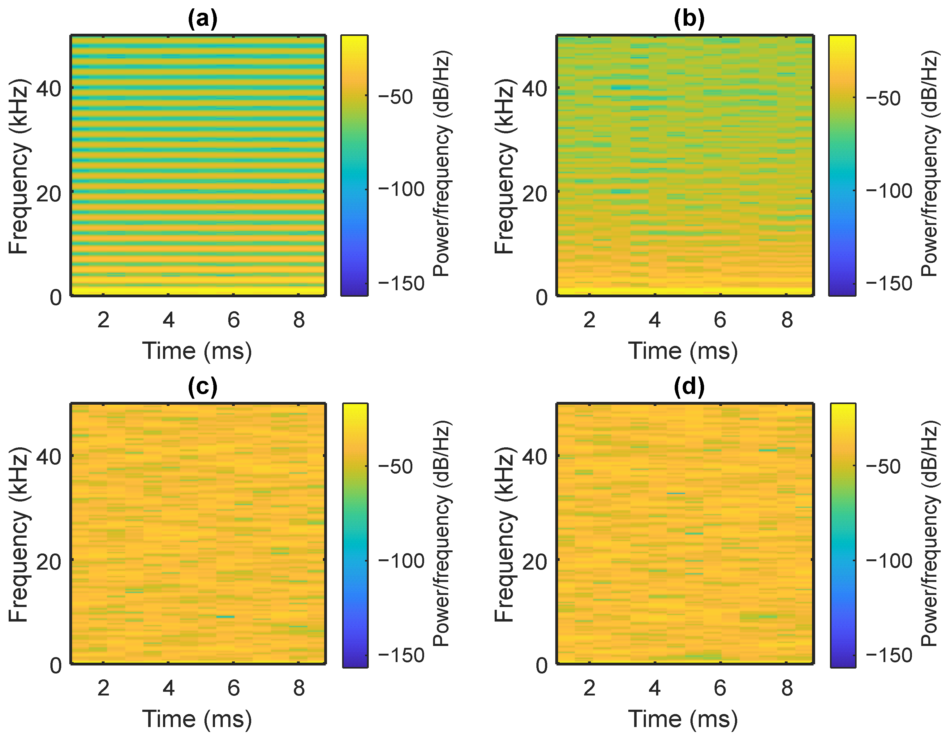
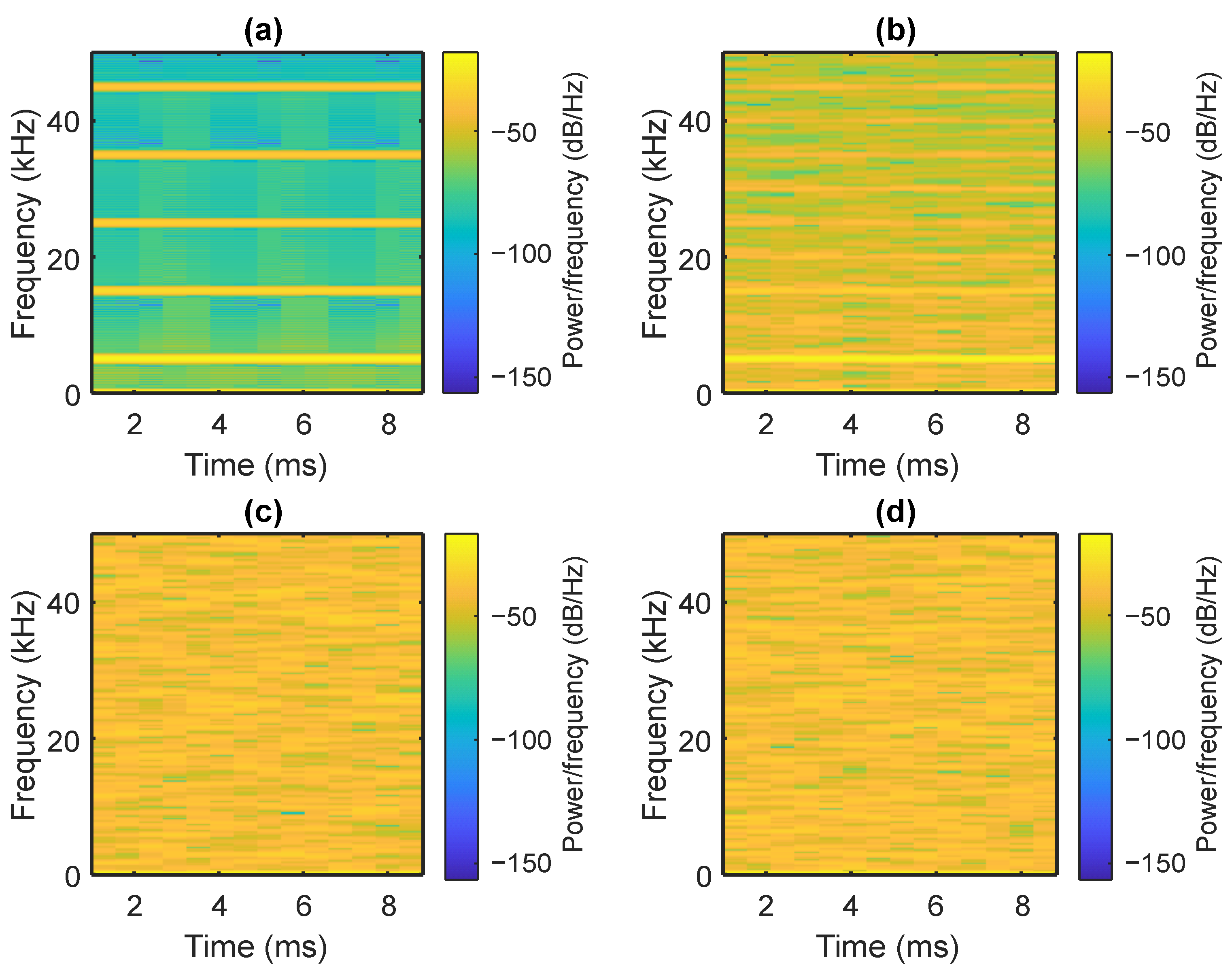
The spectrogram provides a time-varying view of the spectral content of a signal. It reveals how energy distribution across frequencies evolves, which is particularly useful for analyzing nonstationary or jittery signals. It is calculated as follows:
S ( t , f ) = n x [ n ] · w [ n t ] · e j 2 π f n 2 ,
where x [ n ] is the discrete-time signal, w [ n t ] is a window function (e.g., Hamming or Hann) centered at time t, f is the frequency, and j is the imaginary unit.
Autocorrelation quantifies the similarity between a signal and a delayed version of itself. It helps identify periodicities, signal predictability, and the degree of randomness in switching patterns. The discrete-time autocorrelation function is calculated as follows:
R x x [ τ ] = 1 N n = 0 N 1 τ x [ n ] · x [ n + τ ] ,
where τ is the delay in the samples and N is the number of samples.

3. Materials and Methods

This section presents software- and hardware-based approaches for generating selected signals, as described in Section 2. The hardware configuration employed in the experimental studies is based on chosen microcontrollers and is discussed in detail.

3.1. Software and Hardware Methods for Generating Variable Pulse-Width Signals

The generation of PWM signals in microcontrollers is accomplished using internal timers/counters, which are configured to count system clock pulses. Based on the values set in the comparative registers, the timer triggers a transition in the output’s logic state (from low to high or vice versa) at a specified time. The duration for which the output remains in the high or low state determines the duty cycle of the PWM signal. This duty cycle is proportional to the value in the comparative register relative to the total timer count, allowing precise control of the pulse width. Most microcontrollers are equipped with dedicated timer registers and modes, such as fast PWM, phase correct, or frequency and phase correct (in AVR microcontrollers), which automatically generate a PWM signal based on the preset parameters (frequency and duty cycle), without CPU intervention necessary. Although microcontrollers have built-in hardware blocks for generating PWM, it is also possible to implement it entirely in software. In this case, the user must manually manage the timing of the pulses using appropriate interrupts, loops, and clock management, which results in a higher CPU load and less precision. An example of such an implementation in pseudo-code form is shown in Listing 1.
Listing 1. The idea of software PWM signal generation.
Electronics 14 02651 i001
The variable d u t y _ c y c l e represents the percentage of the period when the output is in the high state, p e r i o d _ t i c k s is the total number of ticks that make up one full PWM period (high + low phases), and c o u n t e r tracks the progress within the current PWM period. It increments with each loop iteration. Conditional logic sets the output to high or low according to the counter. When the counter reaches p e r i o d _ t i c k s , it resets to 0, starting a new PWM cycle. The function w a i t _ f i x e d _ t i m e ( ) generates a small delay after each state change (high/low), corresponding to one tick, before rechecking the counter.
SPDM, SSDM, and jittered PWM signals are examples of modulations that can be generated both in software and hardware (SSDM only in microcontrollers of the PSoC1 family, while jittered PWM in most microcontrollers). However, in many microcontrollers, the generation of SPDM and SSDM signals implies a software implementation because of their stochastic nature, which requires flexible control over the pulse random durations or occurrences.
SPDM relies on random modification of pulse density: The number of pulses per unit time varies randomly, resulting in a variable duty cycle. Therefore, to successfully implement an SPDM, it is necessary to use appropriate algorithms in the code to ensure random pulse timing. Listing 2 presents the software implementation for generating this signal.
Listing 2. The idea of software SPDM signal generation.
Electronics 14 02651 i002
The variable p r o b a b i l i t y defines the target p (from 0 to 1). In the main loop, a random value between 0 and 1 is generated in each iteration using r a n d o m _ f l o a t _ 0 _ 1 ( ) . If the random value is smaller than the probability p, the output is set to high (1); otherwise, the output is set to low (0). After each iteration, w a i t _ f i x e d _ t i m e ( ) ensures a consistent sampling rate before the next iteration.
SSDM modulation is similar to SPDM but operates on more complex signals that account for both changes in pulse density and their random shifts in time. SSDM can be used to generate more complex random signals. Although SSDM must be implemented in software in most microcontrollers, some units, such as the PSoC1 family, offer hardware support for such modulation. This allows SSDM to be generated without overloading the processor. The implementation of SSDM in the software is shown in Listing 3.
Listing 3. The idea of software SSDM signal generation.
Electronics 14 02651 i003
The variable t h r e s h o l d defines the reference threshold value for comparison, m a x _ l f s r _ v a l u e is the maximum possible value for the LFSR, and l f s r _ s t a t e is the current state of the LFSR, initialized with the seed value. The LFSR state is updated by calling n e x t _ l f s r ( l f s r _ s t a t e ) in the main loop, which generates a new pseudo-random number. The output is set to high (“1”) if the LFSR state is lower than the threshold, or low (“0”) when the LFSR state is greater than or equal to the threshold. After each iteration, w a i t _ f i x e d _ t i m e ( ) ensures a consistent clock for periodic execution. The SPDM signal can be generated similarly to the SSDM using the LFSR register. In SSDM, the threshold dynamically follows a rapidly changing reference signal, allowing the output density to track high-frequency variations precisely. In contrast, SPDM uses a fixed or slowly varying threshold corresponding to a constant or slowly changing target probability. Although both techniques compare an LFSR-generated pseudorandom number with a threshold, SSDM is designed for accurate signal tracking, while SPDM is more suitable for maintaining a stable average output density over time. Quite structurally, their implementations are similar, but their applications and response dynamics differ significantly.
Jittered PWM is a type of PWM in which the moments of state change (switching between high and low) are randomly dispersed, thereby introducing variability in the pulse durations. In contrast to classical PWM, where the timing of state changes is deterministic, jittered PWM introduces random variations in the transition times. These random variations can be advantageous in applications that require non-uniform signals, such as the generation of random noise in digital systems. This modulation is typically implemented in software by introducing randomness into the pulse durations. A software-based implementation for generating a jittered PWM signal is presented in Listing 4. The variables m i n _ h i g h _ t i m e and m a x _ h i g h _ t i m e define the minimum and maximum allowed durations for the high state, while t o t a l _ p e r i o d represents the total period of PWM (sum of high and low phases). In the main loop, a high random time is generated within the specified bounds using r a n d o m _ b e t w e e n ( m i n _ h i g h _ t i m e , m a x _ h i g h _ t i m e ) . The corresponding low time is calculated to ensure that the total period remains constant. The output is then set to high for a random duration, followed by low for the remaining time. After each phase, the program waits for the respective duration.
Listing 4. The idea of software jittered PWM signal generation.
Electronics 14 02651 i004

3.2. Pseudo-Random Sequence Generation and SSDM Technique Available in PSoC1-Family Microcontrollers

As mentioned above, both standard PWM and jittered PWM signals can be generated on any microcontroller (8- or 32-bit) using dedicated internal peripheral modules. In contrast, the generation of pseudorandom modulated signals is typically not supported by hardware in most microcontrollers. An exception is the PSoC1 family of reconfigurable microcontrollers (originally developed by Cypress Semiconductor, now part of Infineon Technologies AG), which includes dedicated hardware resources for such functionality. This section discusses the relevant capabilities of the PSoC1 architecture.
A pseudo-random generator (PRG) is a deterministic function that, when initialized with a random input called a seed, produces an output sequence that appears random to any observer who does not know the seed. Despite their seemingly random behavior, PRGs are fully deterministic: given the same seed, they always produce the same output sequence. The fundamental difference between a PRG and a true random generator may be recognized by entropy, which quantifies the amount of uncertainty or information in the output. In the case of a PRG, the entropy of the generated sequence cannot exceed the entropy of the seed since the output is entirely determined by it. In contrast, a true random generator produces an output sequence in which each of the n bits contributes one bit of entropy, resulting in a total entropy of n. Consequently, such sequences are truly unpredictable.
PSoC1 microcontrollers offer a convenient means of generating pseudorandom sequences, enabled by their internal digital blocks. The blocks are designated PRSx (x = 8, 16, 24, 32) and can be configured freely. These blocks generate the desired length ( 2 x 1 ) sequence. The values obtained can then be used to modify the pulse width.
A simplified block diagram of the 8-bit PRS module is shown in Figure 8.
Figure 9 illustrates the occupancy of PRS digital blocks in the PSoC1 microcontroller, as a function of the desired length of the pseudorandom sequence.
In the generator considered, the combinational logic block is implemented as a network of XOR gates (see Figure 8). The LFSR (linear feedback shift register) acts as a pseudorandom sequence generator when configured to produce sequences of maximal length, which means that the circuit can cycle through 2 n 1 unique states, where n is the number of flip-flops in the SR shift register (see, e.g., [42,43,44,45]).
Each bit of the register is involved in an XOR operation, and the result is fed back into the most significant bit, while the remaining bits are shifted one position to the right. The least significant bit becomes the next output bit of the generated sequence. The LFSR must never be initialized with an all-zero state, as it would remain zero indefinitely due to the nature of the feedback mechanism. Therefore, the LFSR must be seeded with an initial non-zero value.
If the linear feedback shift register (LFSR) is initialized with a value of 1, its state after the first shift corresponds to the feedback polynomial mask. When initialized with only the most significant bit (MSB) set, the MSB propagates toward the least significant bit (LSB) position with each shift, and zeros are shifted into the vacated positions. The MSB is involved in the feedback calculation through XOR logic for all possible configurations.
The combinational feedback circuit is represented by a polynomial function of the general form [46]:
f ( x ) = k = 0 n a k x k ,
where x represents the unit delay introduced by a single flip-flop, x k denotes the delay to the output of the k-th flip-flop, and n denotes a number of bits in a digital hardware solution of LFSR. The coefficients a i take values of 0 or 1, depending on whether the output signal of the i-th flip-flop is included in the feedback path. In this configuration, a 0 = 1 . The resolution n of the LFSR is directly associated with the degree of the corresponding feedback polynomial. The polynomial can be software-defined as a hexadecimal number passed as an argument to an API function. A simple (primitive) polynomial, which ensures maximal-length sequences, generally takes the following form:
W s ( x ) = a n 1 x n 1 + . . . a 1 x + 1 .
The modular (reciprocal) polynomial associated with (25) has the following form:
W m ( x ) = x n + a 1 x n 1 + . . . + a n 1 x + 1 .
Given the available lengths of the pseudo-random sequence, the corresponding polynomials are of the following form [47,48]:
  • n = 8:
    W s ( x ) = x 8 + x 4 + x 3 + x 2 + 1 ( m a s k : 0 x 1 D )
    W m ( x ) = x 8 + x 6 + x 5 + x 4 + 1 ( m a s k : 0 x B 8 )
  • n = 16:
    W s ( x ) = x 16 + x 14 + x 13 + x 11 + 1 ( m a s k : 0 x 002 D )
    W m ( x ) = x 16 + x 5 + x 3 + x 2 + 1 ( m a s k : 0 x B 400 )
  • n = 24:
    W s ( x ) = x 24 + x 23 + x 22 + x 17 + 1 ( m a s k : 0 x E 10000 )
    W m ( x ) = x 24 + x 7 + x 2 + x 1 + 1 ( m a s k : 0 x 00 C 006 )
  • n = 32:
    W s ( x ) = x 32 + x 22 + x 2 + x 1 + 1 ( m a s k : 0 x C 00400006 )
    W m ( x ) = x 32 + x 31 + x 30 + x 10 + 1 ( m a s k : 0 x C 0000400 )
To effectively utilize the PRS block, it is necessary to define a simple (primitive) polynomial (25) that automatically determines the corresponding modular polynomial (26) based on the specified length n, using its reordered form (as shown in Equations (29), (31), (33) and (35)).
The PRS block (see Figure 8) operates as follows: the S R register implements the LFSR function, the P R register stores the primitive polynomial suitable for generating sequences of length n, and S R also serves to initialize the starting value. Before setting the start bit in the PRS control register, both the S R and P R registers must be properly initialized.
The SSDM technique in PSoC1 microcontrollers leverages dedicated, ready-to-use hardware blocks. Unlike other implementations (e.g., [49,50,51] and references therein), it is not necessary to implement individual components of SSDM circuitry either in software or as custom hardware logic. Instead, several predefined initialization API functions are available, significantly simplifying the configuration process. A schematic diagram of the internal structure of the configurable hardware SSDM module, available in the PSoC1 family, is shown in Figure 8. Due to the flexible and extensive clock generation system, the frequency of the output signal can be precisely adjusted by configuring the clock inputs to the relevant functional blocks.
The SSDM module shown in Figure 10, depending on the required signal resolution (density), can be constructed from either a single digital block (8-bit) or four digital blocks (32-bit) available in the microcontroller architecture. This flexibility is important and allows the user to balance the SSDM signal requirements with the limited number of digital resources (blocks) available for other purposes in the microcontroller. Figure 11 illustrates the allocation of the SSDM digital blocks, with a configuration analogous to that of the PRS blocks.
The stochastic counter S C (Figure 8) is responsible for generating pseudorandom numbers in the range from 1 to 2 n 1 with each tick of the signal f c l k . It is implemented as an LFSR register. The selection of resolution n will automatically determine the corresponding modular polynomial for the LFSR. The SDSD register holds the n-bit value that represents the signal density. This value is effectively within the range from 0 to 2 n 1 , which corresponds to a signal density between 0 and 100 % . In each cycle of the SSDM block, the stochastic counter value (LFSR shift register) is compared to the S D value. The module C M P operates in two modes, resulting in a change in logic states [28]:
1.
Mode 1 (less than or equal)—the output signal reaches a logical high state (“1”) when the value of S C is less than or equal to the desired signal density value;
2.
Mode 2 (less than)—the output signal reaches a logical high state (“1”) when the value of S C is less than the desired signal density value.
The signal density thus serves as the trip threshold for the CMP module. Once the SSDM module is initialized with the signal density value and the primitive polynomial, it is activated, and the rising edge of the clock signal generates the next counter state in the specified pseudorandom sequence. The following two parameters must be configured in the individual SSDM block:
  • Dimming Resolution ( P D R ) —can be in the range: 2…8 (8-bit), 2…16 (16-bit), 2…24 (24-bit), and 2…32 (32-bit). It sets the period of the stochastic counter to a value of ( 2 n 1 ) , where n is P D R ;
  • Signal Density ( P S D ) is a parameter that can take a value from 0 to ( 2 n 1 ) , whereby n = P D R (as above).

3.3. Experimental Setup

The variable pulse-width signal generation methods described in Section 2.1 and Section 2.2 have been achieved with the hardware configuration shown in Figure 12.
PWM and jittered PWM signals were generated using an Xplained Mini development board with an ATmega328P microcontroller (marked ➀) by configuring hardware timers. A software-based SPDM signal was implemented on the same microcontroller using a pseudorandom number generator. Furthermore, a microBoard platform with a CY8C27643 microcontroller (marked ➁) from the PSoC1 family was used to generate an SSDM signal based on hardware randomization. Each microcontroller (only one at a time) transmitted the sampled signal data via the UART interface (115200 baud, 8N1 configuration) to a laptop for analysis. The signal data from one microcontroller was transmitted and processed sequentially before moving on to the next signal generation task. This ensured that data from each microcontroller were analyzed independently, one at a time, before generating the next signal. Data received via UART were processed by a script, running in Matlab (version R2021b), designed for real-time acquisition. The script established a serial communication interface, continuously read incoming data streams, and stored the data in pre-allocated memory buffers to ensure processing efficiency. Upon reaching the pre-defined number of samples, the script automatically performed signal visualization in the time and frequency domains. In addition, a basic data validation routine was implemented to detect and discard incomplete or corrupted frames during transmission.
In all experiments (described in Section 4), the generated signals were binary-valued digital waveforms with amplitude levels of 0 V or 5 V (relative to the supply voltage of the microcontrollers), corresponding to the low and high states, respectively. Consequently, the average value of each signal μ x was considered in this range:
x [ n ] { 0 , A } , where A = 5 V .
To allow a fair comparison between the PWM, jittered PWM, SPDM, and SSDM signals, it was essential to ensure that all signals maintained the same long-term average value. This average corresponds directly to the intended signal density or duty cycle d [ 0 , 1 ] , scaled by the amplitude A. The target mean value is given by the following:
μ x = lim N 1 N n = 0 N 1 x [ n ] = d · A .
In practice, this was achieved by defining a reference value D ref = d · M , where M denotes the resolution of the modulation method (for example, maximum PWM counter, LFSR space, or number of quantization levels). Then, each modulation method used this threshold to compare against a ramp, counter, or random number to determine whether to generate a high or low output. This ensured that the probability of outputting a logical high, and hence the average value, matched the desired setting. The following equations define the output signal x [ n ] for each modulation scheme in terms of the reference value  D ref :
  • PWM (ATmega328P):
    x [ n ] = A , if mod ( n , N p ) < D ref 0 , otherwise where N p = f clk f P W M .
  • Jittered PWM (ATmega328P):
    x [ n ] = A , if mod ( n , N p ) < D ref + J [ n ] 0 , otherwise ,
    where
    J [ n ] [ J max , J max ] , J max = v · N p , v = 0.1 ( e . g . , ± 10 % jitter value ) .
  • SPDM (ATmega328P):
    x [ n ] = A , if rand ( 0 , M 1 ) < D ref 0 , otherwise ,
    where M is the number of quantization levels, determining the resolution of the probability space.
  • SSDM (PSoC1 – CY8C27643):
    x [ n ] = A , if LFSR [ n ] < D ref 0 , otherwise ,
    where LFSR [ n ] denotes the current value from a hardware linear-feedback shift register of resolution M = 2 k .
By adopting this unified thresholding approach, all modulation techniques produced signals with identical time-averaged voltage values (for example, μ x = 1.25 V for d = 0.25), enabling consistent and meaningful comparisons in terms of spectral content and time-domain behavior.
A clear overview of the implementation principles is provided in Table 1, which summarizes the core mechanisms, resolution M, for each modulation method used in the experiments. All techniques were configured to produce binary-valued output signals with an average value corresponding to the target duty cycle or signal density. In particular, the jittered PWM method extends classic PWM by introducing a random phase offset J [ n ] at each period, which modulates the switching instant within a defined jitter range (e.g., ± 10 % of the PWM period), thus adding temporal variability to the duty cycle transitions while maintaining the same average signal density.

4. Results

The information about generated harmonics is very important from designer and application points of view. Understanding the frequency spectrums of various pulse modulation techniques is crucial for effective signal processing and system design. Each modulation technique exhibits a unique frequency spectrum. By analyzing these spectra, we can design filters that target specific harmonic frequencies, ensuring efficient signal processing and compliance with regulatory standards. Understanding the frequency characteristics of modulation techniques allows an improvement of system performance for specific application needs.
This chapter discusses the modulation methods introduced in Section 2.3. We have tested the presented methods in various conditions. Sample frequencies from the range most often used in our case were selected for presenting in the article for the PWM and jittered PWM signals: 1 kHz and 5 kHz. The presentation of these two cases allows us to show how the operation changes when the frequency increases or decreases. For PWM, jittered PWM, SSDM, and SPDM, three target average output voltage levels were assumed for comparative analysis: 0.25%, 50%, and 75%. Given a signal amplitude of 5 V, these correspond to output voltages of 1.25 V, 2.5 V, and 3.75 V, respectively. The jitter was set to ± 20 % based on preliminary tests balancing spectral spreading and signal stability. Smaller jitter values yielded limited harmonic reduction, whereas larger values introduced timing instabilities. Although the average output level remained stable, the short-term irregularity of the pulses increased. In hardware PWM implementations, excessively large jitter amplitudes can also cause comparison of register overflows, preventing correct modulation and making ±20% an effective compromise. The SSDM signal was generated using a 32-bit solution and a polynomial (35). The performance of SSDM strongly depends on the length of the underlying LFSR sequence. Shorter LFSRs (8- or 16-bit) produce shorter, more repetitive sequences, leading to pronounced spectral harmonics and less effective noise shaping. In contrast, longer sequences generated by a 32-bit LFSR significantly improve harmonic suppression and spectral spreading by producing more noise-like modulation with reduced discrete spectral lines. This trade-off between sequence length and hardware complexity is fundamental in SSDM design.
Following the experiment, representative plots were selected for each signal type (Figure 13, Figure 14, Figure 15, Figure 16, Figure 17, Figure 18, Figure 19 and Figure 20), illustrating both spectral and temporal differences between the modulation techniques evaluated at an average voltage of 2.5 V. To ensure clarity of the results presented, key observations for the levels of 1.25 V and 3.75 V are summarized in Table 2 and Table 3.
As mentioned above, to avoid redundancy, Table 2 and Table 3 provide qualitative summaries of the spectral and time domain characteristics of the PWM, jittered PWM, SPDM, and SSDM signals for average values of 1.25 V and 3.75 V. The observed trends are consistent with those described in the detailed analysis for 2.5 V. The qualitative assessments summarized in the table apply to both the 1 kHz and 5 kHz base frequencies. Increasing the carrier frequency mainly shifts the spectral content toward higher frequencies but does not alter the modulation characteristics or their impact on the EMI behavior.
In the case of signals with a base frequency of 1 kHz and average voltage values of 1.25 V, 2.5 V, and 3.75 V, clear differences in the behavior of the individual modulation types were observed, among classic PWM, jittered PWM, SPDM and SSDM. Considering time-domain waveforms, the PWM signal is characterized by a regular periodic structure with fixed pulse widths. In the jittered PWM, this structure becomes smeared because of edge fluctuations. SPDM exhibits time variability in pulse widths resulting from the deterministic LFSR sequence, whereas SSDM displays a completely random binary noise-like nature while maintaining the target average value.
The amplitude spectrum (FFT) analysis shows that classic PWM produces strong, regular harmonics, particularly prominent at the 50% duty cycle, where even harmonics vanish and odd harmonics dominate. Jittered PWM causes partial blurring of these peaks, reducing their amplitudes. SPDM further disperses the spectral energy, though some local peaks remain, depending on the LFSR length. SSDM virtually eliminates all peaks in the spectrum; its profile closely resembles white noise.
The power spectral density (PSD) exhibits similar trends. PWM concentrates nearly all power in a few narrow frequency bands. Jittered PWM and SPDM broaden this distribution, while SSDM consistently has the lowest peak power values across the entire frequency band. The autocorrelation function of PWM reveals a strong temporal dependence: the impulses are fully predictable and structured. Jittered PWM weakens this regularity, but some correlation remains. SPDM shows a moderate decline in autocorrelation, while SSDM shows a complete loss of temporal structure, where the correlation drops immediately after lag zero.
Spectrograms reinforce these observations. In the case of PWM, stable horizontal energy bands are visible, indicating steady spectral content over time. In jittered PWM, these bands become irregular and dynamically distorted. SPDM spreads the energy more effectively, although certain localized frequency clusters remain. SSDM, in contrast, demonstrates full spectral diffusion over time and frequency, with no dominant regions, making it the most nonstationary signal among all tested.
When the base frequency is increased to 5 kHz, the qualitative behavior of the signals remains similar, although several quantitative changes appear in the spectral domain. In particular, dominant spectral components shift toward higher frequencies and the spacing between successive harmonics increases. This phenomenon facilitates analog filtering and reduces the risk of interference in lower frequency bands. PWM continues to generate strong harmonics, though they now span a broader spectral range. Jittered PWM and SPDM effectively reduce the peak amplitudes and flatten the spectrum. SSDM maintains its spectral flatness regardless of average value: the spectral profile remains evenly distributed and free of prominent components.
Autocorrelation patterns for 5 kHz confirm previous tendencies: deterministic signals like PWM remain highly correlated, jittered PWM and SPDM exhibit moderate loss of correlation, and SSDM consistently exhibits no correlation beyond lag zero. Spectrograms at this frequency also maintain similar interpretations: PWM produces static energy bands, jittered PWM and SPDM introduce spectral variability, and SSDM completely removes any stationary spectral features. The results suggest that higher base frequencies improve EMI performance by both dispersing energy and shifting it away from the critical frequency bands used by other systems.
Comparing all modulation signals tested at different average levels and two base frequencies leads to conclusive findings. Classic PWM demonstrates strong harmonic emissions, high time-domain correlation, and spectral energy concentration in narrow frequency bands. It is the least favorable technique from the viewpoint of electromagnetic compatibility. Introducing jitter significantly improves spectral properties: edge fluctuations efficiently reduce spectral peaks and distribute energy more broadly. SPDM, based on a deterministic but pseudo-random LFSR sequence, offers good spectral spreading and substantially reduces the risk of interference, especially with longer shift register lengths.
SSDM yields the best overall results. This technique, which compares the accumulated LFSR values against a reference threshold, is characterized by the highest entropy, complete lack of time-domain correlation, lowest-power spectral density, and fully nonstationary spectrograms. Its effectiveness becomes significant only when long-shift registers are used. Experimental evaluations were also performed for 8-bit and 16-bit SSDM implementations; however, these configurations showed insufficient performance and are not included in the results. A minimum of 24 bits is recommended for acceptable EMI behavior, and 32 bits are preferred to achieve consistent high-quality spectral diffusion.
This analysis confirms that jittered PWM, SPDM, and SSDM offer substantial improvements in spectral performance over classic PWM. If the objective is to achieve maximum EMI suppression and even energy dispersion across the frequency band, the 32-bit SSDM remains the most effective solution. In hardware constraint applications, jittered PWM or SPDM provides a practical and efficient alternative with a good balance of spectral performance and implementation simplicity.

5. Conclusions

This study presents a comprehensive evaluation of four pulse modulation techniques. PWM, jittered PWM, SPDM, and SSDM techniques are evaluated. The investigation included theoretical modeling, hardware/software implementation, and experimental verification using two microcontroller platforms: ATmega328P and CY8C27643. Signal analysis was performed in MATLAB, focusing on spectral properties and time-domain behavior. The results indicate that
  • PWM provides ease of implementation but produces harmonics at fixed frequencies that require filtering, which may be bulky or cost-prohibitive in compact designs.
  • Jittered PWM improves the EMI behavior by dispersing spectral energy via controlled variation of the switching instant. However, an improper jitter amplitude may result in an overflow of comparator registers (e.g., OCRx in AVR), leading to invalid PWM behavior.
  • SPDM, implemented in software using pseudorandom number generators, provides improved spectral uniformity but requires careful tuning of randomness sources and thresholds.
  • SSDM, using hardware-implemented LFSRs in the PSoC1 platform, delivers the most effective harmonic suppression and is well suited for systems where EMI compliance is critical.
The results and discussion confirm the novelty and practical relevance of this study, demonstrated by the unique hardware implementation of SSDM on the PSoC1 platform and the broad comparative analysis of multiple modulation techniques. These contributions provide valuable guidance for engineers and researchers seeking efficient harmonic suppression methods in embedded systems.
Future development directions may include hybrid modulation schemes that dynamically switch between deterministic and stochastic techniques based on operating conditions or EMI feedback; automated jitter adaptation algorithms to ensure safe operation within comparator register limits while maximizing spectral spreading; deployment of advanced microcontrollers or FPGAs featuring integrated high-resolution PWM generators and true or high-quality pseudorandom number generators.

Implementation Notes

Each modulation technique presents implementation-specific constraints, particularly in microcontroller-based systems with limited register width and timer resolution.
To ensure consistent output voltage averaged over time in all methods, a reference threshold D ref = d · M was used, where d denotes the desired duty cycle or signal density and M defines the modulation resolution.
In the case of PWM and jittered PWM, implemented on the ATmega328P, the resolution M is determined by the number of clock cycles per PWM period ( N p = f clk / f PWM ). For jittered PWM, the switching threshold varies around D ref by a random value J [ n ] [ J max , J max ] , where excessive jitter may exceed the valid range of OCR registers.
SPDM compares a random integer drawn uniformly from [ 0 , M 1 ] with D ref to determine the pulse output. The effectiveness of this method depends on the statistical quality of the random number generator (RNG) and the resolution of M.
SSDM, performed on PSoC1 using a hardware LFSR of resolution k ( M = 2 k ), compares each LFSR state with D ref . Provides superior statistical stability and spectral spreading, especially for 24- and 32-bit configurations. The use of dedicated hardware blocks minimizes CPU overhead and enables precise control of signal density and resolution.
All signals were normalized to the 0–5 V range, with long-term average values corresponding to the target output levels (1.25 V, 2.5 V, and 3.75 V, for duty cycles 25%, 50%, and 75%). Data consistency across modulation types was ensured by unified threshold logic.
Overall, the implementation results confirm the practical viability of stochastic and jittered modulation techniques and provide guidance for selecting suitable methods depending on the available hardware resources and EMI requirements.

Author Contributions

Conceptualization, W.W.; methodology, W.W. and R.K.; software, R.K. and W.W.; validation, R.K. and W.W.; investigation, R.K. and W.W.; data curation, R.K.; writing—original draft preparation, R.K. and W.W.; writing—review and editing, R.K. and W.W.; visualization, R.K. and W.W. All authors have read and agreed to the published version of the manuscript.

Funding

This research was funded by Bialystok University of Technology grant number WZ/WE-IA/5/2023.

Institutional Review Board Statement

Not applicable.

Informed Consent Statement

Not applicable.

Data Availability Statement

Dataset is available on request from the authors.

Conflicts of Interest

The authors declare no conflicts of interest.

References

  1. Holmes, D.G.; Lipo, T.A. Pulse width Modulation for Power Converters: Principles and Practice; John Wiley & Sons: Hoboken, NJ, USA, 2003; Volume 18. [Google Scholar]
  2. Calderon-Lopez, G.; Villarruel, A.; Kakosimos, P.; Ki, S.K.; Todd, R.; Forsyth, A. A Comparison of Digital PWM Control Strategies for High Power Interleaved DC-DC Converters. IET Power Electron. 2017, 11, 391–398. [Google Scholar] [CrossRef]
  3. Bushra, E.; Zeb, K.; Ahmad, I.; Khalid, M. A comprehensive review on recent trends and future prospects of PWM techniques for harmonic suppression in renewable energies based power converters. Results Eng. 2024, 22, 102213. [Google Scholar] [CrossRef]
  4. Liu, F.; Ruan, X.; Yao, K.; Gu, L.; Yang, F.; Tse, C.K. Full-Range Non-Resonant PWM Zero-Voltage-Switching Power Converters With Minimized Inductor Current Ripple. IEEE J. Emerg. Sel. Top. Power Electron. 2025, 13, 2014–2026. [Google Scholar] [CrossRef]
  5. Jing, T.; Maklakov, A.; Radionov, A.; Gasiyarov, V.; Liang, Y. Formulations, solving algorithms, existing problems and future challenges of pre-programmed PWM techniques for high-power AFE converters: A comprehensive review. Energies 2022, 15, 1696. [Google Scholar]
  6. Mohammed, S.A.Q.; Jung, J.W. A state-of-the-art review on soft-switching techniques for DC–DC, DC–AC, AC–DC, and AC–AC power converters. IEEE Trans. Ind. Inform. 2021, 17, 6569–6582. [Google Scholar] [CrossRef]
  7. Kim, J.W.; Barbosa, P. PWM-controlled series resonant converter for universal electric vehicle charger. IEEE Trans. Power Electron. 2021, 36, 13578–13588. [Google Scholar] [CrossRef]
  8. Tomoyasu, H.; Omori, H.; Mishima, T. Constant Frequency Edge-Resonant ZVS-PWM High-Frequency Inverter for Domestic Induction Heating Cooktops. In Proceedings of the 2023 IEEE Energy Conversion Congress and Exposition (ECCE), Nashville, TN, USA, 29 October–2 November 2023; pp. 2318–2325. [Google Scholar]
  9. Alatai, S.; Salem, M.; Ishak, D.; Das, H.S.; Alhuyi Nazari, M.; Bughneda, A.; Kamarol, M. A review on state-of-the-art power converters: Bidirectional, resonant, multilevel converters and their derivatives. Appl. Sci. 2021, 11, 10172. [Google Scholar] [CrossRef]
  10. Al-Safi, A.; Al-Khayyat, A.; Manati, A.M.; Alhafadhi, L. Advances in fpga based pwm generation for power electronics applications: Literature review. In Proceedings of the 2020 11th IEEE Annual Information Technology, Electronics and Mobile Communication Conference (IEMCON), Vancouver, BC, Canada, 4–7 November 2020; pp. 252–259. [Google Scholar]
  11. Koutroulis, E.; Dollas, A.; Kalaitzakis, K. High-frequency pulse width modulation implementation using FPGA and CPLD ICs. J. Syst. Archit. 2006, 52, 332–344. [Google Scholar] [CrossRef]
  12. Syed, A.; Ahmed, E.; Maksimovic, D.; Alarcon, E. Digital pulse width modulator architectures. In Proceedings of the 2004 IEEE 35th Annual Power Electronics Specialists Conference (IEEE Cat. No. 04CH37551), Aachen, Germany, 20–25 June 2004; Volume 6, pp. 4689–4695. [Google Scholar]
  13. Morales-Leal, T.; Moreno-Munoz, A.; Ortiz-Lopez, M.A.; Geninatti, S.R.; Quiles-Latorre, F.J. New random PWM method at constant switching frequency and maximum harmonic reduction created with a flexible FPGA-based test bench. IEEE Access 2023, 11, 19385–19394. [Google Scholar] [CrossRef]
  14. Wojtkowski, W. Digital control of a bidirectional DC/DC converter for automotive applications. IFAC-PapersOnLine 2018, 51, 113–118. [Google Scholar] [CrossRef]
  15. Wojtkowski, W. Implementation of AVR hardware PWM blocks for power LED light intensity regulation. Prz. Elektrotechniczny 2009, 85, 306–309. [Google Scholar]
  16. Khalid, M.; Mohan, A.; Binojkumar, A.C. Carrier-Based Variable Frequency PWM Technique for PMSM Drives to Achieve Dispersed Spectrum and Extended Low-Speed Operation Capability. Arab. J. Sci. Eng. 2023, 48, 15045–15061. [Google Scholar] [CrossRef]
  17. Zhang, S.; Wang, X.; Zhou, K.; Shao, X.; Liu, J. Chaotic ant colony algorithm-based frequency-optimized random switching frequency SVPWM control strategy. J. Power Electron. 2023, 23, 1688–1702. [Google Scholar] [CrossRef]
  18. Reddy, M.H.V.; Reddy, T.B.; Reddy, B.R.; Kalavathi, M.S. Random PWM technique for dual-inverter-fed vector-controlled induction motor drive. J. Control Autom. Electr. Syst. 2016, 27, 60–68. [Google Scholar] [CrossRef]
  19. Xu, D.; Zhao, C.; Fan, H. A PWM plus phase-shift control bidirectional DC-DC converter. IEEE Trans. Power Electron. 2004, 19, 666–675. [Google Scholar] [CrossRef]
  20. Xiao, H.; Xie, S. A ZVS bidirectional DC–DC converter with phase-shift plus PWM control scheme. IEEE Trans. Power Electron. 2008, 23, 813–823. [Google Scholar] [CrossRef]
  21. Lee, I.O.; Moon, G.W. Phase-shifted PWM converter with a wide ZVS range and reduced circulating current. IEEE Trans. Power Electron. 2012, 28, 908–919. [Google Scholar] [CrossRef]
  22. Wojtkowski, W.; Karpiuk, A. The Influence of the PWM frequency and duty cycle of a RGB LED driver on the optical spectrum of the emitted light. Prz. Elektrotechniczny 2012, 88, 217–219. [Google Scholar]
  23. Mihali, F.; Kos, D. Reduced conductive EMI in switched-mode DC–DC power converters without EMI filters: PWM versus randomized PWM. IEEE Trans. Power Electron. 2006, 21, 1783–1794. [Google Scholar] [CrossRef]
  24. Alargt, F.S.; Ashur, A.S.; Kharaz, A.H. Performance comparison between PWM and SSDM techniques in interleaved boost converter. In Proceedings of the 2015 50th International Universities Power Engineering Conference (UPEC), Stoke on Trent, UK, 1–4 September 2015; pp. 1–7. [Google Scholar]
  25. Perumandla, S.; Upadhyay, P.; Jayalaxmi, A.; Nasam, J.P. Modulated Frequency Triangular Carrier Based Space Vector PWM Technique for Spreading Induction Motor Acoustic Noise Spectrum. In Proceedings of the International Conference on E-Business and Telecommunications, Prague, Czech Republic, 26–28 July 2019. [Google Scholar]
  26. Sadanandam, P.; Upadhyay, P.; Jayalaxmi, A. Modulated Frequency Triangular Carrier Based Discontinuous PWM Technique for Inverter Fed Induction Motor Drive. In Proceedings of the 2022 22nd National Power Systems Conference (NPSC), New Delhi, India, 17–19 December 2022; pp. 160–165. [Google Scholar]
  27. Rashid, M.H. Pulse Width Modulation—A Comprehensive Review. IEEE Trans. Ind. Electron. 2013, 60, 1232–1244. [Google Scholar]
  28. Cypress Semiconductor Corporation. Stochastic Signal Density Modulation Datasheet SSDM V 1.0; Ver.1.0; Cypress: San Jose, CA, USA, 2014. [Google Scholar]
  29. Sapatnekar, S.S.; Pjevalica, N. Stochastic signal processing using delta-sigma modulation. IEEE Trans. Circuits Syst. I Regul. Pap. 2002, 49, 345–356. [Google Scholar]
  30. Karam, L.J.; Prata, A.A. Stochastic Pulse Density Modulation for Signal Conversion and Noise Shaping. IEEE Trans. Circuits Syst. I Regul. Pap. 2006, 53, 1505–1516. [Google Scholar]
  31. Haykin, S. Communication Systems; John Wiley & Sons: Hoboken, NJ, USA, 2008. [Google Scholar]
  32. Lee, T.H. The Design of CMOS Radio-Frequency Integrated Circuits; Cambridge University Press: Cambridge, UK, 2004. [Google Scholar]
  33. Long, B.; Chen, W.; Hu, Z.; Bai, Y.; Liu, D.; Liu, H. An all-digital RF transmitter architecture based on jitter-enhanced PWM. Sci. Rep. 2025, 15, 9433. [Google Scholar] [CrossRef]
  34. McNeill, J.; Rincon-Mora, G.A. Noise Analysis of Jittered PWM Signals. IEEE Trans. Circuits Syst. II Express Briefs 2009, 56, 925–929. [Google Scholar]
  35. Nakano, K.; Haruyama, S. Stochastic Signal Density Modulation Using LFSR for Noise-Shaping. IEEE Trans. Circuits Syst. I Regul. Pap. 2015, 62, 1872–1880. [Google Scholar]
  36. Smith, S.W. Digital Signal Processing: A Practical Guide for Engineers and Scientists; Newnes: Burlington, MA, USA, 2003. [Google Scholar]
  37. Oppenheim, A.V.; Willsky, A.S.; Nawab, S.H. Signals & Systems; Pearson Educación: London, UK, 1997. [Google Scholar]
  38. Proakis, J.G. Digital Signal Processing: Principles Algorithms and Applications; Pearson Education India: Noida, India, 2001. [Google Scholar]
  39. Lyons, R.G. Understanding Digital Signal Processing, 3/E; Pearson Education India: Noida, India, 1997. [Google Scholar]
  40. MacKay, D.J. Information Theory, Inference and Learning Algorithms; Cambridge University Press: Cambridge, UK, 2003. [Google Scholar]
  41. Liu, L.; Miao, S.; Cheng, M.; Gao, X. Permutation entropy for random binary sequences. Entropy 2015, 17, 8207–8216. [Google Scholar] [CrossRef]
  42. Travis, B.; Swager, A. D/A-converter ASIC uses stochastic logic. EDN 1996, 41, 86–87. [Google Scholar]
  43. Goresky, M.; Klapper, A. Algebraic Shift Register Sequences; Cambridge University Press: Cambridge, UK, 2012. [Google Scholar]
  44. Grymel, M. New Programmable LFSR Counters with Automatic Encoding and State Extension. Electronics 2024, 13, 405. [Google Scholar] [CrossRef]
  45. Van Tilborg, H.C.; Jajodia, S. Encyclopedia of Cryptography and Security; Springer Science & Business Media: Cham, Switzerland, 2014. [Google Scholar]
  46. Groote, J.F.; Morel, R.; Schmaltz, J.; Watkins, A. Logic Gates, Circuits, Processors, Compilers and Computers; Springer: Cham, Switzerland, 2021. [Google Scholar]
  47. Cusick, T.W.; Ding, C.; Renvall, A.R. Stream Ciphers and Number Theory; Elsevier: Amsterdam, The Netherlands, 2004; Volume 66. [Google Scholar]
  48. Lin, S.; Costello, D.J. Error Control Coding; Prentice-Hall: Englewood Cliffs, NJ, USA, 2001; Volume 2. [Google Scholar]
  49. Akgul, A.; Li, C.; Pehlivan, I. Amplitude control analysis of a four-wing chaotic attractor, its electronic circuit designs and microcontroller-based random number generator. J. Circuits Syst. Comput. 2017, 26, 1750190. [Google Scholar] [CrossRef]
  50. Çiçek, S. Microcontroller-based random number generator implementation by using discrete chaotic maps. Sak. Univ. J. Sci. 2020, 24, 832–844. [Google Scholar] [CrossRef]
  51. Souaki, G.; Halim, K. Random number generation based on MCU sources for IoT application. In Proceedings of the 2017 International Conference on Advanced Technologies for Signal and Image Processing (ATSIP), Fez, Morocco, 22–24 May 2017; pp. 1–6. [Google Scholar]
Figure 1. Simplified block diagram of an analog PWM signal generator.
Electronics 14 02651 g001
Figure 2. Simplified block diagram of a digital PWM generator based on a binary counter. The variable n denotes the width of an n-bit data bus.
Electronics 14 02651 g002
Figure 3. Simplified block diagram of a digital SSDM/SPDM generator based on a random number generator. The variable n denotes the width of an n-bit data bus.
Electronics 14 02651 g003
Figure 4. An example of a PWM generator working with a randomly set duty cycle. The variable n denotes the width of an n-bit data bus.
Electronics 14 02651 g004
Figure 5. An example of a PDM generator, generating a signal with a variable frequency of the output pulses, with regulated TOP value. The variable n denotes the width of an n-bit data bus.
Electronics 14 02651 g005
Figure 6. An example of a PDM generator, generating a signal with a variable frequency of the output pulses, with regulated BOTTOM value. The variable n denotes the width of an n-bit data bus.
Electronics 14 02651 g006
Figure 7. Simplified block diagram of a digital SSDM generator based on a random number generator. The variable n denotes the width of an n-bit data bus.
Electronics 14 02651 g007
Figure 8. Block diagram of the PRS8 module available on the PSoC1 microcontroller (section shown in the gray background shows the internal configuration of the microcontroller in the PSoC Designer tool software).
Electronics 14 02651 g008
Figure 9. Availability of PRS blocks depending on sequence length: (a) 8-bit, (b) 16-bit, (c) 24-bit, (d) 32-bit.
Electronics 14 02651 g009
Figure 10. Block diagram of the 8-bit SSDM module available on the PSoC1 microcontroller (section shown in the gray background shows the internal configuration of the microcontroller in the PSoC Designer tool software). The variable n denotes the width of an n-bit data bus.
Electronics 14 02651 g010
Figure 11. Availability of SSDM blocks depending on resolution: (a) 8-bit, (b) 16-bit, (c) 24-bit, (d) 32-bit.
Electronics 14 02651 g011
Figure 12. Hardware configuration for processing and analysis of generated signals: 1—AVR microcontroller ATmega328P, 2—PSoC1 microcontroller CY8C27643, 3—UART/USB converter.
Electronics 14 02651 g012
Figure 13. Time-domain waveforms of (a) PWM, (b) jittered PWM, (c) SSDM, (d) SPDM, and average value 2.5 V (marked with red line). The frequency of signals (a,b) is 1 kHz.
Electronics 14 02651 g013
Figure 14. Amplitude spectra (FFT) of (a) PWM, (b) jittered PWM, (c) SSDM, (d) SPDM, and average value 2.5 V. The frequency of signals (a,b) is 1 kHz.
Electronics 14 02651 g014
Figure 15. Amplitude spectra (FFT) of (a) PWM, (b) jittered PWM, (c) SSDM, (d) SPDM, and average value 2.5 V. The frequency of signals (a,b) is 5 kHz.
Electronics 14 02651 g015
Figure 16. Power spectral density (PSD) of (a) PWM, (b) jittered PWM, (c) SSDM, (d) SPDM, and average value 2.5 V. The frequency of signals (a,b) is 1 kHz.
Electronics 14 02651 g016
Figure 17. Power spectral density (PSD) of (a) PWM, (b) jittered PWM, (c) SSDM, (d) SPDM, and average value 2.5 V. The frequency of signals (a,b) is 5 kHz.
Electronics 14 02651 g017
Figure 18. Autocorrelation function of (a) PWM, (b) jittered PWM, (c) SSDM, (d) SPDM, and average value 2.5 V. The frequency of signals (a,b) is 5 kHz.
Electronics 14 02651 g018
Figure 19. Spectogram of (a) PWM, (b) jittered PWM, (c) SSDM, (d) SPDM, and average value 2.5 V. The frequency of signals (a,b) is 1 kHz.
Electronics 14 02651 g019
Figure 20. Spectogram of (a) PWM, (b) jittered PWM, (c) SSDM, (d) SPDM, and average value 2.5 V. The frequency of signals (a,b) is 5 kHz.
Electronics 14 02651 g020
Table 1. Comparison of modulation methods used in the experiments.
MethodModulation PrincipleReference Threshold D ref Resolution M
PWMCompare counter with D ref d · M M = N p , number of clock cycles per PWM period
Jittered PWMPWM with randomized timing of the falling edge, modulated around nominal duty cycle by jitter percentage d · M Same as PWM
SPDMCompare random integer in [ 0 , M 1 ] with D ref d · M M defines quantization granularity (e.g., 256)
SSDMCompare LFSR output with D ref d · M M = 2 k , size of LFSR space
Table 2. Qualitative assessment of modulation signals for an average output value of 1.25 V.
SignalFFTPSDAutocorrelationSpectrogram
PWMStrong peaksMaximum powerHigh periodicityStationary frequency bands
Jittered PWMSmeared spectral linesLower peak levelsPartial decorrelationFluctuating frequency bands
SPDMSpread spectrumLow peak powerModerate decay of correlationIrregular energy distribution
SSDMNo dominant peaksMinimum powerNo correlationFully diffused over time and frequency
Table 3. Qualitative assessment of modulation signals for an average output value of 3.75 V.
SignalFFTPSDAutocorrelationSpectrogram
PWMStrong peaksHigh powerStrong correlationStable, repetitive bands
Jittered PWMBroadened peaksReduced power levelsLower correlationTime-varying band structure
SPDMUniformly distributed energyMedium-low PSDFast decorrelationFragmented spectrogram
SSDMFlat spectrumVery low powerNo correlationFully randomized frequency content
Disclaimer/Publisher’s Note: The statements, opinions and data contained in all publications are solely those of the individual author(s) and contributor(s) and not of MDPI and/or the editor(s). MDPI and/or the editor(s) disclaim responsibility for any injury to people or property resulting from any ideas, methods, instructions or products referred to in the content.

