Article

The Design and Performance Evaluation of a Compact, Low-Cost Rectenna on a 3D-Printed Composite Substrate for Sustainable IoT Devices

by
Blagovest Atanasov
,
Nikolay Atanasov
* and
Gabriela Atanasova
Department of Communication and Computer Engineering, South-West University “Neofit Rilski”, 2700 Blagoevgrad, Bulgaria
*
Author to whom correspondence should be addressed.
Electronics 2025, 14(13), 2625; https://doi.org/10.3390/electronics14132625 (registering DOI)
Submission received: 22 May 2025 / Revised: 24 June 2025 / Accepted: 27 June 2025 / Published: 29 June 2025

Abstract

The Internet of Things (IoT) is one of the pivotal technologies driving the digital transformation of industry, business, and personal life. Along with new opportunities, the exponential growth of IoT devices also brings environmental challenges, driven by the increasing accumulation of e-waste. This paper introduces a novel, compact, cubic-shaped rectenna with a 3D-printed composite substrate featuring five identical patches. The design aims to integrate RF energy harvesting technology with eco-friendly materials, enabling its application in powering next-generation sustainable IoT systems. Due to its symmetrical design, each patch antenna achieves a bandwidth of 130 MHz within the frequency range of 2.4 GHz to 2.57 GHz, with a maximum efficiency of 60.5% and an excellent isolation of below −25 dB between adjacent patch antennas. Furthermore, measurements of the rectifier circuit indicate a maximum conversion efficiency of 33%, which is comparable to that of other rectennas made on 3D-printed substrates. The proposed visually unobtrusive design not only enhances compactness but also allows the proposed rectenna to harvest RF energy from nearly all directions.

1. Introduction

The Internet of Things (IoT) is one of the pivotal technologies for the digital transformation of industry, business, and personal life, enabling the integration of physical devices, data, computational resources, and network connectivity [1,2]. Due to the wide range of applications, from wearables [3,4] to smart buildings [5], autonomous vehicles [6], precision agriculture [7], and industrial automation [8], an unprecedented increase in IoT devices is observed. The forecasts indicate that the IoT devices worldwide will surpass 32 billion by 2030 [9,10]. The growing number of IoT devices not only unlocks vast potential for enabling ‘smarter’ and more efficient functioning of the world around us but also will lead to a significant increase in electronic waste (e-waste) [11] and the need for more energy to power the massive number of smart devices [12,13]. Therefore, to reduce environmental impact and build a more responsible and ‘green’ IoT ecosystem, there is an increasing need to develop next-generation sustainable IoT devices that integrate eco-friendly materials and energy harvesting technologies at the early stages of their design and development [12,13,14,15].
In recent years, radio frequency energy harvesting (RF-EH) and wireless power transmission (WPT) have attracted significant attention as promising technologies to reduce the reliance on batteries of IoT devices, improving their sustainability [16,17,18,19,20,21]. The rectenna, consisting of an antenna and a rectifier, is considered the most essential component for the performance of a system for RF-EH and WPT [18,19,21,22,23,24].
A variety of antenna topologies for RF-EH have been presented, including patch [17,20,21,25], slot [19], monopole [22,23], spiral [24], and dipole [26] antennas. Also, various rectifier circuit architectures for RF-EH have been proposed and realized, including the half-wave rectifier [20,25,27], voltage doubling rectifier [19,22,24,26], and multilevel rectifier [17,23], such as Cockcroft–Walton and Villard. Moreover, many of the proposed rectenna designs incorporate non-degradable and non-recyclable materials for their elements, raising environmental concerns and limiting design flexibility. For instance, most antennas [17,19,20,22,24,26] have been designed and fabricated on commercially available substrates, such as FR4, Rogers 5880, and Rogers RT6010.
Organic [11,28] and biodegradable [29,30,31] materials have been identified as suitable for antenna substrates, enabling the implementation of eco-friendly materials in the early stage of the antenna design process. The most commonly used biodegradable material is polylactic acid (PLA). Additive manufacturing, also known as three-dimensional (3D) printing, is typically employed for shaping antennas with such material, as 3D printing offers numerous advantages, including reduced production costs and time, design flexibility, and the ability to produce complex and unique geometries, reducing material waste [21,23,29,30,31].
This article presents the design methodology and performance evaluation of a compact, low-cost rectenna fabricated on a 3D-printed composite substrate. The design integrates RF energy harvesting technology with eco-friendly materials, enabling its application in powering next-generation sustainable IoT systems.

2. Materials and Methods

2.1. Materials

We mainly used biodegradable and recyclable materials to fabricate the rectenna components. Among the wide range of materials available for 3D printing, we chose two materials for the fabrication of the 3D-printed composite substrate: a cost-effective, biodegradable PLA filament with a diameter of 1.75 mm (Jet Black, Prusa, Czech Republic) and a high-resolution polymer resin (Aqua-Gray 4K, Phrozen, Taiwan). We used brass foil, an easily recyclable material [32], to fabricate the metallic components and contribute to the overall environmental sustainability of the design.
To accurately model rectenna components in the numerical design and performance evaluation, we measured the complex permittivity of the two substrate materials at 2.565 GHz using the cavity perturbation method and experimental setup described in [11]. Before measuring, we prepared samples of each material. Table 1 depicts the electromagnetic parameters of materials: real part of the relative permittivity (εr′), electrical conductivity (σ in S/m), and density (ρ in kg/m3).

2.2. Methods

To design and optimize the complex rectenna geometry and evaluate its parameters and characteristics, we used xFDTD version 7.10.2.3 (Remcom Inc., State College, PA, USA), a full-wave 3D electromagnetic modeling software, based on the finite-difference time-domain (FDTD) method. To accurately model rectenna components in numerical simulations, we used a fine non-uniform FDTD mesh, with cell sizes ranging from 0.1 mm to 0.5 mm. Additionally, we used two types of excitation: a Gaussian pulse to examine the rectenna element parameters over a band of frequencies and a sinusoidal excitation to analyze the rectenna element parameters and characteristics at a single frequency.

3. Rectenna Elements: Design, Performance Evaluation, and Fabrication

This section provides a detailed overview of the design and performance evaluation of the rectenna elements.

3.1. Antenna Design and Performance Evaluation

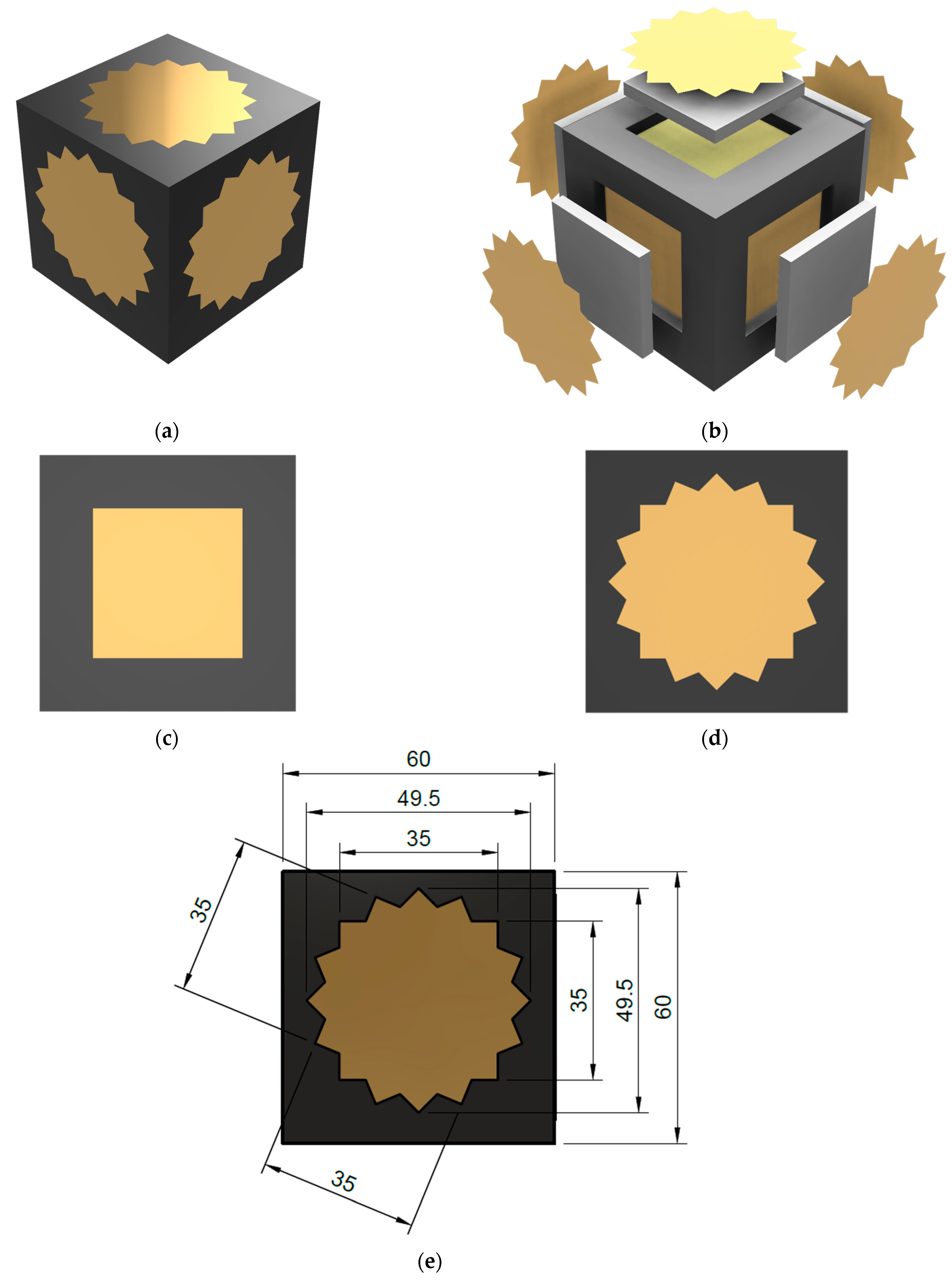
3.1.1. Antenna Design

The configuration of the proposed antenna is displayed in Figure 1. The antenna substrate has a cubic shape with a wall thickness of 4 mm. This design enables the internal volume to house the rectifier and matching circuits, fully integrating all rectenna components. Furthermore, the cubic shape facilitates the fabrication process through 3D printing, minimizing complexity and material waste. The antenna consists of five identical patch antennas located at the centers of five of the faces of the cube, each with a corresponding ground plane positioned directly beneath it on the opposite side of the substrate (within the cube), as shown in Figure 1b. Each patch is fed by a 50-ohm coax probe from behind the ground plane.
In the initial stage of the design process, we carefully defined the key performance requirements of the antenna in line with the overarching goal: to develop a compact, low-cost rectenna fabricated on a 3D-printed substrate, designed to capture electromagnetic energy from all directions in the 2.45 GHz Industrial, Scientific, and Medical (ISM) band, for powering next-generation sustainable IoT systems.
For the initial design, we selected a simple antenna geometry—a square patch (Figure 1c) and determined its approximate dimensions, based on the design formulas presented in [33], operating frequencies, and substrate permittivity. To minimize the overall size of the antenna, we created a composite substrate employing two materials with electromagnetic parameters presented in Table 1. Under the patch, as shown in Figure 1b, we utilized a resin-based material (εr′ = 2.789) to facilitate miniaturization. For the rest of the substrate, we selected PLA, a low-permittivity material (εr′ = 1.436) that provides an eco-friendly alternative and enhances the overall cost-efficiency of the fabrication process. Subsequently, the patch shape was modified, as shown in Figure 1d, to produce a compact and visually unobtrusive antenna, supporting linear polarization, with a bandwidth covering the 2.45 GHz ISM and low mutual coupling between ports. We optimized all critical antenna parameters—such as patch shape and size, ground plane dimensions, substrate thickness, and feed point location—through FDTD-based numerical simulations. During the optimization process, we varied one parameter at a time while keeping others constant to achieve the desired performance characteristics, including improved impedance matching, bandwidth, and radiation pattern. The final antenna dimensions, as determined through this optimization, are presented in Figure 1e. Additionally, Figure 1f–h shows the selected simulated reflection coefficient magnitudes (∣S11∣) for patch 1 (the front antenna) during the optimization process. The results in Figure 1f reveal that when the substrate is PLA only, the antenna has a narrow bandwidth due to the low relative permittivity of PLA. Furthermore, keeping all other antenna parameters unchanged (feed point, patch dimensions, etc.) and introducing the resin-based substrate under the patch, as shown in Figure 1b, leads, on the one hand, to a broadening of the bandwidth and a shift in the resonant frequency to higher frequency, and on the other hand, to a reduction in the matching, which necessitates optimization of the antenna elements. Figure 1g compares the ∣S11∣ curves for optimally and non-optimally positioned feed points, showing the impact of feed point placement on the antenna performance. Additionally, Figure 1h displays the ∣S11∣ curves for three patch sizes, demonstrating that the final dimensions (shown in Figure 1e) yield the best impedance matching and the widest bandwidth.

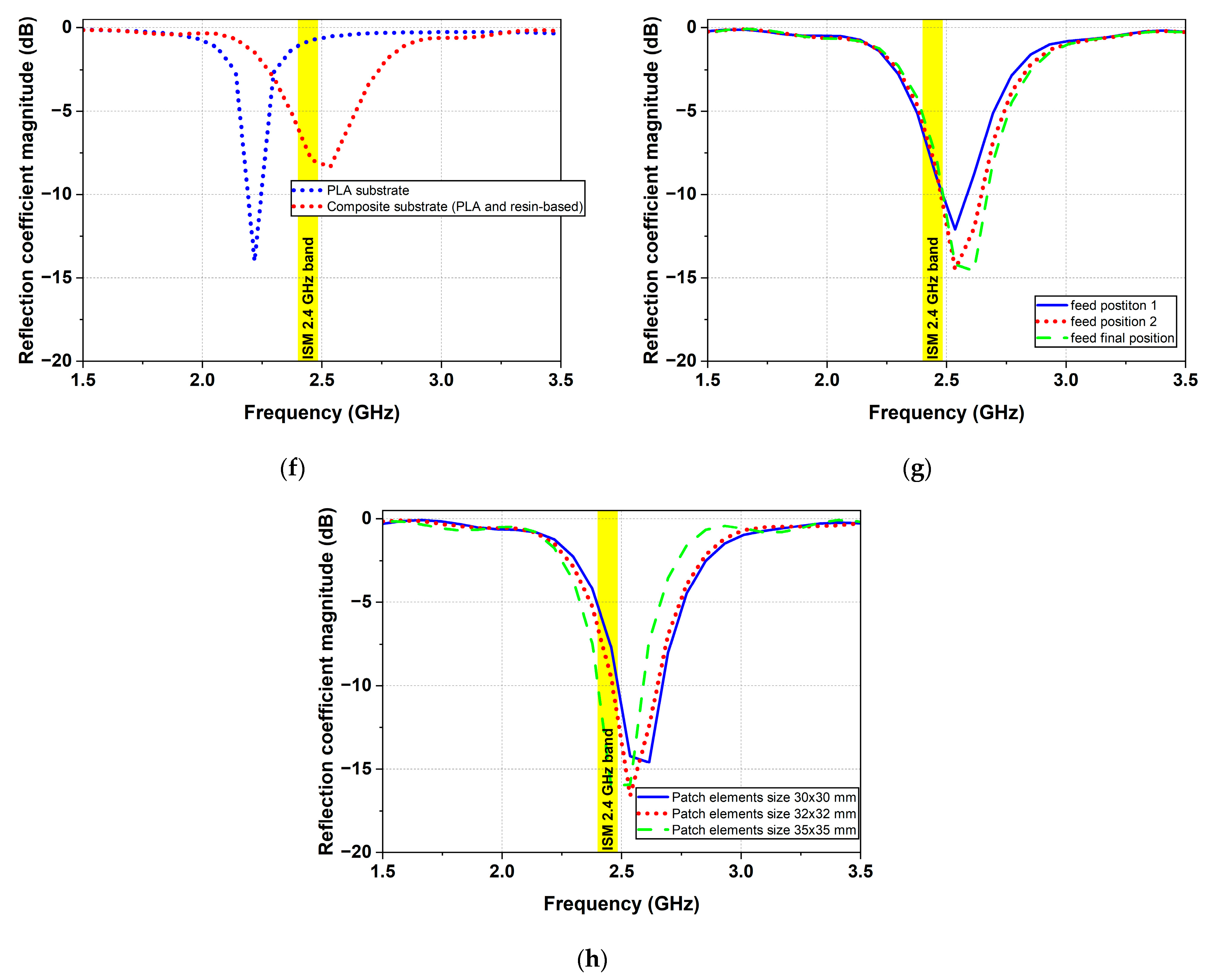
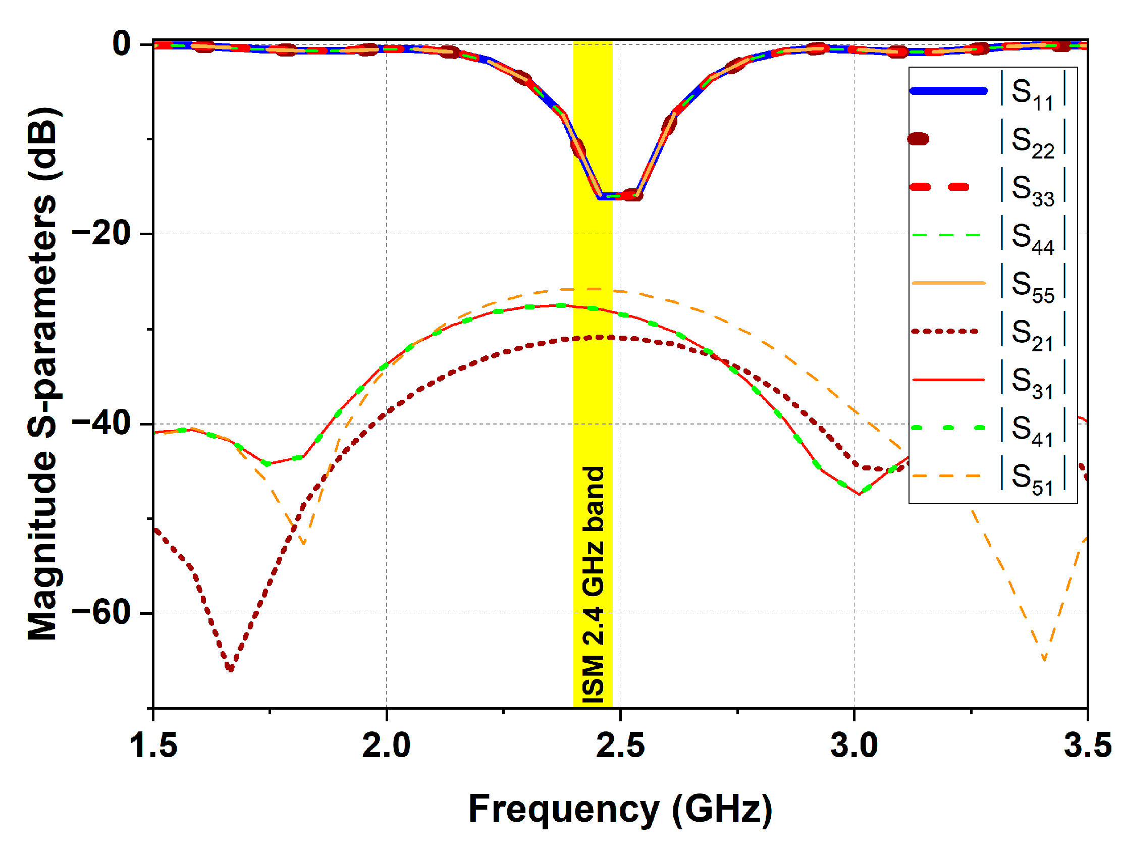
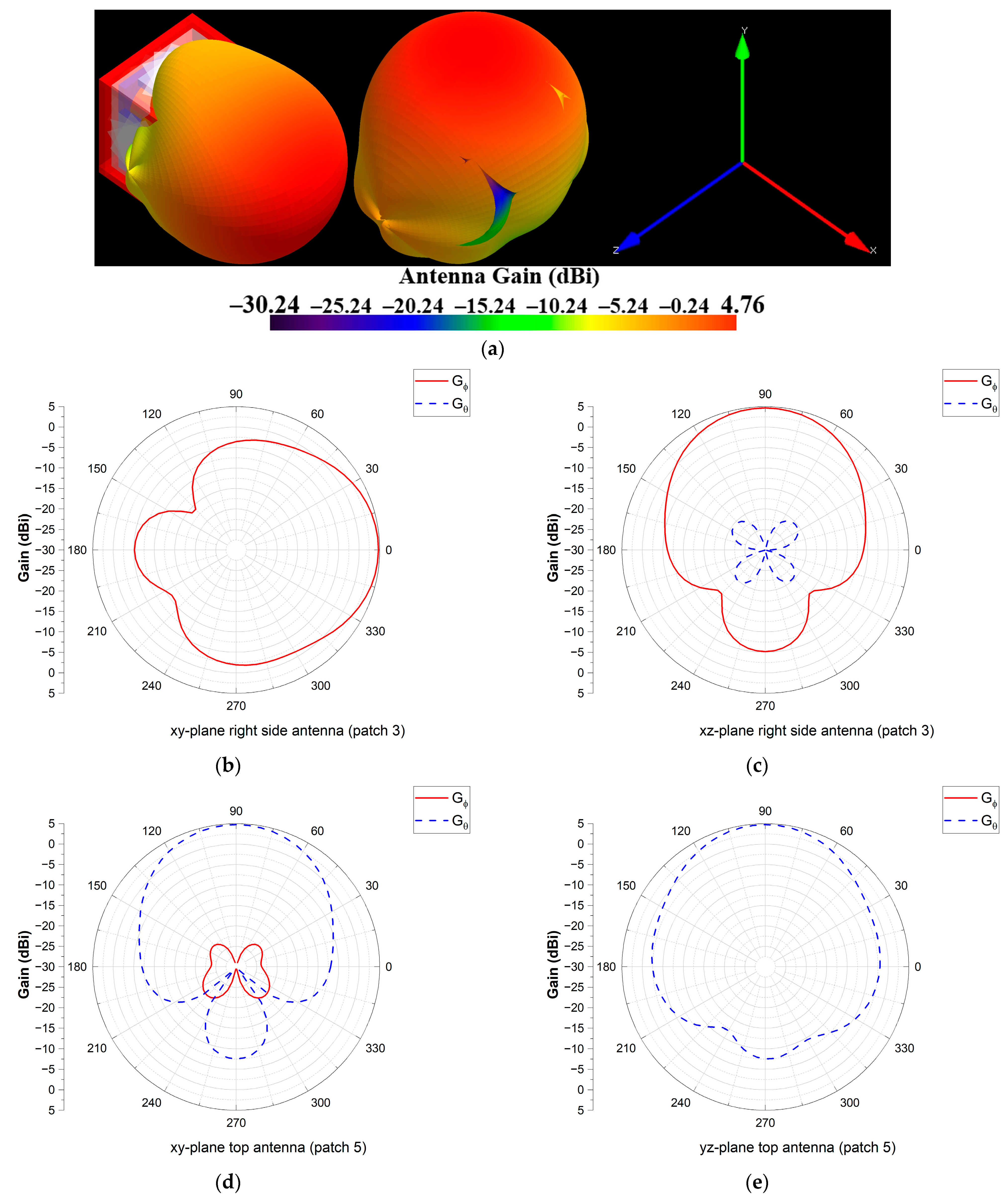
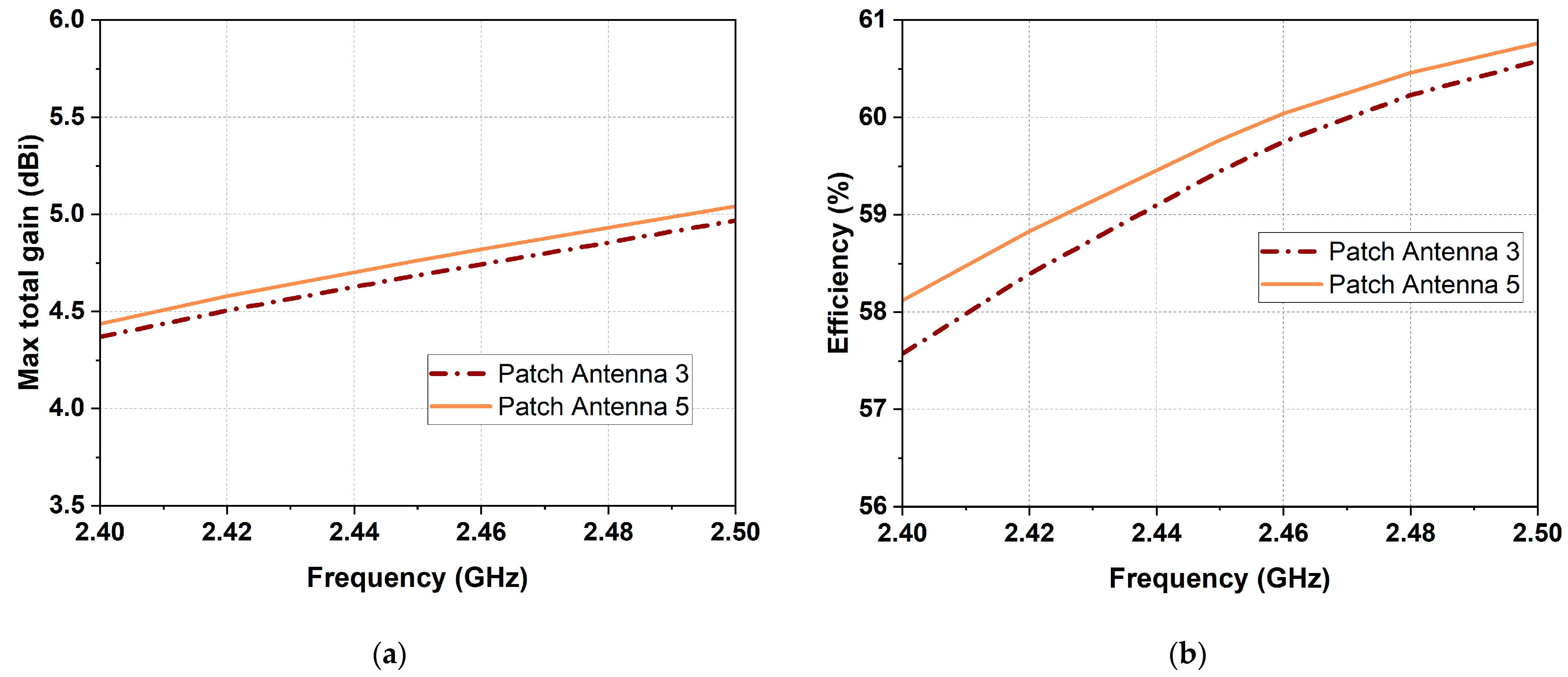
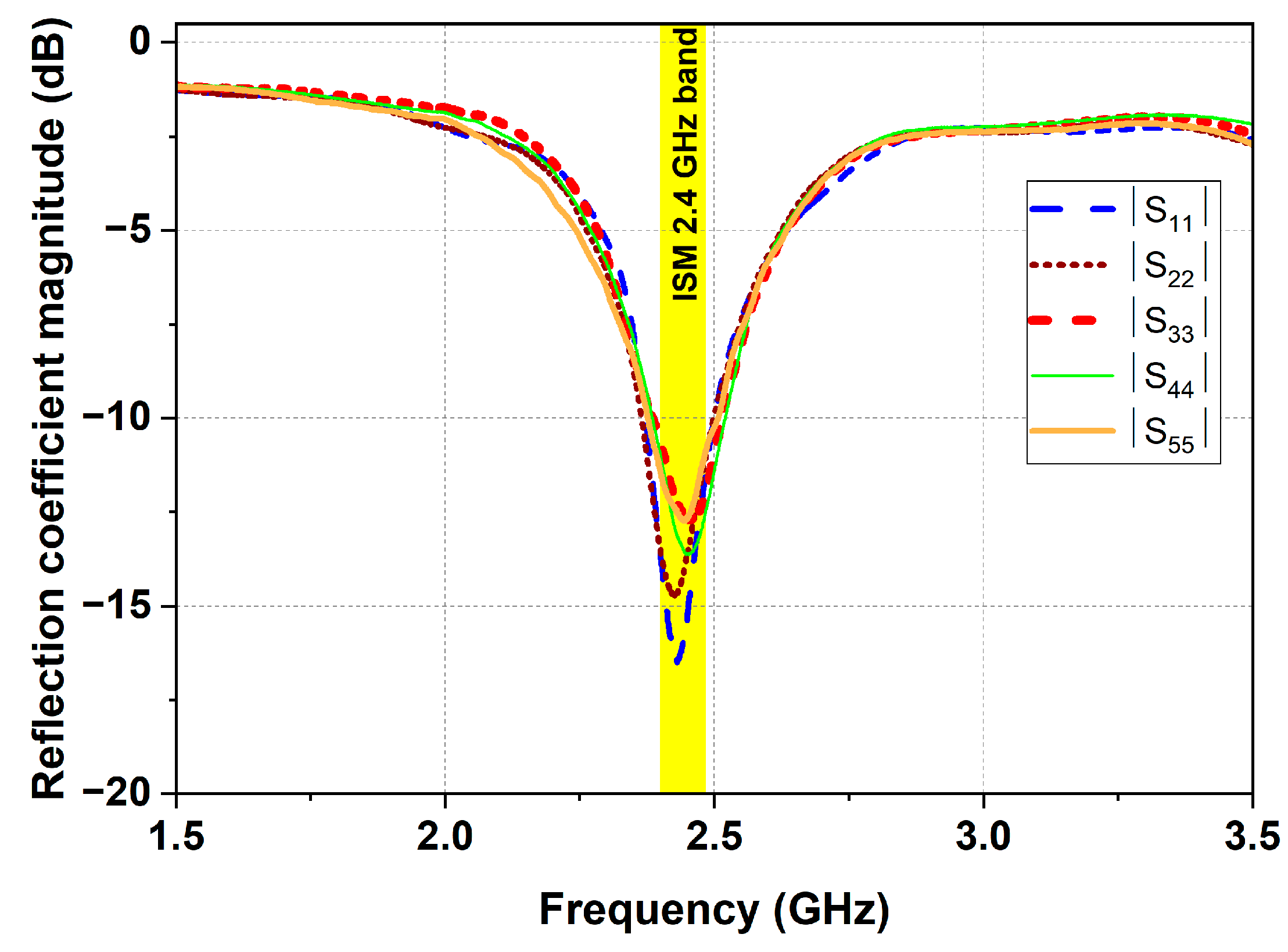
3.1.2. Antenna Performance

Figure 2 illustrates the reflection coefficients (∣S11∣ to ∣S55∣ in dB) and mutual coupling levels for each element of the proposed antenna. All five antennas exhibit reflection coefficient magnitudes below –10 dB across the target band, indicating good impedance matching. Moreover, due to the geometric symmetry of the design, we observe that all five antennas exhibit similar behavior, resonating at a frequency of 2.46 GHz. Also, each patch antenna achieves a bandwidth of 130 MHz within the frequency range of 2.4 GHz to 2.57 GHz. Additionally, the mutual coupling between adjacent patch antennas remains below −25 dB, demonstrating sufficient isolation and minimal interference. Among all patch combinations, the strongest mutual coupling is observed between patch 1 (front side) and patch 5 (top side) of the cube. Conversely, the weakest coupling occurs between patch 1 and patch 2, located on the front and back sides, respectively, likely due to their maximum spatial separation.
Due to the symmetrical nature of the rectenna design, as illustrated in Figure 1a,b and confirmed by the results in Figure 2, the performance in terms of gain, radiation pattern, and efficiency is analyzed in detail for two representative antennas (patches 3 and 5), as this is sufficient to demonstrate the behavior of the entire rectenna system.
Figure 3 presents the simulated 2D and 3D radiation patterns of the right side patch and top patch of the proposed antenna structure at 2.45 GHz. From Figure 3, we can see that each patch exhibits a unidirectional radiation pattern, resulting in a gain exceeding 4 dBi (see Figure 4a). This higher gain enables each antenna element to receive signals even in low-power-density environments. However, the unidirectional pattern also presents a limitation: each patch can harvest RF energy only from a specific direction (i.e., within a half-space). Nevertheless, by arranging five patch antennas on the faces of a cube (see Figure 1), this limitation is mitigated, allowing the proposed antenna to harvest RF energy from nearly all directions. Furthermore, because of the symmetry, all antenna elements exhibit the same radiation efficiency, ranging from 57.5% to 60.5% within the target frequency band, as shown in Figure 4b.

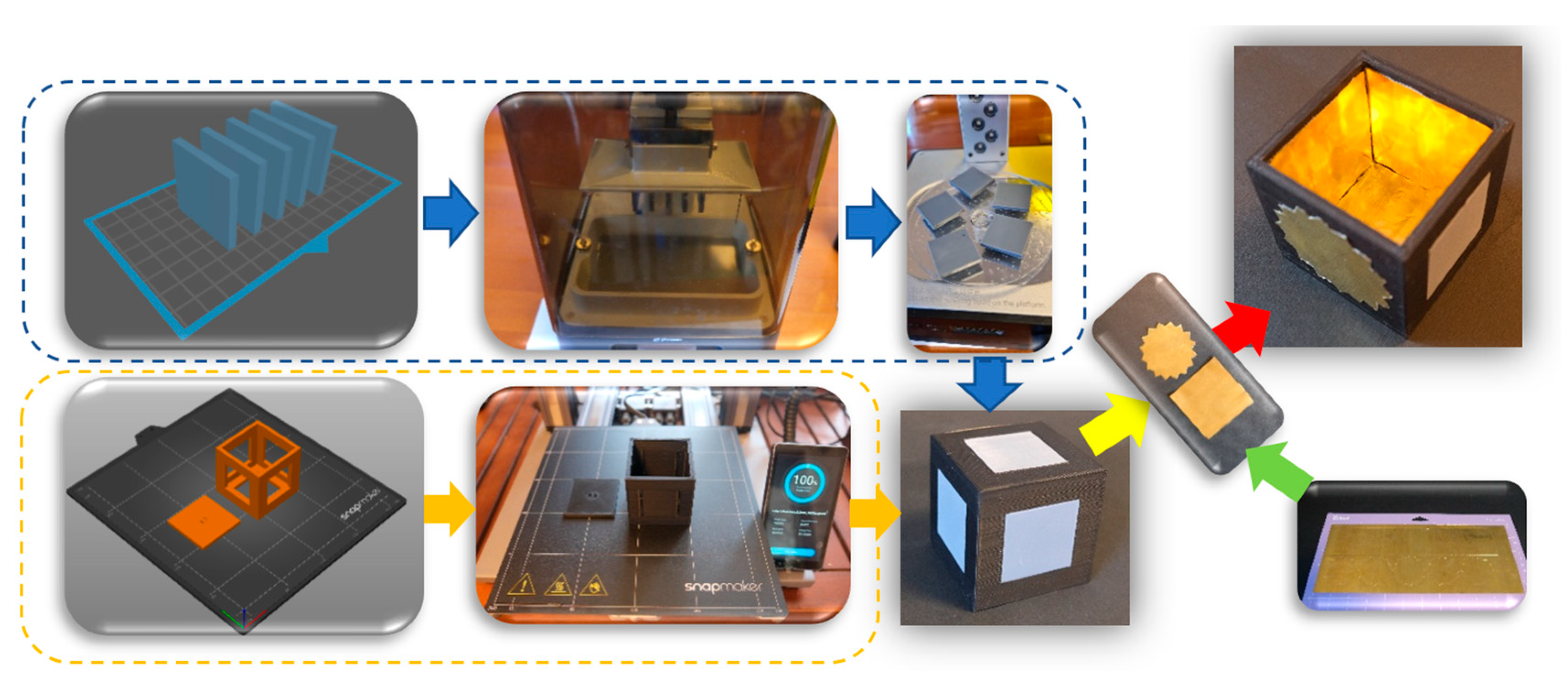
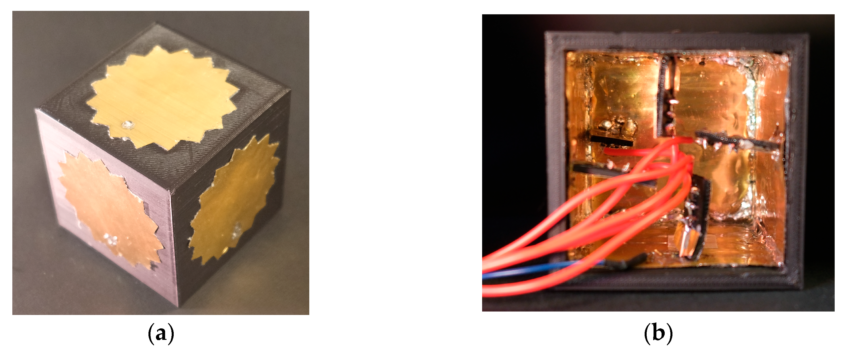
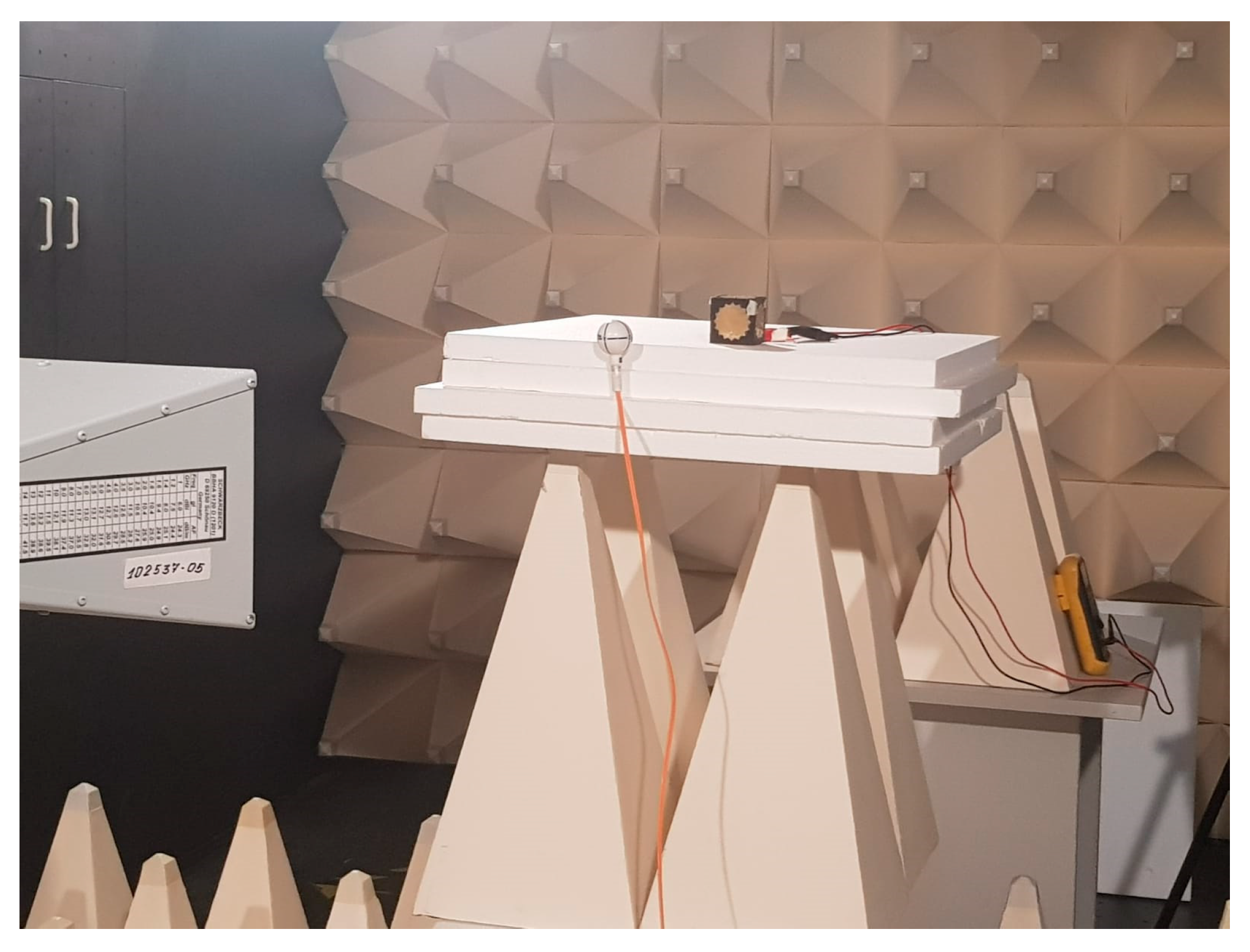
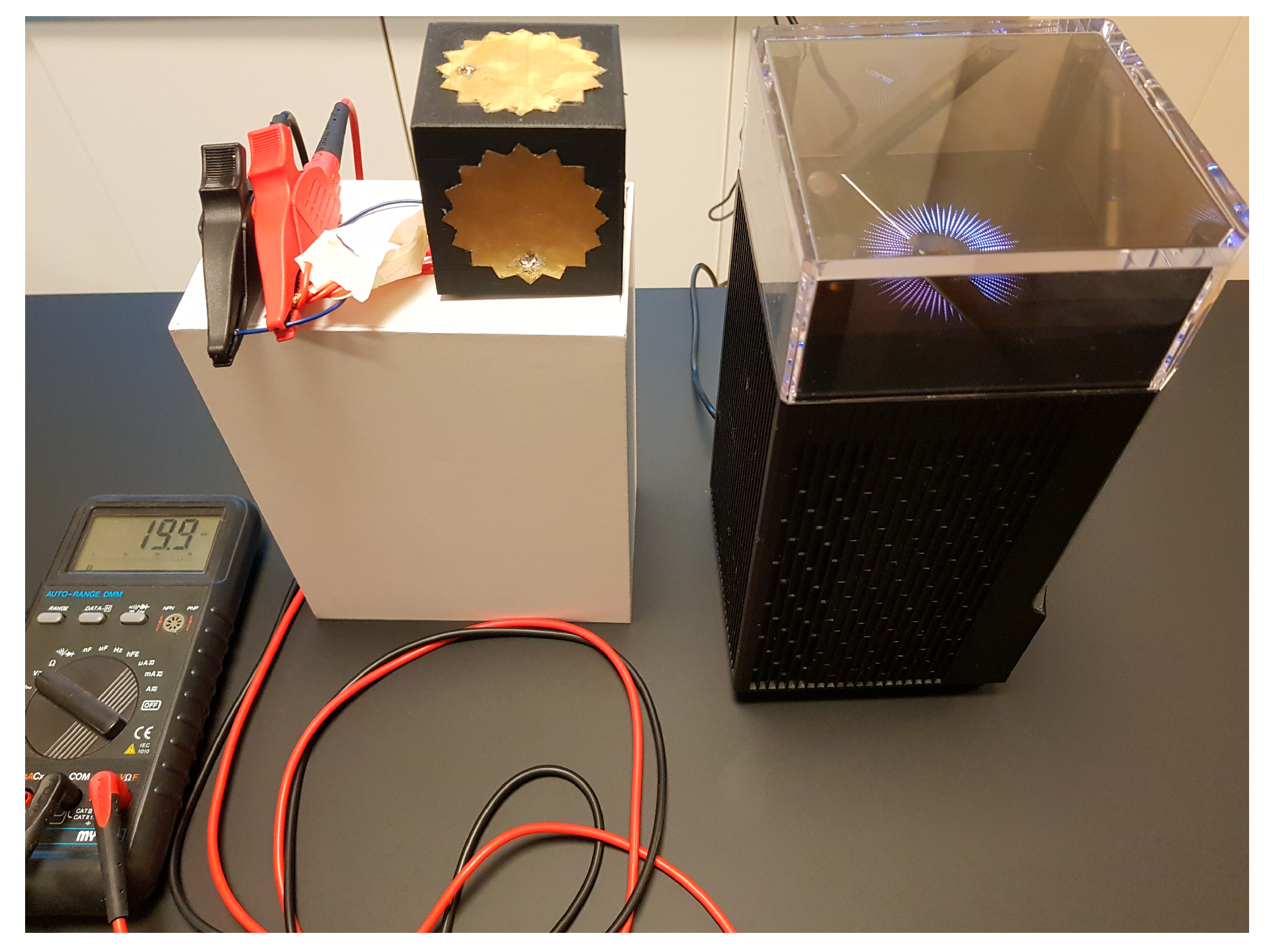
3.1.3. Antenna Prototype Fabrication and Measurements

The antenna prototype fabrication process includes the following stages: (1) fabrication of the antenna composite substrate using additive manufacturing; (2) precision cutting of the metallic elements; (3) assembly of the individual components; and (4) soldering of a coaxial cable to each port.
We used two distinct 3D printing technologies to fabricate the elements of the composite substrate: fused deposition modeling (FDM) with the Snapmaker A250 for PLA-based components and digital light processing (DLP) with the Phrozen Sonic Mini 4K for resin-based components. In the first step of the fabrication process, we developed digital models of the composite substrate components in Fusion 360, based on the final FDTD numerical simulation model. After completing the digital models in Fusion 360, we generated separate STL files for the resin-based and PLA-based components of the substrate to enable fabrication using different 3D printing technologies and materials. Using PrusaSlicer, we generated a G-code file compatible with the Snapmaker A250. At the same time, we used Chitubox to create a .ctb file for the Phrozen Sonic Mini 4K. We then transferred both files to their respective 3D printers for fabrication, as shown in Figure 5. After printing, we washed the fabricated resin-based substrate components using isopropyl alcohol and cured them under blanket UV light (see Figure 5). Additionally, we polished the fabricated PLA-based components to remove any roughness. In parallel, we precisely cut the antenna’s metal components (patches and ground planes) from brass foil with an accuracy of 0.01 mm using a Cricut Explore Air 2 cutting machine. Next, we assembled the two parts of the composite substrate. After that, we added the metallic elements of the antenna, as illustrated in Figure 5. In the final stage, each patch antenna was connected to a 50-ohm coaxial feed line terminated with a U.FL connector. The outer conductor was soldered to the ground plane. The center conductor penetrated both the substrate and the patch and was soldered to the top surface of the patch at a location determined through FDTD numerical simulations to ensure optimal impedance matching.
In order to verify the numerical simulations, we measured the reflection coefficients and mutual coupling of each patch antenna in the fabricated prototype using a vector network analyzer (VNA). Before measurements, we calibrated the VNA across the 1.5–3.5 GHz frequency range using the short–open–load (SOL) calibration procedure. For high-precision characterization of the rectenna elements, we selected a resolution of 100,001 data points. All measurements were conducted in a semi-anechoic chamber to minimize external interference. The results in Figure 6 show that all five patch antennas cover the target frequency band from 2.4 to 2.5 GHz, exhibiting ∣S11∣, ∣S22∣, ∣S33∣, ∣S44∣, and ∣S55∣ values of less than −10 dB. In addition, the geometric symmetry of the design results in all five ports resonating at a frequency of 2.42 to 2.46 GHz. Furthermore, the measurement results agree well with those from the FDTD numerical calculations, which validates the design methodology.

3.2. Rectifier Design and Performance Evaluation

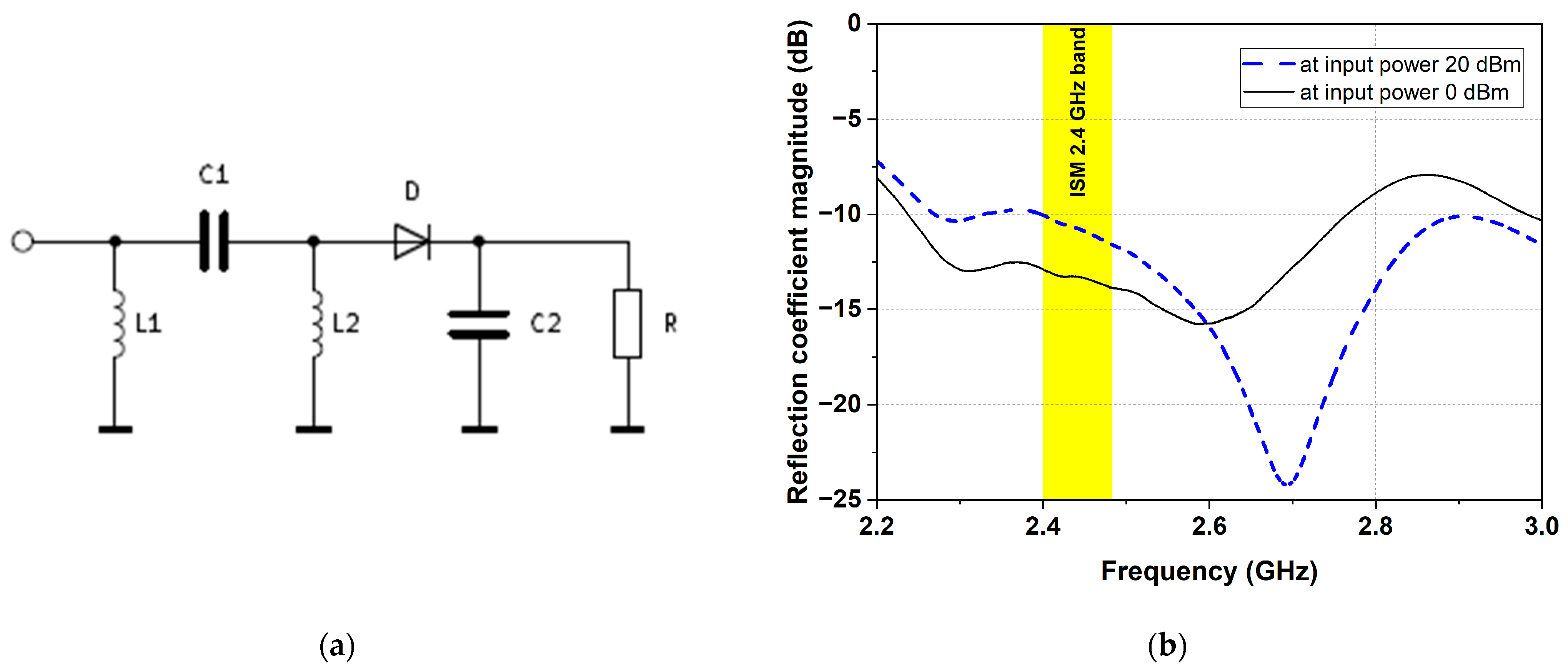
3.2.1. Rectifier Design

Figure 7a displays the schematic of the overall rectifier circuit. In this proposed design, each of the five patch antennas is connected to an individual single-series rectifier circuit, allowing for simultaneous energy harvesting from multiple input ports. We decided to use the single-series rectifier topology on a biodegradable substrate made from PLA due to its effective balance of circuit simplicity, cost efficiency, and reliable RF-to-DC conversion [34]. Moreover, using five independent rectifiers enables the summation of their DC output voltages without the interference commonly found in AC circuits. In Section 6, we demonstrated the benefit of this approach (simultaneous DC voltage summation) in a typical indoor RF environment. As a rectifying element, we selected the Schottky diode NSVR351SDSA3. Following the selection of the rectifying component, we developed the matching network using SMD elements and employing an iterative procedure that combines simulation-driven modeling with experimental data obtained from experimental measurements of prototypes [35]. To establish the final values of the components, we fabricated several prototypes and thoroughly tested them. Figure 7b presents the measured reflection coefficient of the single rectifier circuit at input power levels of 0 dBm and 20 dBm using a VNA calibrated in the frequency range from 2.2 GHz to 3 GHz. The selected values of L1 = 68 nH, L2 = 33 nH, and C1 = 1 pF ensure impedance matching between the antenna and the rectifying circuit across the target frequency band. Additionally, C2 = 47 pF suppresses higher-order harmonics while allowing DC to pass through. The results indicate that the rectifier achieves good impedance matching across the target frequency range for those power levels.

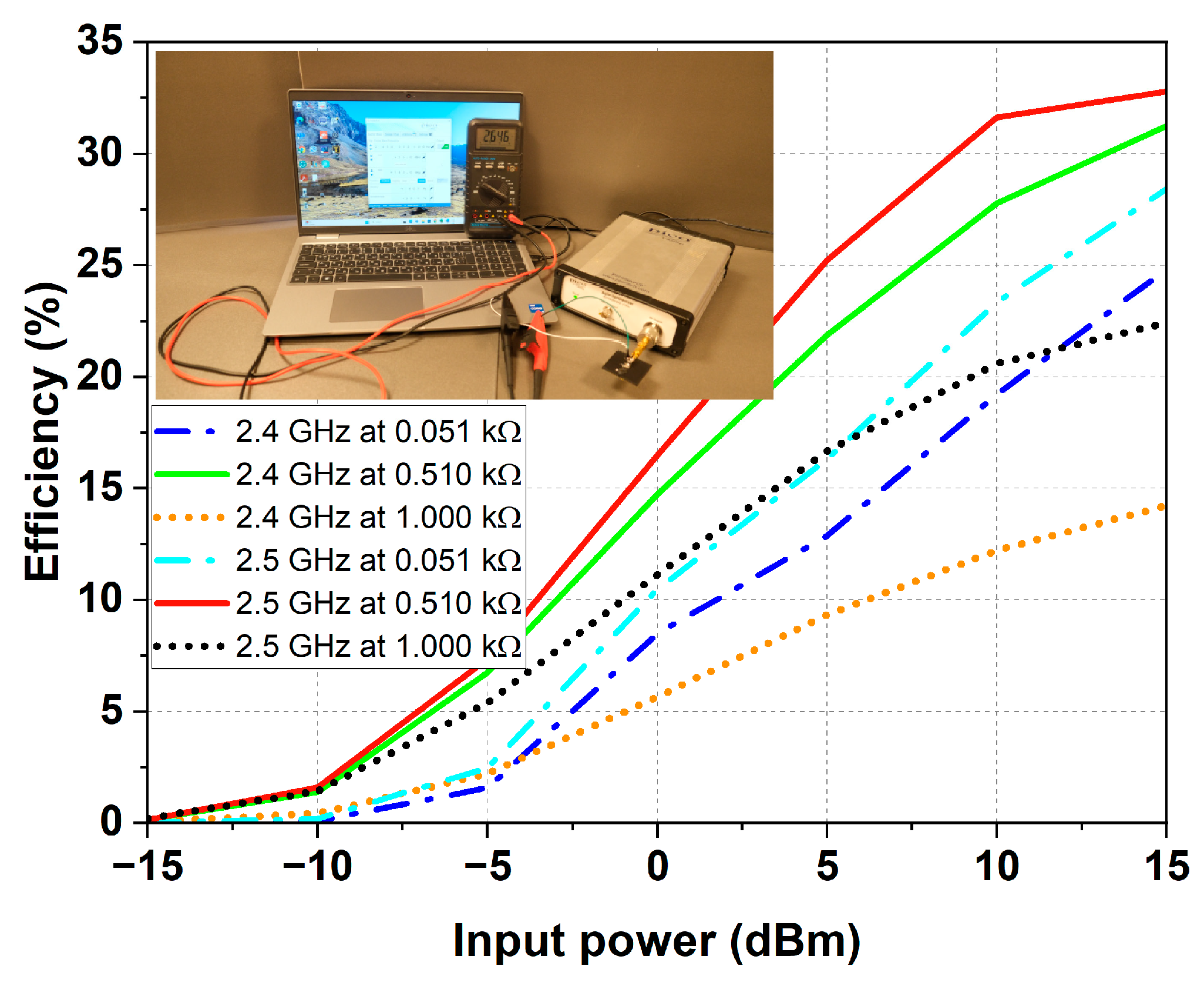
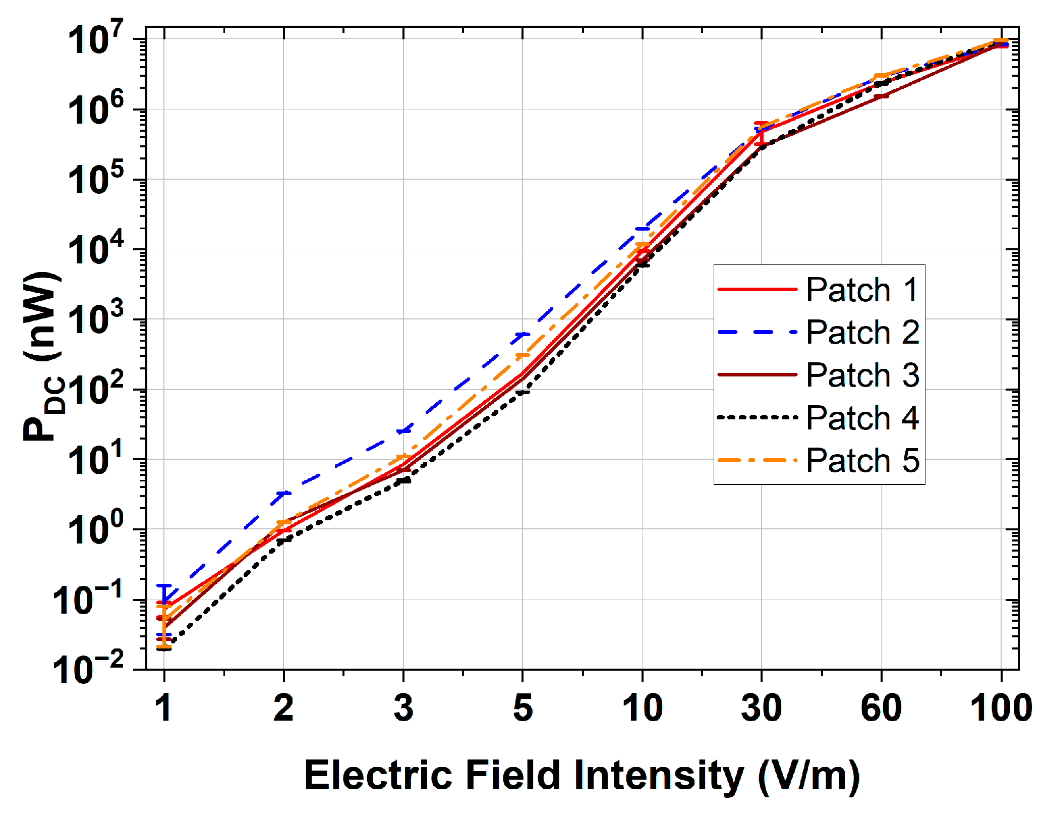
3.2.2. Rectifier Performance Evaluation

Figure 8 presents the rectifier RF-to-DC conversion efficiency (ηrectifier) results and a photograph of the measurement setup. Initially, we measured the DC voltage across load resistances of 0.051 kΩ, 0.51 kΩ, and 1.0 kΩ at two frequencies, 2.4 GHz and 2.5 GHz, with input RF power levels varying from −15 dBm to +15 dBm. After that, we calculated the corresponding RF-to-DC conversion efficiency values using Equation (1), as detailed below.
ηrectifier (%) = (PDC/Pin) × 100,
where Pin is the input RF power from a microwave generator, measured in watts, and PDC is the output DC power calculated using Equation (2)
PDC = V2DC/RL,
where VDC is measured DC voltage, and RL is the load resistance in Ω.
The results indicate that the rectifier circuit conversion efficiency increases with increasing input RF power, making it suitable for dedicated RF energy harvesting applications. Moreover, the RF-to-DC conversion efficiency remains below 1% when the input power is less than –15 dBm for all the examined load resistance values. At such low power levels, the Schottky diode likely operates outside its optimal range for efficient RF-to-DC conversion [36]. Also, for a load value of 0.51 kΩ, the RF-to-DC efficiency is highest across all input power levels, reaching up to 33% at an input power of +15 dBm and a frequency of 2.5 GHz. Hence, potential use cases include short-range and controlled environment applications, such as smart homes or industrial setups, where the rectenna can be placed within 0.5 m of the RF source, as shown in Section 6.

4. Rectenna Measurements

To validate the proposed design, we fabricated a prototype. To prototype the rectenna, we fabricated the proposed compact cubic-shape antenna on a 3D-printed composite substrate and connected each of the five patches to a rectifier circuit, as shown in Figure 7a, to allow simultaneous energy harvesting from multiple input ports. The photographs of the fabricated rectenna prototype are presented in Figure 9. As shown in Figure 9a, the final optimized design was compact and visually unobtrusive. In addition, Figure 9b demonstrates that the proposed design provided sufficient internal volume to house the rectifier and matching networks, enabling the full integration of all rectenna components.
We evaluated the performance of the rectenna within a semi-anechoic chamber. Initially, we measured the DC voltage output at each rectenna port as a function of electric field intensity for four frequencies: 2.35 GHz, 2.4 GHz, 2.45 GHz, and 2.5 GHz. Figure 10 shows a photograph of the experimental setup. To create a uniform electric field with an intensity ranging from 1 V/m to 100 V/m, a vertically oriented horn antenna was used, connected to a power amplifier and driven by a microwave signal generator. An isotropic probe was used to establish the electric field intensity and to monitor the field during the measurements. Figure 11 illustrates the output DC power (PDC), derived from the measured DC voltage at the first rectenna output, plotted against the electric field intensity for four frequencies. As anticipated, the PDC increases with the electric field intensity, as shown in Figure 11. Additionally, the results suggest that the PDC remains relatively consistent across all frequencies within the ISM 2.45 GHz band. It is also observed that the antenna efficiently converts radio frequency power at frequencies outside the designated band, particularly at 2.35 GHz.
Figure 12 presents PDC versus electric field intensity of all antennas at 2.45 GHz. The results show that the PDC of all antenna ports is almost the same, confirming that the proposed rectenna can harvest RF energy from nearly all directions. Moreover, experimental results from the fabricated rectenna prototype validate its capability to power low-power devices effectively.

5. Performance Comparison of the Proposed Rectenna with Other 3D-Printed Rectennas

To demonstrate the advantages of the proposed rectenna, we compared its key performance metrics with those of other rectennas fabricated on 3D-printed substrates. From Table 2, it is evident that our design features the smallest dimensions among those presented in [1,23,29,30,31], achieves higher efficiency than the rectenna in [21], and offers wider bandwidth in comparison to [31]. Its maximum conversion efficiency is also comparable to that reported in [23]. The proposed rectenna also employs linear polarization, matching the polarization of typical Wi-Fi access point antennas [37,38], as well as most rectennas designed for indoor RF energy harvesting [23,29,30]. In this case, the linear polarization ensures maximum power extraction from incident waves and minimal polarization mismatch when the rectenna is in indoor environments, particularly near Wi-Fi routers and household electronics such as laptops, smart TVs, and other devices emitting in the ISM 2.45 GHz band. Similar to the designs in [21,29,30], the proposed rectenna combines aesthetic appeal, low cost, and ease of fabrication. Moreover, our design is the only one that enables the internal rectenna volume to accommodate both the rectifier and matching circuits, fully integrating all rectenna components. The proposed visually unobtrusive design not only enhances compactness but also allows the proposed rectenna to harvest RF energy from nearly all directions, highlighting the novelty of our work.

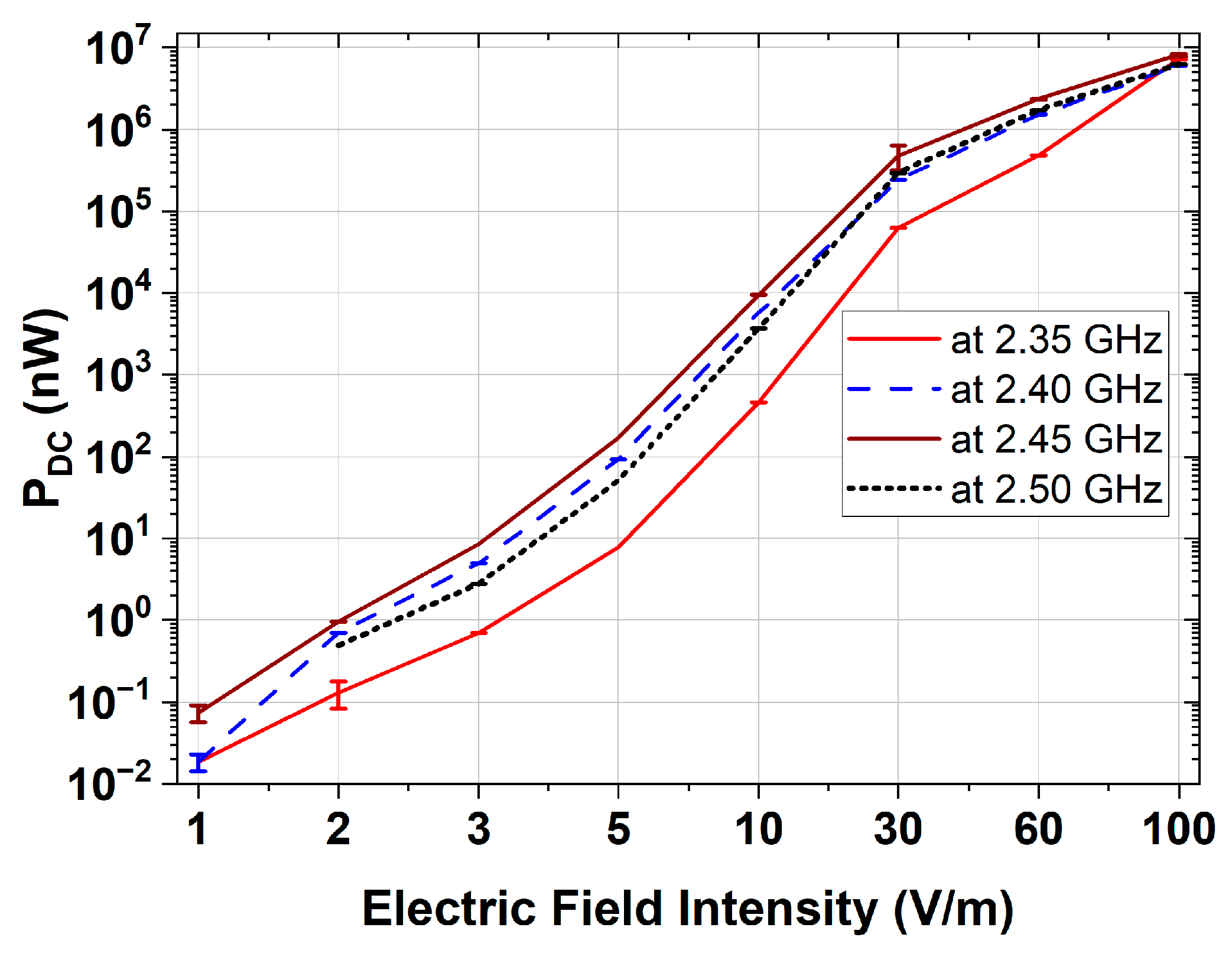
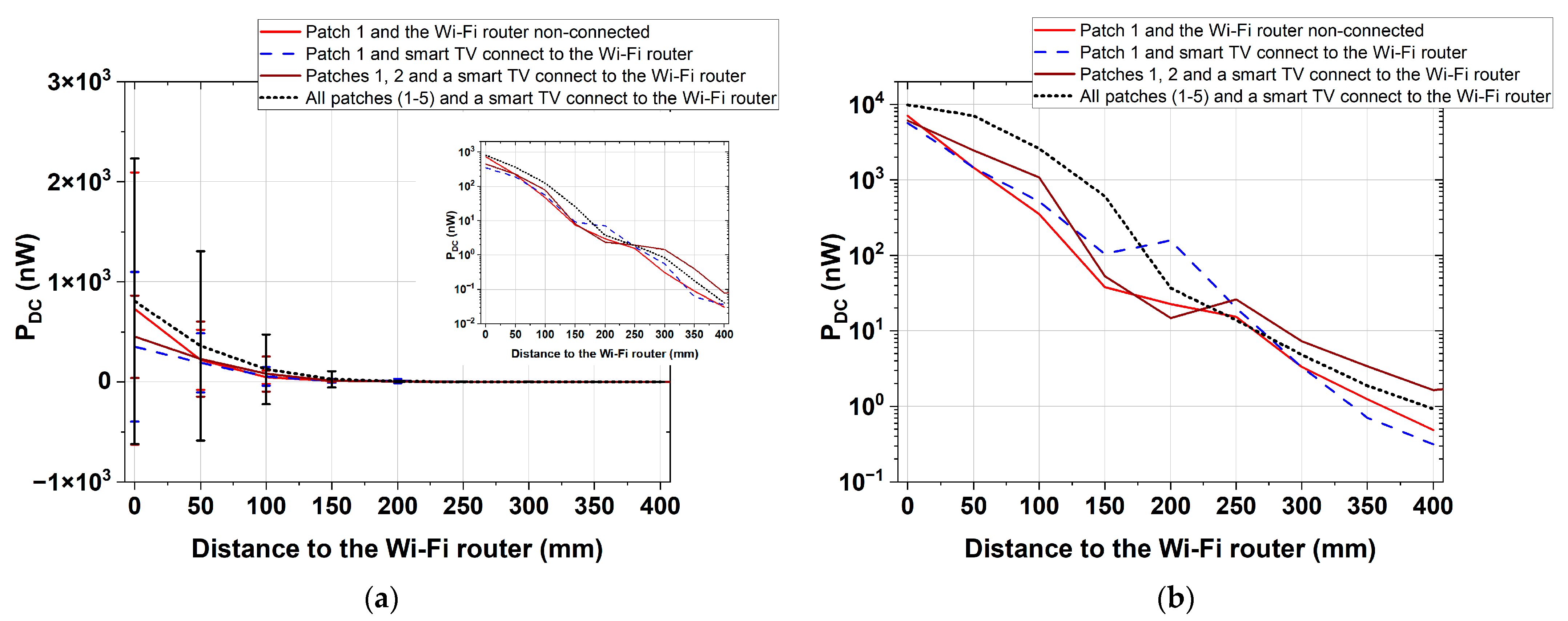
6. Rectenna Testing in a Typical Indoor RF Environment

Finally, to demonstrate the applicability of the rectenna, we performed DC voltage measurements in an apartment equipped with a 2.4 GHz commercial Wi-Fi router serving as the access point, representing a typical indoor RF environment. During the measurements, we positioned the rectenna at the same height as the router’s antennas. We varied the distance between the rectenna and the router from 0 mm to 400 mm in increments of 50 mm, as illustrated in Figure 13. This setup simulated common deployment scenarios such as smart home environments and indoor sensor networks. We performed measurements in two scenarios: (1) with no connected end devices (e.g., laptop, smart TV) and (2) with a smart TV connected to the router, streaming a 4K Netflix movie.
At each distance, we measured and recorded the DC voltage for one minute. Figure 14a shows the averaged values, whereas Figure 14b shows the maximum values.
Additionally, to highlight the advantages of simultaneous DC voltage summation, Figure 14a,b compare the rectenna’s performance when harvesting RF energy from a single antenna versus two and all five antennas collectively. The results demonstrate that the rectenna effectively harvests RF energy up to approximately 400 mm from the router, with a decrease in collected power at greater distances, primarily due to free-space path loss and multipath fading. Furthermore, when using only one antenna, the collected power is less compared to that of all antennas. These results confirm that the proposed rectenna is suitable for wireless energy harvesting in both near-field and mid-range indoor environments, supporting its potential application in powering the next generation of low-power, sustainable IoT devices.

7. Conclusions

This paper presents a compact cubic-shaped rectenna on a 3D-printed composite substrate consists of five identical patch antennas located at the centers of five of the faces of the cube, each with a corresponding ground plane positioned directly beneath it on the opposite side of the substrate, allowing the proposed antenna to harvest RF energy from nearly all directions. Each of the five patch antennas was connected to a single-series rectifier circuit, allowing for simultaneous energy harvesting from multiple input ports. The proposed antenna was fabricated using two 3D printing technologies: FDM and DLP. Furthermore, due to the symmetry, each patch antenna achieves a bandwidth of 130 MHz in the frequency range of 2.4 GHz to 2.57 GHz and a maximum efficiency of 60.5%. Additionally, a good isolation of below −25 dB between adjacent patch antennas is achieved. The results also indicate that the rectifier achieves good impedance matching across the target frequency range for two power levels. Moreover, the rectifier circuit measurements show that maximum conversion efficiency is 33%, comparable to that of the reported rectennas fabricated on 3D-printed substrates. Furthermore, our design is unobtrusive and uniquely capable of accommodating both the rectifier and matching circuits within the internal rectenna volume, fully integrating all rectenna components using eco-friendly materials and additive manufacturing. Additionally, the rectenna is capable of harvesting RF energy in indoor real-world scenarios. The results confirm that the proposed rectenna is suitable for wireless energy harvesting in both near-field and mid-range indoor environments, supporting its potential application in powering the next generation of low-power, sustainable IoT devices.

Author Contributions

Conceptualization, N.A., B.A. and G.A.; methodology, N.A., B.A. and G.A.; software, N.A. and B.A.; validation, N.A., B.A. and G.A.; formal analysis, N.A. and G.A.; investigation, N.A., B.A. and G.A.; resources, N.A. and G.A.; data curation N.A., B.A. and G.A.; writing—original draft preparation, G.A.; writing—review and editing, N.A. and B.A.; visualization, B.A. and N.A.; supervision, G.A.; project administration, G.A.; funding acquisition, G.A. and N.A. All authors have read and agreed to the published version of the manuscript.

Funding

This research was funded by the BULGARIAN NATIONAL SCIENCE FUND at the Ministry of Education and Science, Bulgaria, grant number KP-06-H57/11 from 16 November 2021, “Antenna structures for new energy sources in next-generation wireless networks”.

Data Availability Statement

The data presented in this study are available upon request from the authors.

Conflicts of Interest

The authors declare no conflicts of interest.

Abbreviations

The following abbreviations are used in this manuscript:
IoTInternet of Things
RF-EHRadio frequency energy harvesting
WPTWireless power transmission
PLAPolylactic acid
3DThree dimensional
FDTD Finite-difference time-domain method
ISM Industrial, scientific, and medical
FDMFused deposition modeling
DLPDigital light processing
STLStandard triangle language
RFRadio frequency
DCDirect current
SMDSurface-mounted device

References

  1. Next Generation Internet of Things. Available online: https://digital-strategy.ec.europa.eu/en/policies/next-generation-internet-things (accessed on 5 May 2025).
  2. Fattahi, A. IoT and Digital Transformation. In IoT Product Design and Development: Best Practices for Industrial, Consumer, and Business Applications; Wiley: Hoboken, NJ, USA, 2023; pp. 9–21. [Google Scholar]
  3. Zhi, Z.; Wu, Q. Wearable IoT System for Hand Function Assessment Based on EMG Signals. Electronics 2024, 13, 778. [Google Scholar] [CrossRef]
  4. Atanasova, G.L.; Atanasov, B.N.; Atanasov, N.T. Fully Textile Dual-Band Logo Antenna for IoT Wearable Devices. Sensors 2022, 22, 4516. [Google Scholar] [CrossRef] [PubMed]
  5. Poyyamozhi, M.; Murugesan, B.; Rajamanickam, N.; Shorfuzzaman, M.; Aboelmagd, Y. IoT—A Promising Solution to Energy Management in Smart Buildings: A Systematic Review, Applications, Barriers, and Future Scope. Buildings 2024, 14, 3446. [Google Scholar] [CrossRef]
  6. Biswas, A.; Wang, H.-C. Autonomous Vehicles Enabled by the Integration of IoT, Edge Intelligence, 5G, and Blockchain. Sensors 2023, 23, 1963. [Google Scholar] [CrossRef]
  7. Atanasov, B.N.; Atanasov, N.T.; Atanasova, G.L. Reliable and Resilient Wireless Communications in IoT-Based Smart Agriculture: A Case Study of Radio Wave Propagation in a Corn Field. Telecom 2024, 5, 1161–1178. [Google Scholar] [CrossRef]
  8. Kamatchi Sundari, V.; Nithyashri, J.; Kuzhaloli, S.; Subburaj, J.; Vijayakumar, P.; Hency Jose, P.S. Comparison analysis of IoT based industrial automation and improvement of different processes—Review. Mater. Today Proc. 2021, 45, 2595–2598. [Google Scholar] [CrossRef]
  9. Statista. Number of Internet of Things (IoT) Connections Worldwide from 2022 to 2023, with Forecasts from 2024 to 2033. Available online: https://www.statista.com/statistics/1183457/iot-connected-devices-worldwide/ (accessed on 10 May 2025).
  10. GSMA Intelligence. IoT Connections Forecast to 2030. Available online: https://www.gsmaintelligence.com/research/iot-connections-forecast-to-2030 (accessed on 30 December 2023).
  11. Atanasov, N.T.; Atanasov, B.N.; Atanasova, G.L. Electromagnetic Properties of Natural Plant Leaves for Eco-Friendly and Biodegradable Substrates for Wireless IoT Devices. Sensors 2025, 25, 1118. [Google Scholar] [CrossRef]
  12. Sharma, N.; Panwar, D. Green IoT: Advancements and Sustainability with Environment by 2050. In Proceedings of the 2020 8th International Conference on Reliability, Infocom Technologies and Optimization (Trends and Future Directions) (ICRITO), Noida, India, 5–6 June 2020. [Google Scholar]
  13. Tahiliani, V.; Dizalwar, M. Green IoT Systems: An Energy Efficient Perspective. In Proceedings of the Eleventh International Conference on Contemporary Computing (IC3), Noida, India, 2–4 August 2018; pp. 1–6. [Google Scholar]
  14. López, O.L.A.; Rosabal, O.M.; Ruiz-Guirola, D.E.; Raghuwanshi, P.; Mikhaylov, K.; Lovén, L.; Iyer, S. Energy-Sustainable IoT Connectivity: Vision, Technological Enablers, Challenges, and Future Directions. IEEE Open J. Commun. Soc. 2023, 4, 2609–2666. [Google Scholar] [CrossRef]
  15. Rahmani, H.; Shetty, D.; Wagih, M.; Ghasempour, Y.; Palazzi, V.; Carvalho, N.B.; Correia, R.; Costanzo, A.; Vital, D.; Alimenti, F.; et al. Next-Generation IoT Devices: Sustainable Eco-Friendly Manufacturing, Energy Harvesting, and Wireless Connectivity. IEEE J. Microw. 2023, 3, 237–255. [Google Scholar] [CrossRef]
  16. Nusrat, T.; Roy, S.; Lotfi-Neyestanak, A.A.; Noghanian, S. Far-Field Wireless Power Transfer for the Internet of Things. Electronics 2023, 12, 207. [Google Scholar] [CrossRef]
  17. Liao, L.; Li, Z.; Tang, Y.; Chen, X. Dual-Polarized Stacked Patch Antenna for Wireless Communication Application and Microwave Power Transfer. Electronics 2021, 10, 2988. [Google Scholar] [CrossRef]
  18. Niotaki, K.; Carvalho, N.B.; Georgiadis, A.; Gu, X.; Hemour, S.; Wu, K.; Matos, D.; Belo, D.; Pereira, R.; Figueiredo, R.; et al. RF Energy Harvesting and Wireless Power Transfer for Energy Autonomous Wireless Devices and RFIDs. IEEE J. Microw. 2023, 3, 763–782. [Google Scholar] [CrossRef]
  19. Deng, X.; Yang, P.; Chen, S.; Ren, W. Design of a 2.4 & 5.8 GHz Efficient Circularly Polarized Rectenna for Wireless Power Transfer Applications. Electronics 2023, 12, 2645. [Google Scholar] [CrossRef]
  20. Jing, J.; Yang, B.; Yan, L.; Shinohara, N.; Liu, C. Fully Polarized Wideband Omnidirectional RF Harvester with Highly Efficient DC Power Combination. Electronics 2024, 13, 4891. [Google Scholar] [CrossRef]
  21. Atanasov, B.; Atanasov, N.; Atanasova, G. A Multi-Band Antenna with an Aesthetic Design for Ambient RF Energy Harvesting. In Proceedings of the 2023 17th European Conference on Antennas and Propagation (EuCAP), Florence, Italy, 26–31 March 2023. [Google Scholar]
  22. Prashad, L.; Mohanta, H.C.; Mohamed, H.G. A Compact Circular Rectenna for RF-Energy Harvesting at ISM Band. Micromachines 2023, 14, 825. [Google Scholar] [CrossRef]
  23. Patil, D.D.; Subramanian, K.S.; Pradhan, N.C.; Varadharaj, E.K.; Senthilkumaran, K.; Murugesan, M. 3D-printed dual-band energy harvester for WSNs in green IoT applications. AEU Int. J. Electron. Commun. 2023, 164, 154641. [Google Scholar] [CrossRef]
  24. Jalali, Z.; Hasani, P.; Hashemi, S.M.; Ghalamkari, B. A multiband coplanar based circularly polarized rectenna with high efficiency for IOT energy harvesting Applications. AEU Int. J. Electron. Commun. 2023, 170, 154796. [Google Scholar] [CrossRef]
  25. Sang, J.; Qian, L.; Wang, X.; Shi, G. A dual-band omnidirectional rectenna for radio-frequency energy harvesting applications. Microelectron. J. 2025, 156, 106533. [Google Scholar] [CrossRef]
  26. Shen, S.; Zhang, Y.; Chiu, C.; Murch, R.D. A compact quad-port dual-polarized dipole rectenna for ambient RF energy harvesting. In Proceedings of the 12th European Conference on Antennas and Propagation (EuCAP 2018), London, UK, 9–13 April 2018. [Google Scholar]
  27. Mansour, M.M.; Torigoe, S.; Yamamoto, S.; Kanaya, H. Compact and Simple High-Efficient Dual-Band RF-DC Rectifier for Wireless Electromagnetic Energy Harvesting. Electronics 2021, 10, 1764. [Google Scholar] [CrossRef]
  28. Bolognesi, M.; Prosa, M.; Seri, M. Biocompatible and Biodegradable Organic Electronic Materials. In Electronic and Optical Materials, Sustainable Strategies in Organic Electronics; Marrocchi, A., Ed.; Woodhead Publishing: Cambridge, UK, 2022; pp. 297–338. [Google Scholar]
  29. Atanasov, N.; Atanasov, B.; Atanasova, G. Design, Fabrication and Performance Evaluation of Antennas for Smart Urban Agriculture. In Proceedings of the 2024 Advanced Topics on Measurement and Simulation (ATOMS), Constanta, Romania, 15–17 May 2024. [Google Scholar]
  30. Jun, S.Y.; Elibiary, A.; Sanz-Izquierdo, B.; Winchester, L.; Bird, D.; McCleland, A. 3-D Printing of Conformal Antennas for Diversity Wrist Worn Applications. IEEE Trans. Compon. Packag. Manuf. Technol. 2018, 8, 2227–2235. [Google Scholar] [CrossRef]
  31. Olan-Nuñez, K.N.; Murphy-Arteaga, R.S. Dual-Band Antenna on 3D-Printed Substrate for 2.4/5.8 GHz ISM-Band Applications. Electronics 2023, 12, 2368. [Google Scholar] [CrossRef]
  32. The Circular Economy of Brass Recycling. Available online: https://highspeedmachiningbrass.com/the-circular-economy-of-brass-recycling/ (accessed on 1 March 2020).
  33. Huang, J. Microstrip Antennas: Analysis, Design, and Application. In Modern Antenna Handbook; Balanis, C.A., Ed.; John Wiley & Sons, Inc.: Hoboken, NJ, USA, 2008; pp. 157–200. [Google Scholar]
  34. Shen, S.; Chiu, C.-Y.; Murch, R.D. Multiport Pixel Rectenna for Ambient RF Energy Harvesting. IEEE Trans. Antennas Propag. 2018, 66, 644–656. [Google Scholar] [CrossRef]
  35. Wagih, M.; Weddell, A.S.; Beeby, S. High-Efficiency Sub-1 GHz Flexible Compact Rectenna based on Parametric Antenna-Rectifier Co-Design. In Proceedings of the 2020 IEEE/MTT-S International Microwave Symposium (IMS), Los Angeles, CA, USA, 4–6 August 2020; pp. 1066–1069. [Google Scholar]
  36. Niotaki, K.; Kim, S.; Jeong, S.; Collado, A.; Georgiadis, A.; Tentzeris, M.M. A compact dual-band rectenna using slot-loaded dual band folded dipole antenna. IEEE Antennas Wirel. Propag. Lett. 2013, 12, 1634–1637. [Google Scholar] [CrossRef]
  37. Firdaus, A.N.F.; Yulindon; Dewi, R. Measurement of 2.4 GHz Access Point Antenna. IOP Conf. Ser. Mater. Sci. Eng. 2020, 846, 012012. [Google Scholar] [CrossRef]
  38. Cisco Aironet Antennas. Available online: https://www.industrialnetworking.com/pdf/Cisco-Aironet-Antennas.pdf (accessed on 22 June 2025).
Figure 1. Configuration of the proposed antenna and simulated reflection coefficient magnitudes during the optimization process: (a) 3D view; (b) expanded view; (c) top view of one of the faces of the cube with a square patch (initial stage); (d) top view of one of the faces of the cube with a modified patch; (e) top view of one of the faces of the cube with a modified patch with dimensions; (f) ∣S11∣ curves at PLA substrate and composite (PLA and resin-based) substrate; (g) ∣S11∣ curves for optimally and non-optimally positioned feed points; (h) ∣S11∣ curves for three patch sizes. All dimensions are in millimeters.
Electronics 14 02625 g001aElectronics 14 02625 g001b
Figure 2. Simulated reflection coefficients (∣S11∣ to ∣S55∣ in dB) and mutual coupling levels for each element of the proposed antenna (∣S21∣ to ∣S51∣ in dB).
Electronics 14 02625 g002
Figure 3. Simulated at 2.45 GHz: (a) 3D radiation patterns of the right side (patch 3) and top (patch 5) antennas; (b) 2D radiation patterns of patch 3 in xy-plane; (c) 2D radiation pattern of patch 3 in xz-plane; (d) 2D radiation pattern of patch 5 in xy-plane; (e) 2D radiation pattern of patch 5 in yz-plane.
Electronics 14 02625 g003
Figure 4. Simulation results: (a) maximum total gain; (b) efficiency of the proposed antenna.
Electronics 14 02625 g004
Figure 5. Fabrication process of the antenna prototype.
Electronics 14 02625 g005
Figure 6. Measured reflection coefficient magnitudes (∣S11∣ to ∣S55∣ in dB) for each element of the proposed antenna.
Electronics 14 02625 g006
Figure 7. Rectifier: (a) schematic of the overall rectifier circuit; (b) measured reflection coefficient magnitude of the single rectifier circuit at input power levels of 0 dBm and 20 dBm. The circuit parameters are: L1 = 68 nH, L2 = 33 nH, C1 = 1 pF, and C2 = 47 pF.
Electronics 14 02625 g007
Figure 8. Rectifier RF-to-DC conversion efficiency (ηrectifier) results and a photograph of the measurement setup.
Electronics 14 02625 g008
Figure 9. Photographs of the fabricated rectenna prototype: (a) rectenna’s front view with three patch antennas; (b) internal volume housing the rectifier and matching circuits.
Electronics 14 02625 g009
Figure 10. Photograph of the measurement setup.
Electronics 14 02625 g010
Figure 11. PDC versus electric field intensity of the patch 1 at 2.35 GHz, 2.40 GHz, 2.45 GHz, and 2.5 GHz.
Electronics 14 02625 g011
Figure 12. PDC versus electric field intensity of all antennas at 2.45 GHz.
Electronics 14 02625 g012
Figure 13. Photograph of the measurement setup (typical indoor RF environment).
Electronics 14 02625 g013
Figure 14. PDC versus distance to the Wi-Fi router at four scenarios: (a) average values; (b) maximum values.
Electronics 14 02625 g014
Table 1. Measured electromagnetic parameters of the materials used in numerical simulations for the 3D-printed composite substrate at 2.565 GHz.
Materialεrσ 1ρ 2
Sample from PLA1.4360.00141082
Sample from polymer resin 2.7890.0160780
1 σ in S/m, and 2 ρ in kg/m3.
Table 2. Performance comparison of the proposed rectenna with other 3D-printed rectennas.
ReferenceMax. Dim. 1Max. Rad. Eff. 2BW 3Max. Conv. Eff. 4Aesthetic DesignComplexityPolarization
[21]110 × 12232.5220-YesLowCircular
[23]182 × 182-58034NoLowLinear
[29]143 × 64991200-YesLowLinear
[30]126 × 9-350-YesLowLinear
[31]70 × 7090130-NoHeightLinear
This work60 × 6060.5517033YesLowLinear
1 Maximum antenna dimensions in mm. 2 Maximum radiation efficiency in %. 3 Bandwidth in MHz. 4 Maximum conversion efficiency in %.
Disclaimer/Publisher’s Note: The statements, opinions and data contained in all publications are solely those of the individual author(s) and contributor(s) and not of MDPI and/or the editor(s). MDPI and/or the editor(s) disclaim responsibility for any injury to people or property resulting from any ideas, methods, instructions or products referred to in the content.

