Abstract
Ball Grid Array (BGA) failures are often dominated by stress concentrations at the outer solder joints, particularly under thermomechanical loading. To mitigate this issue, this study investigates the mechanical and reliability implications of optimizing the BGA solder joint array by removing the outermost rows and columns, positioning all connections directly beneath the silicon die. Two commonly used solder alloys—SAC305 and Sn37Pb—were selected to evaluate the effects of this optimized array design. A combined experimental and numerical approach was employed, including accelerated thermal cycling (–40 °C to 125 °C), in situ resistance monitoring, cross-sectional failure analysis, and finite element modeling (FEM) to assess fatigue behavior under the altered layout. The optimized array significantly improved performance for SAC305, yielding a 1.67× increase in mean cycles-to-failure and a 29% reduction in peak von Mises stress, with failure locations shifting from the corners to more evenly distributed areas beneath the die. Sn37Pb assemblies showed only a 1.01× improvement despite an 11% stress reduction, attributed to persistent shear-dominated failures at second-row joints. These results highlight the critical influence of joint array architecture and solder alloy selection on reliability, offering design-level guidance for applications prioritizing thermomechanical robustness with reduced I/O counts.
1. Introduction
Ball Grid Array (BGA) packages have become foundational in advanced electronic packaging due to their high input/output (I/O) density, favorable electrical characteristics, and effective thermal dissipation. These attributes make BGAs indispensable in performance-critical applications such as graphics processing units (GPUs), automotive control units, data center infrastructure, and aerospace electronics, where mechanical robustness, thermal reliability, and signal integrity are paramount [1,2]. As industry trends push toward greater functional integration, higher power density, and continued miniaturization, the mechanical and thermal demands on BGA packages have increased, especially under accelerated thermal cycling conditions. This has raised growing concerns regarding long-term reliability, underscoring the need for design improvements and material optimization to ensure durability in performance-critical environments [3,4].
Solder joint reliability is a significant concern in microelectronics, particularly in environments subjected to repeated thermal cycling. Failures typically originate from mismatches in the coefficients of thermal expansion (CTE) among key components, such as the silicon die, substrate, solder alloy, and PCB, which generate cyclic thermomechanical strains. These strains accumulate over time, resulting in fatigue-induced crack initiation and eventual propagation within the solder joints [5,6,7]. Addressing these fatigue mechanisms remains a central challenge in electronic packaging, driving ongoing research aimed at improving reliability under thermomechanical stress [8,9].
Improving solder joint fatigue resistance remains a key objective in enhancing the reliability of electronic packaging. To address this, a range of strategies have been explored, including solder geometry optimization [10,11,12], alloy selection [13,14,15], underfill application [16,17,18], and mechanical reinforcement techniques such as corner staking and edge bonding [19,20]. While these approaches have shown benefits in targeted scenarios, they often come with trade-offs, such as increased manufacturing complexity, diminished thermal dissipation, elevated cost, or restricted reworkability. Additionally, many do not effectively reduce the concentrated stresses found at package corners, where thermal gradients and warpage effects are most pronounced [21,22,23]. These limitations highlight the need for alternative design strategies that offer improved fatigue performance without sacrificing manufacturability or thermal efficiency.
Reducing localized stress concentrations in BGA packages is essential for improving solder joint reliability, especially under thermal cycling conditions. One design-level approach involves modifying the solder joint array to place all joints directly beneath the silicon die, intentionally excluding the outermost rows and columns. This configuration eliminates the vulnerable corner joints, especially prone to early fatigue failure. By avoiding these high-stress locations during the design phase, the resulting stress field becomes more evenly distributed, often leading to a measurable decrease in peak stress concentrations. Prior studies have shown that joint layout plays a significant role in stress localization and fatigue performance [24,25]. However, a clear opportunity remains for systematic, alloy-specific investigations that directly correlate joint layout modifications with observed failure behavior in thermomechanical environments, providing a foundation for more targeted and effective reliability improvements.
Fatigue performance in BGA assemblies is highly influenced by residual stresses that develop during solder reflow and solidification. In our previous work [26], we explored the effects of the solder solidification temperature on post-reflow residual stresses and failure behavior in 4-Array BGA assemblies. That study showed that SAC305 assemblies—due to their higher solidification temperature—were prone to corner joint failures associated with warpage-induced tensile stress, whereas Sn37Pb assemblies failed primarily at second-row joints beneath the die edge, driven by shear stress. These findings highlighted the importance of alloy-specific mechanical behavior and residual stress evolution in shaping fatigue life, reinforcing the need to consider material properties during early-stage design and reliability planning.
This study explores the mechanical and reliability impact of an optimized BGA joint layout in which the peripheral solder joints are deliberately removed, placing all solder joints beneath the silicon die. Prior work has shown that solder joint failures are frequently localized at the package corners and adjacent second-row joints, driven by high stress concentrations under thermal cycling. These vulnerabilities are influenced by solder alloy properties and residual stress development, particularly in alloys such as SAC305 and Sn37Pb. To evaluate the effects of this joint layout modification, we employed a combined experimental and numerical approach involving accelerated thermal cycling (ATC), in situ electrical resistance monitoring, cross-sectional failure analysis, and finite element modeling. These methods enabled a direct comparison between standard 4-Array configurations with these 3-Array optimized designs, isolating the influence of joint placement on stress distribution and fatigue life. The results reveal that array geometry is vital in altering stress evolution and failure localization. The optimized layout demonstrated improved fatigue durability, particularly in SAC305 assemblies, offering a viable path to reliability enhancement without resorting to complex material or process changes. This work underscores the value of design-level interventions in improving BGA reliability. Clarifying how joint positioning interacts with alloy behavior under thermal fatigue offers actionable insights for engineers developing robust microelectronic systems where a reduced I/O count is acceptable.
2. Materials and Methods
This section describes the experimental methodology employed to investigate the reliability and failure mechanisms of 3-Array BGAs versus 4-Array BGAs. The methodology builds upon our previous research on 4-Array BGAs [26] while introducing specific modifications to examine the effects of removing the outermost rows and columns of solder joints.
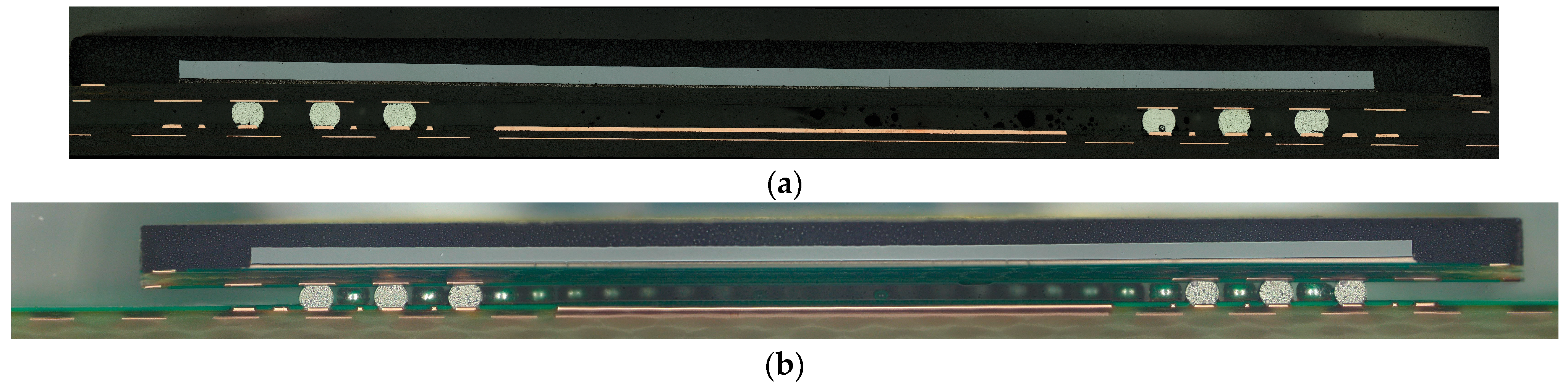
2.1. Test Vehicle Design
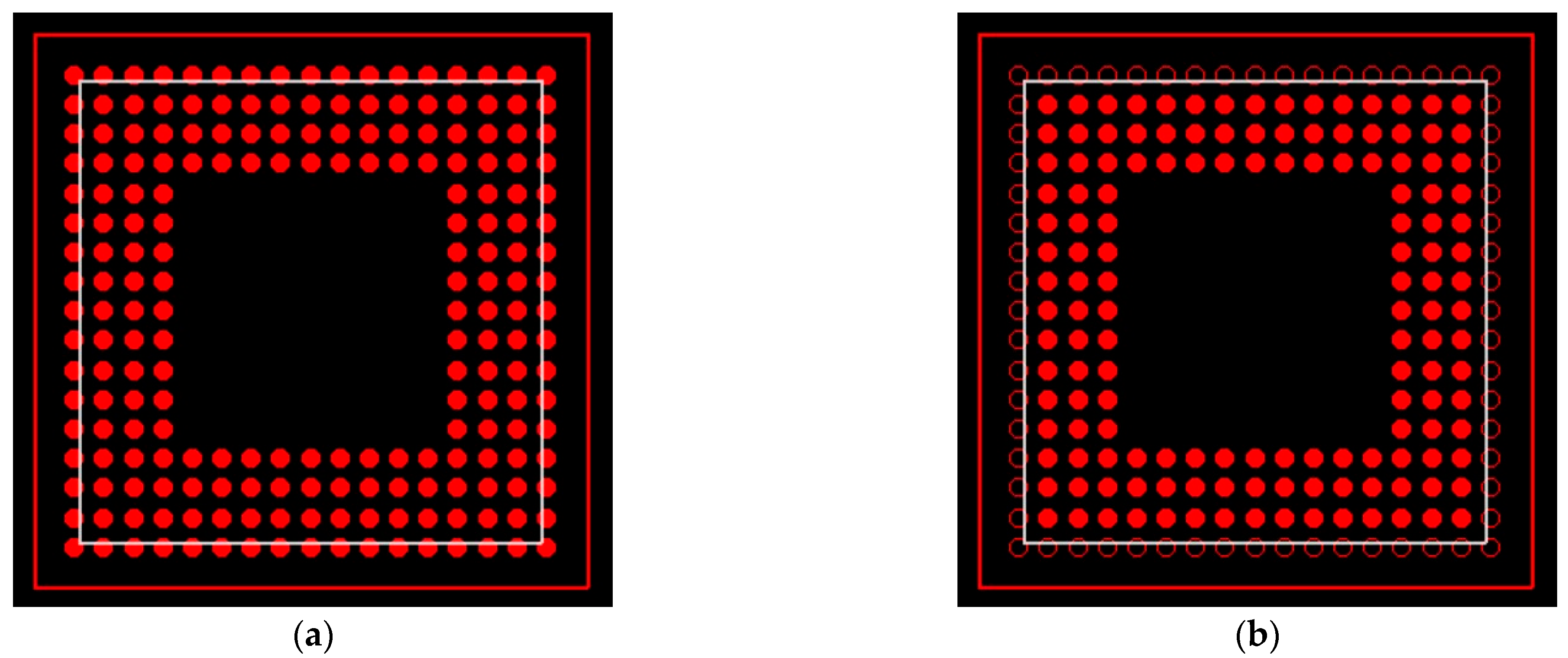
The Amkor CABGA208 component was selected as the test vehicle for this study due to its standard 0.8 mm pitch and four-row perimeter BGA layout, which enables a controlled comparison of different array configurations. This package features a 17 × 17 solder ball array, totaling 208 I/O connections in the 4-Array configuration. The silicon die measures 13 × 13 mm and is centrally located within the 15 × 15 mm package body, spanning only the three innermost rows and columns of solder balls (Figure 1). To evaluate the influence of solder joint placement on reliability, we created two configurations: a conventional 4-Array and a modified 3-Array layout. In the 3-Array design, the outermost rows and columns were omitted, yielding a 144 I/O layout in which all joints are positioned directly beneath the die. This approach eliminates the high-risk peripheral joints—especially prone to early fatigue failures in SAC305—while preserving the original package footprint and die alignment.
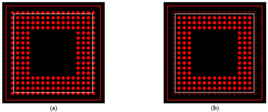
Figure 1.
(a) “4-Array” configuration with all 208 I/O utilized and the (b) “3-Array” configuration with outer row/column joints excluded, resulting in a 144 I/O array.
Unlike prior studies that rely on material changes or process modifications to enhance BGA reliability, this configuration introduces a purely layout-based strategy for reducing thermomechanical risk. By confining all joints within the die footprint, the design directly alters the stress field and failure localization. The present work builds on existing knowledge by systematically evaluating this geometric depopulation method across two solder alloy systems, highlighting the potential of joint layout as a standalone design parameter for improving fatigue performance.
To ensure comprehensive evaluation, we included both SAC305 and Sn37Pb solder alloy configurations in our test matrix, resulting in four distinct test configurations: SAC305 “4-Array”, SAC305 “3-Array”, Sn37Pb “4-Array”, and Sn37Pb “3-Array”.
2.2. Assembly Process
The assembly process followed the methodology established in our previous work [26], ensuring consistency across all test conditions. Bumpless land grid array (LGA) components—based on the Amkor CABGA208 platform—were used as a base to enable controlled attachment of solder spheres. These were attached using a standard no-clean tacky flux (Alpha OM-338), followed by reflow in a forced-convection oven under nitrogen atmosphere to minimize oxidation and ensure uniform wetting. Peaks reflow temperatures were 245 °C for SAC305 and 210 °C for Sn37Pb. No underfill or mechanical reinforcement was applied, allowing the influence of solder joint layout and alloy selection to be isolated.
For the 3-Array configurations, the assembly process remained identical except for the selective omission of outermost joint positions during sphere placement. This allowed fabrication of physically identical components—with identical die, substrate, and package structure—differing only in solder joint population. The same reflow temperature profile and assembly parameters were applied to both 4-Array and 3-Array samples to ensure that any observed reliability differences could be attributed solely to the change in array geometry.
2.3. Accelerated Thermal Cycling
To evaluate solder joint reliability under thermomechanical loading, the assembled test vehicles were subjected to accelerated thermal cycling (ATC). This testing simulates long-term service conditions by inducing cyclic thermal expansion and contraction, which promotes solder joint fatigue. The ATC profile ranged from −40 °C to +125 °C, with dwell times of 10 min at the low temperature and 10 min at the high temperature. Heating and cooling transitions were maintained at an average rate of 10 °C per minute, consistent with JEDEC-standard accelerated cycling protocols [27].
Solder joints were monitored in situ using Analysis Tech STD256 event detectors. These systems were configured to detect resistance loop events exceeding 500 Ω and lasting at least 200 nanoseconds, which reliably indicates the formation of electrical discontinuities associated with joint cracking. This approach enabled accurate logging of the thermal cycle count at which each joint failure occurred, supporting quantitative reliability analysis.
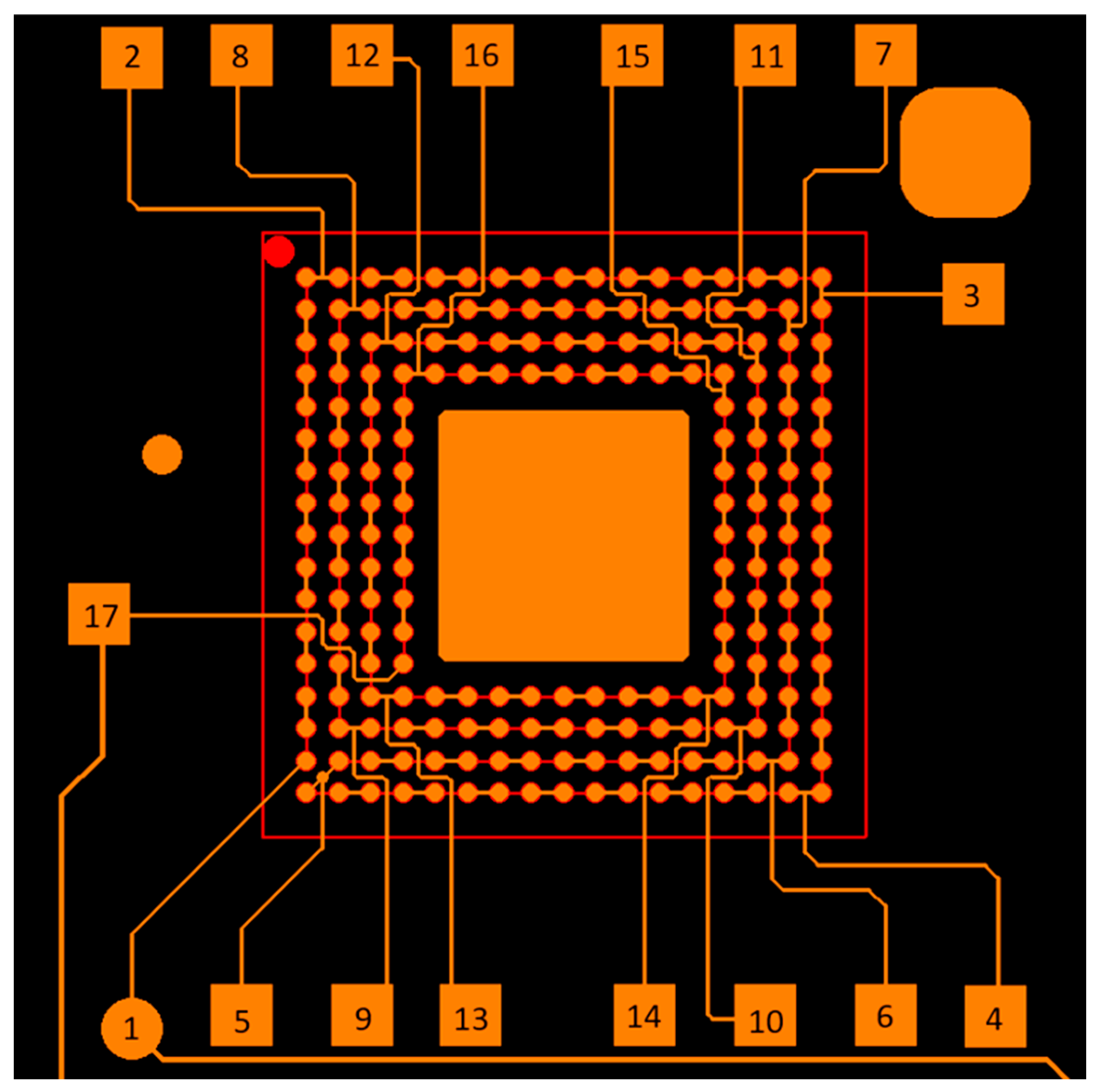
For the 3-Array configuration, a jumper wire was soldered between I/O pad #1 and pad #5 on the PCB to bypass the unpopulated outer-row joints and maintain electrical continuity in the daisy-chained test circuit (Figure 2). This allowed uninterrupted resistance monitoring across the active inner joints without altering the circuit topology. In both 4-Array and 3-Array configurations, the daisy chain was segmented into multiple probe paths to isolate different joint locations. Specifically, probe points 1–5 corresponded to the outermost row (only present in 4-Array), probe points 5–9 captured the second row under the die edge, and probe points 9–17 represented inner joints beneath the die center. This segmentation enabled location-specific failure tracking for each configuration. Each of the four test configurations was evaluated using 15 replicate assemblies.

Figure 2.
Daisy-chain circuit pattern for CABGA208 component and corresponding PCB. Orange color represents PCB pads and traces; red color denotes component outline and internal traces.
2.4. Failure Analysis Techniques
To interpret the failure mechanisms and dominant failure locations associated with each test configuration, a systematic failure analysis approach was employed following thermal cycling. The analysis was conducted in two phases.
In the first phase, electrical continuity across the daisy-chained assemblies was probed using a resistance meter at multiple points on the PCB to isolate the approximate solder joint locations where electrical discontinuities occurred. This allowed for spatial mapping of the initial failure sites across each sample population and provided statistical insight into location-specific failure trends.
The second phase involved destructive analysis through cross-sectioning of selected samples. Standard metallographic preparation procedures—including mounting, grinding, polishing, and etching—were used to prepare the specimens for microscopic inspection. Optical microscopy was then used to examine crack initiation sites, propagation patterns, interfacial separation, and other morphological indicators of failure. Cross-sections were taken along diagonal planes (corner-to-corner) to capture damage distribution and along targeted regions corresponding to electrically identified failure sites. This dual approach provided a full understanding of how failure correlates with solder joint position, array geometry, and proximity to the die.
2.5. Weibull Distribution Analysis
To quantitatively assess and compare the thermal fatigue reliability of each configuration, failure data were analyzed using two-parameter Weibull distribution modeling. For each test configuration, the number of thermal cycles to failure was recorded and fit using maximum likelihood estimation. The resulting Weibull parameters—the shape parameter (β) and the characteristic life (η)—were used to derive additional reliability metrics, including mean time to failure (MTTF) and thermal cycle thresholds corresponding to 1%, 10%, and 50% failure probabilities (t1, t10, t50). These metrics enabled direct, quantitative comparisons between 4- and 3-Array configurations and across the two solder alloys (SAC305 and Sn37Pb).
3. Results
This section presents the thermal cycling test results, Weibull distribution analysis, and failure analysis. The findings are organized to facilitate direct comparisons between the “4-Array” and “3-Array” BGA configurations and to highlight the impact of outer solder joint removal on reliability.
3.1. Thermal Cycling Performance
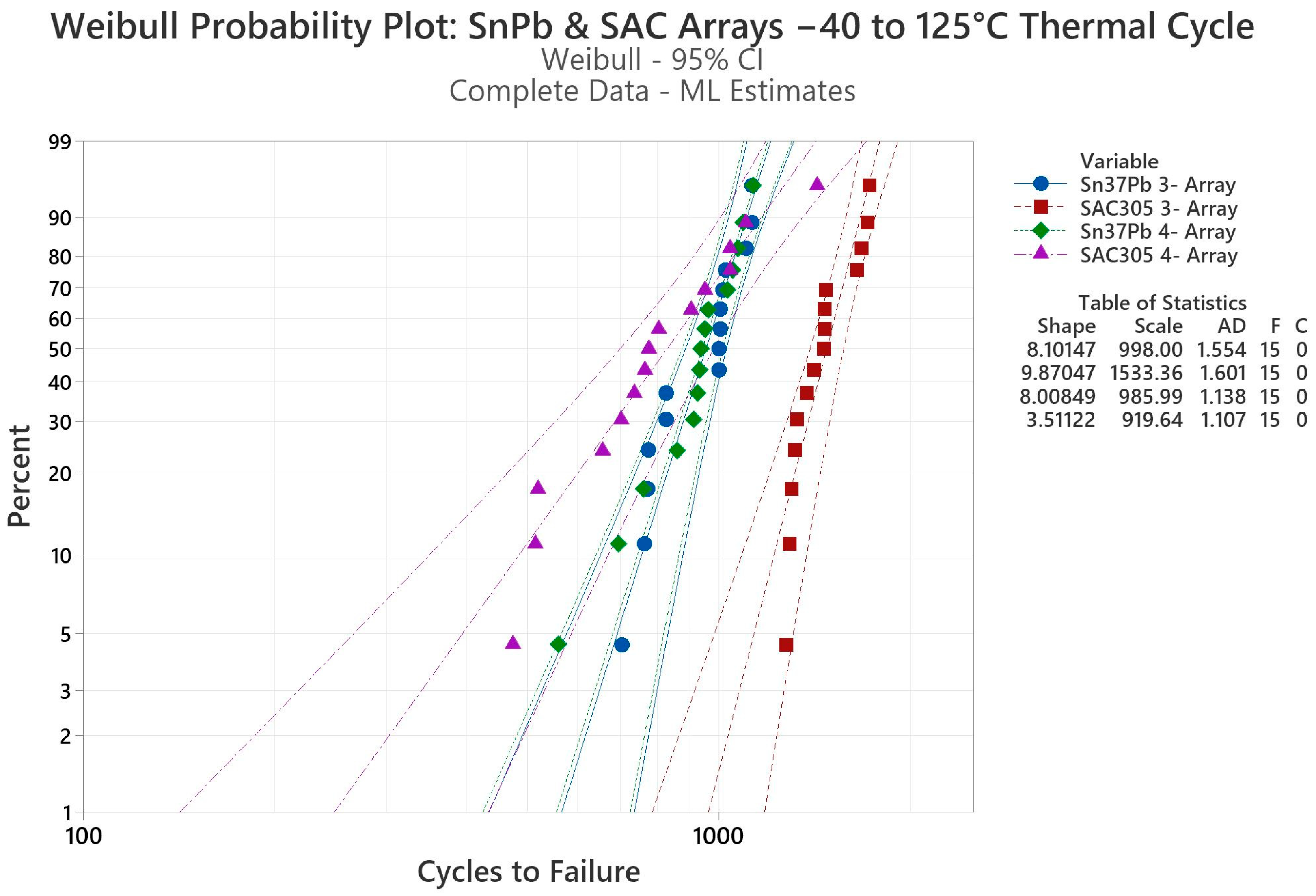
The thermal cycling performance of the four test configurations revealed notable differences in solder joint reliability. Figure 3 presents the corresponding Weibull plots, and Table 1 summarizes the cycles-to-failure data.
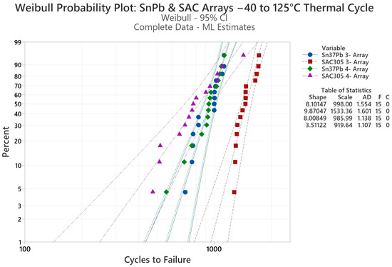
Figure 3.
Weibull plots for CABGA208 configurations subjected to thermal cycling from –40 °C to 125 °C.

Table 1.
Summary of thermal cycling results (−40 °C to 125 °C).
The most prominent observation from the thermal cycling tests was the significant reliability improvement in the SAC305 3-Array configuration compared to the 4-Array. Specifically, the characteristic life (η) of the SAC305 3-Array was 1533 cycles, representing a substantial 1.67× increase over the SAC305 4-Array configuration, which had a characteristic life of 919 cycles. Weibull distribution analysis reinforced this observation, revealing a notably higher shape parameter (β = 9.87 compared to β = 3.51), indicating a more consistent failure mechanism and narrower failure distribution in the 3-Array configurations. Early-life reliability metrics, such as cycles to 1% failure (t1), also showed remarkable improvement, increasing from 248 cycles in the 4-Array to 962 cycles in the 3-Array—a 3.88× enhancement.
In contrast, Sn37Pb configurations showed only a marginal increase in reliability with the 3-Array configuration. The characteristic life increased modestly from 985 cycles for the 4-Array to 998 cycles for the 3-Array configuration, representing a minimal 1.01× improvement. Weibull analysis indicated similar shape parameters (β ≈ 8) for both Sn37Pb configurations, suggesting no substantial shift in failure mechanism consistency. Additionally, the performance distributions for Sn37Pb configurations exhibited significant overlap, reflecting limited benefits from outer joint removal due to persistent shear-dominated failure mechanisms located at internal joints beneath the die edge.
These results collectively demonstrate that perimeter joint removal significantly enhances reliability for SAC305 configurations, primarily by removing the outermost corner joints, which are critical sites of tensile stress-induced failures due to package warpage. Conversely, this strategy provides only limited advantages for Sn37Pb alloys, where critical failures predominantly occur within interior joints.
3.2. Failure Location Analysis
The distribution of failure locations provides critical insight into how outer joint removal influences stress distribution and failure mechanisms in different solder systems. Resistance measurements between multiple probe points on the test board were used to determine the locations of electrical discontinuities across the solder joint array for each configuration.
In the SAC305 4-Array configuration, failures were predominantly concentrated at the corner joints. Specifically, 80% of the failures occurred within probe points 1 to 5, which correspond to the high-stress outermost corner positions. This confirms that warpage-induced mechanical strain remains the dominant failure driver in SAC305 assemblies under thermal cycling conditions. The remaining 20% of failures occurred in the second row (probe points 5–9), where joints are still influenced by warpage but also begin to experience shear stresses due to die edge proximity.
Upon removal of the outer rows and columns in the SAC305 array, the failure pattern shifted significantly. With corner joints eliminated, the new outermost row (probe points 5–9) became the most failure-prone location, accounting for 33% of failures. Additionally, 27% of failures occurred deeper in the array (probe points 9–17), and 40% of samples exhibited multiple simultaneous failure sites. This broader failure distribution reflects a fundamental change in the stress state: removing the dominant corner joints not only significantly reduces the peak stress magnitude (as shown by FEA) but also redistributes the stress more favorably across the remaining joints. This altered stress state, characterized by lower overall stress and a shifted concentration pattern, directly contributes to the observed 1.67x lifetime improvement and explains the shift towards more complex and distributed failure locations throughout the remaining array.
In contrast, the Sn37Pb 4-Array configuration exhibited a significantly different failure profile. Here, 87% of failures occurred in the second row (probe points 5–9), which is located fully beneath the silicon die. These joints are primarily subjected to shear stresses and have been consistently identified as critical failure sites in Sn37Pb assemblies. Only 13% of failures occurred at the corner joints, indicating that warpage-induced stresses play a lesser role in Sn37Pb fatigue failure.
Following outer joint removal, the Sn37Pb configuration retained a similar distribution, with 60% of failures still located in the second row and 27% in inner joints. Only 13% of samples showed multiple concurrent failure sites, highlighting that joint removal had a limited effect on the dominant failure mode in Sn37Pb assemblies. Unlike SAC305, where joint removal significantly altered stress pathways and failure patterns, the behavior of Sn37Pb remained relatively stable due to its inherent failure mechanism being located away from the corners.
These observations are summarized in Table 2, which provides the numerical distribution of failure locations for each configuration.
Table 2.
Distribution of failure locations.
3.3. Failure Mechanism Analysis
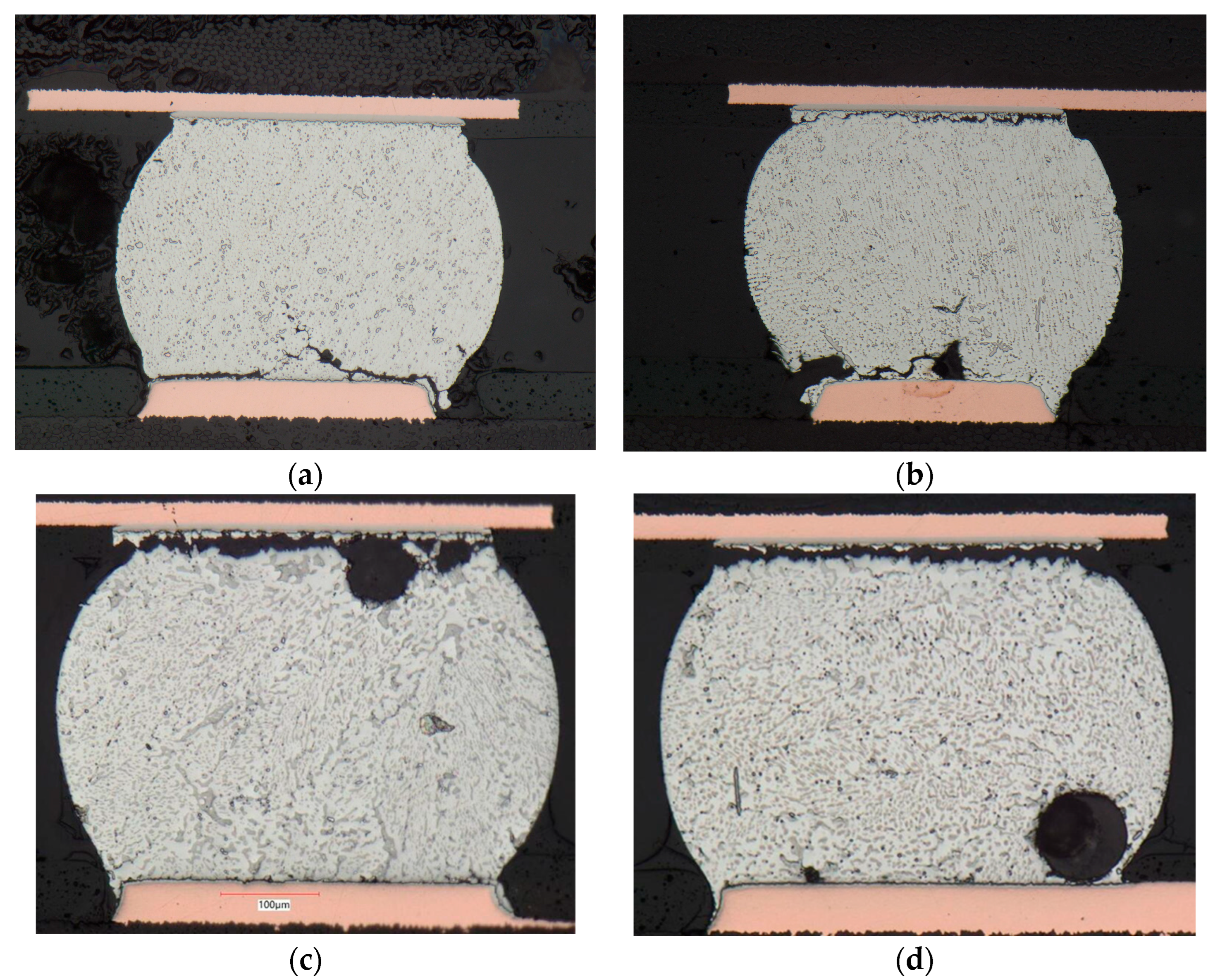
Cross-sectional analysis provided critical insights into the dominant failure mechanisms for each configuration and how outer joint removal influences stress localization and crack propagation paths. Figure 4 illustrates representative diagonal cross-sections of partially populated BGA assemblies, while Figure 5 presents high-magnification images of failed joints from all four test configurations.
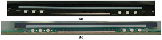
Figure 4.
Diagonal cross-sectional views of BGA assemblies after outer row depopulation: (a) SAC305 solder joints, (b) Sn37Pb solder joints.
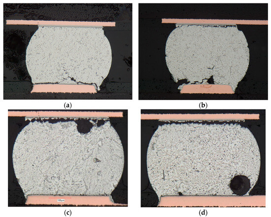
Figure 5.
Cross-sectional images of failed solder joints: (a) 4-Array SAC305, (b) 3-Array SAC305, (c) 4-Array Sn37Pb, and (d) 3-Array Sn37Pb.
In the SAC305 4-Array configuration, failures were consistently observed at corner joints. Cracks initiated near the PCB-side pad and propagated parallel to the board surface, consistent with tensile stresses arising from warpage-induced bending during thermal excursions. These corner locations, subject to the highest mechanical strains due to the distance from the neutral axis and out-of-plane deflection, represented the most critical failure points.
In the SAC305 3-Array configuration, where corner joints were removed, failures shifted inward. Cracks were commonly observed in the new outermost row of joints—located beneath or near the die edge—and appeared on both the component and PCB sides of the joint. This dual-sided crack formation suggests the superposition of shear and tensile stresses, indicating a more complex mixed-mode stress environment. Interestingly, crack paths were less localized and more diffuse compared to the 4-Array configuration. This distributed cracking behavior may explain the improved fatigue life observed, as energy is more evenly dissipated across the joint, effectively reducing local stress intensity.
For the Sn37Pb 4-Array configuration, cracks primarily originated in the second-row joints beneath the die edge, initiating near the component-side pad and propagating parallel to the surface. This failure mode aligns with the expected response of Sn37Pb systems to shear-dominant stresses, which arise from coefficient of thermal expansion (CTE) mismatches between the package and PCB.
The Sn37Pb 3-Array configuration exhibited similar failure behavior. The removal of corner joints did not significantly alter the dominant stress mode or location. However, subtle differences were observed: some joints displayed increased crack branching and secondary crack paths. This suggests a modest redistribution of stresses due to outer joint removal, but without fundamentally altering the failure mechanism. The relatively stable behavior of Sn37Pb in both configurations reinforces the conclusion that its failure is governed more by in-plane shear than out-of-plane warpage effects.
Microstructural examination revealed expected fatigue-related changes across all joints and configurations, including recrystallization, grain coarsening, and interfacial intermetallic compound (IMC) growth. These microstructural features were qualitatively similar in both 4-Array and 3-Arrays, indicating that while stress distributions and crack initiation sites shifted, the underlying material degradation mechanisms remained largely unaffected by outer joint removal.
Overall, this analysis demonstrates that outer joint removal significantly alters the stress distribution in SAC305 assemblies by removing high-risk corner joints, resulting in more balanced stress profiles and increased fatigue life. In contrast, Sn37Pb assemblies remain governed by shear-driven failures at internal joints, with depopulation offering only modest changes in stress state and failure morphology.
4. Finite Element Analysis (FEA)
To investigate the thermo-mechanical behavior behind the experimental results, a three-dimensional (3D) finite element model (FEM) was developed using ANSYS Mechanical APDL. This section presents the FEA approach and results, focusing on the specific modifications made to model the 3-Array configurations.
4.1. Model Description
Building upon the validated methodology detailed in our previous study [26], we developed finite element models for both the “4-Array” (208 I/O) and “3-Array” (144 I/O) configurations investigated experimentally. These models incorporate all key structural components, including the silicon die, package substrate, mold compound (overmold), solder joints, copper pads, and an underlying PCB section.
Quarter-symmetry boundary conditions were applied to reduce computational cost while preserving accuracy, consistent with our prior validation efforts. Displacement constraints were applied to the symmetry planes, as illustrated in Figure 6b, while (c) highlights the exclusion of the outermost solder joints for the 3-Array configuration.
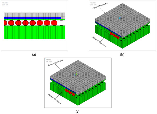
Figure 6.
(a) Side view, (b) oblique view, and (c) quarter-symmetric model of the 3-Array configuration, showing removed outermost solder joint rows.
The Anand viscoplastic model was implemented to accurately capture the nonlinear stress–strain response and creep behavior of solder joints under thermal cycling conditions, an approach extensively validated for solder fatigue analysis. Material parameters for the Anand model were obtained from [28] and are summarized in Table 3. These values were applied consistently across all model configurations to enable comparative analysis of stress evolution between SAC305 and Sn37Pb alloys.
Table 3.
Anand viscoplastic model parameters used in this study for SAC305 (Sn–3.0Ag–0.5Cu) and Sn37Pb eutectic alloys.
4.2. Simulation Approach
The finite element analysis was conducted in two sequential stages. First, the models underwent a simulated solder reflow process, establishing the initial residual stress state within the assemblies after solidification at their respective solder alloy solidification temperatures (217 °C for SAC305 and 183 °C for Sn37Pb). Subsequently, the models were subjected to three complete thermal cycles ranging from –40 °C to 125 °C, matching the experimental accelerated thermal cycling (ATC) conditions. Stress and strain distributions were evaluated throughout these thermal cycles at critical locations to identify maximum stress concentrations and facilitate direct comparison with experimentally observed failure locations.
4.3. Stress Analysis Results
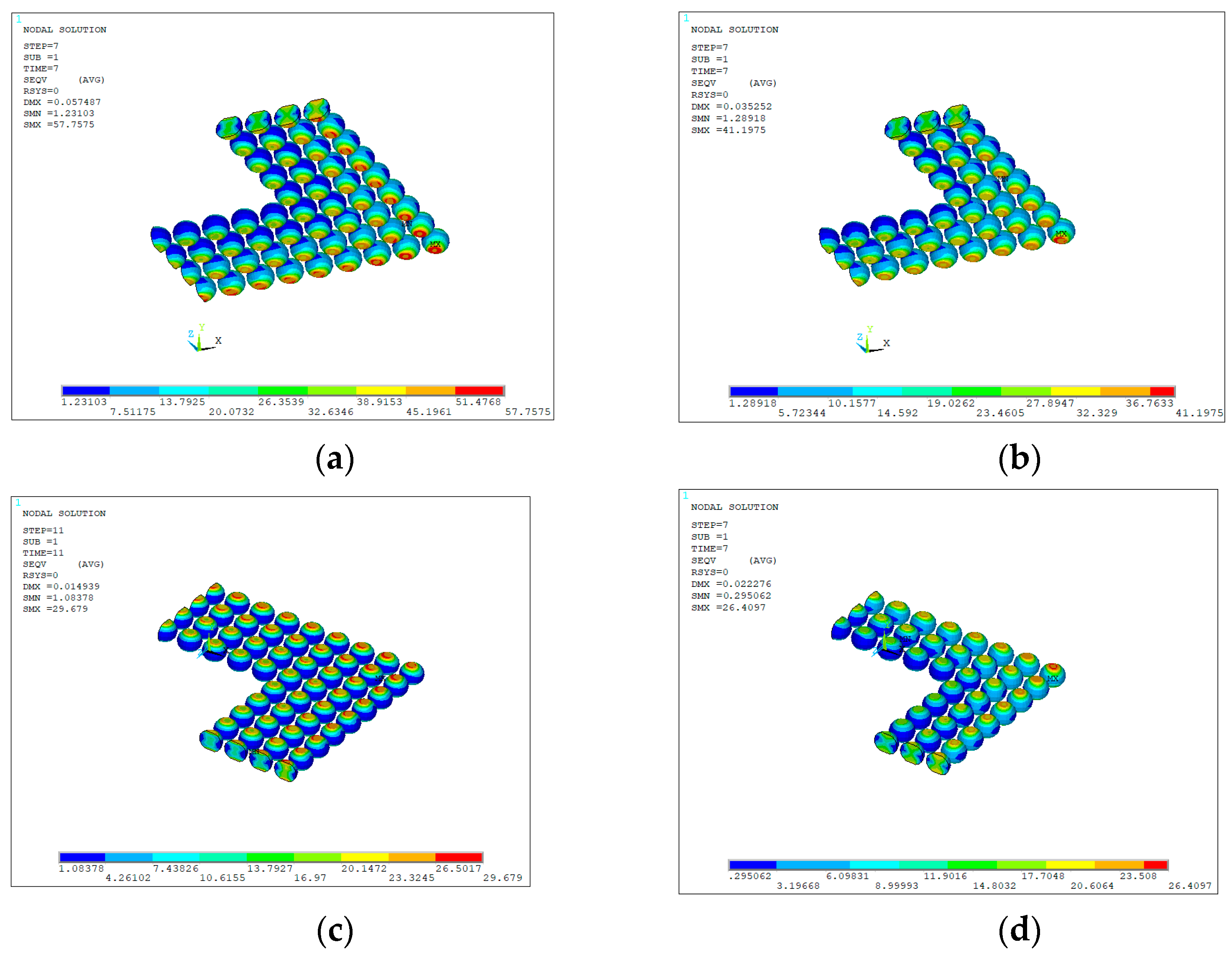
The finite element results revealed significant differences in stress distributions between 4-Array and 3-Array configurations. Figure 7 presents the von Mises stress distributions at the critical stress locations, corresponding to conditions producing maximum thermomechanical stresses.
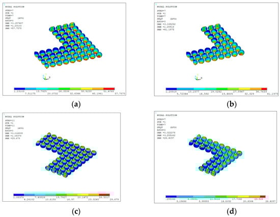
Figure 7.
Von Mises stress distribution. (a) 4-Array SAC305, (b) 3-Array SAC305, (c) 4-Array Sn37Pb, and (d) 3-Array Sn37Pb.
For the 4-Array SAC305 configuration, the maximum von Mises stress (57 MPa) occurred at the corner joints, specifically at the solder-to-PCB interface. This concentration aligns well with experimental results, where 80% of SAC305 failures were observed at these corner locations due to warpage-induced tensile stresses. In contrast, the 3-Array SAC305 configuration exhibited a significantly lower maximum stress of 41 MPa, representing a 29% reduction relative to the 4-Array counterpart. Moreover, stress maxima shifted inward toward the new outermost joint located beneath the die. This redistribution of stresses corresponds to the experimentally observed change in failure pattern, where failures became more distributed across multiple joint locations rather than remaining localized at corner joints.
In the Sn37Pb 4-Array configuration, the maximum von Mises stress was 29 MPa, primarily concentrated at second-row joints directly beneath the die edge, again matching experimental results where 87% of failures occurred at these locations due to shear-dominant loading. Although the 3-Array Sn37Pb configuration showed a significantly lower peak stress (26 MPa, an 11% reduction), experimental data indicated only minimal reliability improvement (1.01×). This apparent discrepancy arises because, despite the reduction in maximum stress magnitude, the primary failure sites (second-row joints) remained unchanged by outer joint removal, maintaining the shear-driven failure mechanism.
Additionally, the FEA identified dual-sided stress concentrations (on both the component and PCB sides) in the new outermost joints of the 3-Array SAC305 configuration. This finding correlates closely with the dual crack formation observed experimentally in cross-sectional analysis, indicating a more balanced stress state compared to the single-sided crack initiation typical in 4-Array configuration.
Overall, these simulation results validate the mechanical hypotheses explaining observed differences in reliability between configurations. They demonstrate that outer joint removal not only reduces the peak stresses but also alters the stress distribution, thus significantly impacting the observed solder joint reliability.
5. Discussion
The finite element and experimental analyses collectively demonstrate that removing the outermost solder joints fundamentally alters stress distributions within BGA assemblies, significantly influencing their reliability. For SAC305 BGAs, the 1.67× increase in mean cycles-to-failure exceeds the improvement expected from merely eliminating mechanically weak corner joints. This suggests that depopulation not only removes vulnerable joints but also promotes a more favorable global stress distribution across the solder array. This interpretation is supported by FEA results, which showed a 29% reduction in peak von Mises stress and a marked shift in stress concentration—from corner joints to positions beneath the silicon die. In contrast, Sn37Pb assemblies exhibited only a marginal reliability gain (1.01×), despite a predicted 11% reduction in peak stress. This discrepancy is attributed to the persistence of shear-dominated stress at second-row joints under the die edge, which are not removed by outer joint depopulation.
These stress redistributions are reflected in the failure mechanisms observed. Cross-sectional analysis revealed that 3-Array SAC305 assemblies developed dual crack fronts at the component-side and PCB-side interfaces of the remaining outer joints. This dual-crack behavior suggests a more balanced and complex stress state compared to the predominantly PCB-side cracking in 4-Array configurations. In contrast, Sn37Pb assemblies showed consistent failure modes across both configurations, supporting the minimal impact of depopulation on their stress response.
The strong correlation between FEA-predicted stress concentrations and experimentally observed failure locations validates the modeling approach, enhancing confidence in the mechanical explanations for the reliability differences identified between configurations and solder alloys.
While the proposed layout strategy enhances thermal fatigue reliability by removing peripheral solder joints, it inherently reduces the total number of available I/Os. In this study, transitioning from a 4-Array (208 I/Os) to a 3-Array (144 I/Os) configuration reflects a 30.8% reduction. This trade-off must be carefully considered in high-speed or high-current applications where signal integrity, power delivery, and routing flexibility are critical. A lower number of ground or power balls may increase IR drop or noise sensitivity.
However, for applications with moderate I/O requirements—such as embedded controllers, sensor modules, or aerospace subsystems—this reduction is often acceptable. These systems typically operate within 100–150 I/O channels and prioritize mechanical robustness under thermal stress. In such cases, aligning all solder joints beneath the die not only improves fatigue reliability but also simplifies routing and enhances package compactness without compromising functional performance.
6. Conclusions
This study investigated the impact of removing outermost solder joints in BGA assemblies subjected to thermal cycling, comparing standard 4-Array and optimized 3-Array configurations for SAC305 and Sn37Pb solder alloys. The experimental results demonstrated that outer joint depopulation significantly enhanced reliability for SAC305, with a 1.67× increase in mean cycles to failure and a nearly fourfold improvement in early-life resistance. In contrast, Sn37Pb assemblies exhibited only marginal gains (1.01×), underscoring fundamental differences in failure mechanisms between the two alloys.
In SAC305 assemblies, depopulation effectively mitigated warpage-induced tensile stresses concentrated at corner joints, resulting in a more balanced stress distribution and dual-sided crack propagation at the remaining edge joints. This was supported by cross-sectional analysis, which revealed a notable shift in failure locations—from 80% corner-dominated in the 4-Array to a broader, more uniform distribution in the 3-Array. Conversely, Sn37Pb failures remained concentrated beneath the die edge, where in-plane shear stresses dominate, indicating that joint removal had little influence on the dominant failure sites. Finite element simulations confirmed these findings, with SAC305 models exhibiting a 29% reduction in peak von Mises stress and a redistribution of critical stress away from the corners.
These results reinforce the value of geometry-driven design interventions in solder joint reliability engineering. By aligning solder joints entirely beneath the silicon die, the 3-Array layout introduces a reliability enhancement mechanism that is independent of material substitution or additional processing steps. This approach is especially attractive for applications with moderate I/O requirements, such as embedded microcontrollers, aerospace subsystems, and automotive sensor modules, where thermal fatigue durability is paramount and layout simplification is desirable.
Nonetheless, the benefits of this layout must be weighed against trade-offs in available I/O count, potential implications for signal integrity and power delivery, and compatibility with system-level electrical requirements. For applications where I/O density is critical, careful electrical co-design may be needed to fully realize the mechanical advantages of joint depopulation.
Looking ahead, future work will focus on extending this strategy to finer-pitch and higher-density BGA packages, evaluating its interaction with underfill materials and encapsulation. Additionally, accelerated testing in more complex thermal and vibrational environments will be conducted to validate its suitability for next-generation high-reliability systems.
Author Contributions
Conceptualization, M.M.; Software, M.A.R. and A.R.; Validation, M.A.R.; Formal analysis, M.A.R.; Investigation, M.A.R.; Writing—original draft, M.A.R.; Writing—review & editing, X.A.C. and A.R.; Supervision, M.M., J.W. and A.R.; Funding acquisition, M.M. and J.W. All authors have read and agreed to the published version of the manuscript.
Funding
This research received no external funding.
Data Availability Statement
The raw data supporting the conclusions of this article will be made available by the authors on request.
Conflicts of Interest
Authors Mohammed Abdel Razzaq, Michael Meilunas, Xian A. Cao and Jim Wilcox were employed by the company Universal Instruments Corporation. Author Abdallah Ramini was employed by the company IBM Corporation.
References
- Refai-Ahmed, G.; Zhirnov, V.V.; Park, S.; Helmy, A.S.; Sammakia, B.; Ghose, K.; Ang, J.A.; Bonilla, G.; Mahdi, T.; Wieser, J.; et al. New Roadmap for Microelectronics: Charting the Semiconductor Industry’s Path Over the Next 5, 10, and 20 Years. In Proceedings of the 2024 IEEE 26th Electronics Packaging Technology Conference (EPTC), Singapore, 3–6 December 2024; pp. 1260–1266. [Google Scholar] [CrossRef]
- Mao, W.; Zhou, Y.; Naik, A.; Sudhakaran, S. Study of BGA Package Cap for High-Performance Computing GPU. In Proceedings of the 2013 IEEE International Symposium on Electromagnetic Compatibility, Denver, CO, USA, 5–9 August 2013; pp. 858–862. [Google Scholar] [CrossRef]
- Stoyanov, S.; Stewart, P.; Bailey, C. Reliability Optimisation and Lifetime Modelling of Micro-BGA Assemblies in Harsh Environment Applications. In Proceedings of the 2021 23rd European Microelectronics and Packaging Conference & Exhibition (EMPC), Gothenburg, Sweden, 13–16 September 2021; pp. 1–8. [Google Scholar] [CrossRef]
- Qi, H.; Osterman, M.; Pecht, M. Design of Experiments for Board-Level Solder Joint Reliability of PBGA Package Under Various Manufacturing and Multiple Environmental Loading Conditions. IEEE Trans. Electron. Packag. Manuf. 2009, 32, 32–40. [Google Scholar] [CrossRef]
- Ghaffarian, R. Accelerated Thermal Cycling and Failure Mechanisms for BGA and CSP Assemblies. J. Electron. Packag. 2000, 122, 335–340. [Google Scholar] [CrossRef]
- Hamasha, S.; Qasaimeh, A.; Jaradat, Y.; Borgesen, P. Correlation Between Solder Joint Fatigue Life and Accumulated Work in Isothermal Cycling. IEEE Trans. Compon. Packag. Manufact. Technol. 2015, 5, 1292–1299. [Google Scholar] [CrossRef]
- Borgesen, P.; Hamasha, S.; Obaidat, M.; Raghavan, V.; Dai, X.; Meilunas, M.; Anselm, M. Solder Joint Reliability under Realistic Service Conditions. Microelectron. Reliab. 2013, 53, 1587–1591. [Google Scholar] [CrossRef]
- Hu, X.; Liu, L.; Liu, S.; Ruan, M.; Chen, Z. Effects of Voids on Thermal Fatigue Reliability of Solder Joints on Inner Rings in Ball Grid Array Packaging by Finite Element Analysis. Micromachines 2023, 14, 588. [Google Scholar] [CrossRef] [PubMed]
- Yu, S.Y.; Kwon, Y.-M.; Kim, J.; Jeong, T.; Choi, S.; Paik, K.-W. Studies on the Thermal Cycling Reliability of BGA System-in-Package (SiP) With an Embedded Die. IEEE Trans. Compon. Packag. Manuf. Technol. 2012, 2, 625–633. [Google Scholar] [CrossRef]
- Wang, H.; Ma, J.; Gong, M.; Su, P. Structural Optimization of Thermal Stresses in BGA Solder Joints Based on Improved BP Neural Network-Genetic Algorithm. Eur. Phys. J. Plus 2023, 138, 712. [Google Scholar] [CrossRef]
- Dilek, S.; Ndip, I.; Rossi, M.; Tschoban, C.; Kuttler, S.; Wittler, O.; Lang, K.-D.; Goetze, C.; Berger, D.; Wieland, M.; et al. Influence of Ball Size and Geometry on the Reliability and RF Performance of mmWave System-in-Package: A Simulation Approach. In Proceedings of the 2021 22nd International Conference on Thermal, Mechanical and Multi-Physics Simulation and Experiments in Microelectronics and Microsystems (EuroSimE), St. Julian, Malta, 19–21 April 2021; pp. 1–4. [Google Scholar] [CrossRef]
- Zhang, T.; Zhu, P.; Lian, J.; Liu, Y. Stress Analysis and Optimization of Pop Package under Random Vibration Loading. IEICE Electron. Express 2023, 20, 20230390. [Google Scholar] [CrossRef]
- Depiver, J.A.; Mallik, S.; Amalu, E.H. Finite Element Comparative Study on Creep and Random Vibrations of Solder Joints in BGA Package. Power Electron. Devices Compon. 2025, 11, 100085. [Google Scholar] [CrossRef]
- Depiver, J.A.; Mallik, S.; Amalu, E.H. Thermal Fatigue Life of Ball Grid Array (BGA) Solder Joints Made from Different Alloy Compositions. Eng. Fail. Anal. 2021, 125, 105447. [Google Scholar] [CrossRef]
- Sun, X.; Li, W.; Chen, M. Influence of the BGA Solder Joint Microstructure on the Thermal Cycling Reliability. In Proceedings of the 2019 20th International Conference on Electronic Packaging Technology (ICEPT), Hong Kong, China, 12–15 August 2019; pp. 1–4. [Google Scholar] [CrossRef]
- Borgesen, P.; Blass, D.; Meilunas, M. Effects of Corner/Edge Bonding and Underfill Properties on the Thermal Cycling Performance of Lead Free Ball Grid Array Assemblies. J. Electron. Packag. 2012, 134, 011010. [Google Scholar] [CrossRef]
- Noh, B.-I.; Lee, B.-Y.; Kim, S.-J.; Jung, S.-B. Evaluation of Thermal Property and Fluidity with Underfill for BGA Package. J. Weld. Join. 2006, 24, 57–63. [Google Scholar]
- Lim, N.R.E.G.; Ubando, A.T.; Gonzaga, J.A. Flip-Chip Package Solder-Underfill Reliability Using Finite Element Analysis. Results Eng. 2024, 24, 103556. [Google Scholar] [CrossRef]
- Tian, G.; Liu, Y.; Johnson, R.W.; Lall, P.; Palmer, M.; Islam, M.N.; Crane, L. Corner Bonding of CSPs: Processing and Reliability. IEEE Trans. Electron. Packag. Manuf. 2005, 28, 231–240. [Google Scholar] [CrossRef]
- Shi, H.; Ueda, T. Thermal Cycling Reliability of Lead-Free Package Stackable Very Thin Fine Pitch Ball Grid Array Assemblies with Reworkable Edge and Corner Bond Adhesives. In Proceedings of the 2011 12th International Conference on Electronic Packaging Technology and High Density Packaging, Shanghai, China, 8–11 August 2011; pp. 1–6. [Google Scholar] [CrossRef]
- Noh, B.-I.; Lee, B.-Y.; Jung, S.-B. Thermal Fatigue Performance of Sn–Ag–Cu Chip-Scale Package with Underfill. Mater. Sci. Eng. A 2008, 483–484, 464–468. [Google Scholar] [CrossRef]
- Serebreni, M.; McCluskey, P.; Hillman, D.; Blattau, N.; Hillman, C. Experimental and Numerical Investigation of Underfill Materials on Thermal Cycle Fatigue of Second Level Solder Interconnects Under Mean Temperature Conditions. In International Electronic Packaging Technical Conference and Exhibition; American Society of Mechanical Engineers: Houston, TX, USA, 2018. [Google Scholar] [CrossRef]
- Hong, J.; Choi, K.; Oh, D.; Park, S.B.; Shao, S.; Wang, H.; Niu, Y.; Pham, V.L. Design Guideline of 2.5D Package with Emphasis on Warpage Control and Thermal Management. In Proceedings of the 2018 IEEE 68th Electronic Components and Technology Conference (ECTC), San Diego, CA, USA, 29 May–1 June 2018; pp. 682–692. [Google Scholar] [CrossRef]
- Chu, L.; Zhou, P.; Shi, J.; Braun, R. Sensitivity Analysis for Geometrical Parameters of BGA in Flip-Chip Packaging Under Random Shear Stress and Thermal Temperature. IEEE Trans. Compon. Packag. Manuf. Technol. 2021, 11, 765–777. [Google Scholar] [CrossRef]
- Lau, C.-S.; Abdullah, M.Z.; Ani, F.C. Effect of Solder Joint Arrangements on BGA Lead-Free Reliability During Cooling Stage of Reflow Soldering Process. IEEE Trans. Compon. Packag. Manuf. Technol. 2012, 2, 2098–2107. [Google Scholar] [CrossRef]
- Razzaq, M.A.; Meilunas, M.; Cao, X.A.; Wilcox, J.; Ramini, A. Effects of Solder Solidification Temperature on Residual Stress Distribution and Failure Location in BGA Solder Joints. Microelectron. Reliab. 2025, 166, 115609. [Google Scholar] [CrossRef]
- “Package Warpage Measurement of Surface-Mount Integrated Circuits at Elevated Temperature|JEDEC.” [Online]. Available online: https://www.jedec.org/standards-documents/docs/jesd-22-b112?destination=node/8107 (accessed on 4 November 2024).
- Zhang, L.; Han, J.; Guo, Y.; He, C. Anand Model and FEM Analysis of SnAgCuZn Lead-Free Solder Joints in Wafer Level Chip Scale Packaging Devices. Microelectron. Reliab. 2014, 54, 281–286. [Google Scholar] [CrossRef]

Disclaimer/Publisher’s Note: The statements, opinions and data contained in all publications are solely those of the individual author(s) and contributor(s) and not of MDPI and/or the editor(s). MDPI and/or the editor(s) disclaim responsibility for any injury to people or property resulting from any ideas, methods, instructions or products referred to in the content. |
© 2025 by the authors. Licensee MDPI, Basel, Switzerland. This article is an open access article distributed under the terms and conditions of the Creative Commons Attribution (CC BY) license (https://creativecommons.org/licenses/by/4.0/).