Article

Design of a High-Gain X-Band Electromagnetic Band Gap Microstrip Patch Antenna for CubeSat Applications

1
Faculty of Engineering, Kyushu Institute of Technology, 1-1 Sensuicho, Tobata Ward, Kitakyushu 804-8550, Fukuoka, Japan
2
IoT Network Innovation Research Center, Kyushu Institute of Technology, 1-1 Sensuicho, Tobata Ward, Kitakyushu 804-8550, Fukuoka, Japan
*
Author to whom correspondence should be addressed.
Electronics 2025, 14(11), 2216; https://doi.org/10.3390/electronics14112216
Submission received: 28 April 2025 / Revised: 23 May 2025 / Accepted: 27 May 2025 / Published: 29 May 2025
(This article belongs to the Section Microwave and Wireless Communications)

Abstract

Microstrip patch antennas (MPAs) are widely used in satellite communication due to their low profile, compact size, and ease of fabrication. This paper presents a design of an X-band microstrip patch antenna using an electromagnetic band gap (EBG) structure for CubeSat applications. The X-band is preferred for CubeSat missions in high-speed communication, long distance or deep space because it allows communication at higher data rates, and the antenna is smaller than those used for lower frequency bands. In our study, the EBG elements are analyzed, modified and optimized so that the antenna can fit a 10 cm × 10 cm surface area of a standard 3U CubeSat structure while providing a significant high gain and circular polarization (CP). A noticeable point of this research is that the simplicity of the antenna and the EBG structure are being maintained by just using a simple single-probe feed to achieve a total antenna efficiency exceeding 90%, and the measured gain of around 11.7 dBi at the desired frequency of 8.483 GHz. Furthermore, the measured axial ratio (AR) is around 1.4 dB at 8.483 GHz, which satisfied the lower-than-3 dB requirement for CP antennas in general. The simulation, analysis and measured results are discussed in detail.

Graphical Abstract

1. Introduction

The CubeSat is one of the most widely used platforms for satellite mission development at the university level, and recently has become a growing sector in the space industry that has a potential to supersede traditional, larger satellites in various applications [1]. CubeSats are well-suited for educational purposes, as well as for testing and demonstrating cutting-edge technologies due to their simplicity, fast time development and significantly lower cost in comparison to the conventional satellite missions. The CubeSats are generally deployed and operate in Low Earth Orbit (LEO) using VHF/UHF, or S-band frequencies for communication. However, recent advancements have demonstrated the potential of CubeSats for high-speed communication, long distance, or even deep space missions by utilizing higher operational frequencies such as the X-band and above [2,3].
Antenna design for CubeSats is a challenging task because of the size and weight limitations of this satellite platform. At VHF and UHF frequencies, wire antennas are predominantly used in LEO CubeSat applications because of their simplicity of design and deployment, their foldability, and the fact that they provide a omnidirectional antenna pattern which is suitable for low-data-rate Telemetry, Tracking and Command (TT&C). However, for higher frequencies such as the S-band, X-band or above, microstrip patch antennas (MPAs) become essential, especially in CubeSat missions that require a higher data rate and more directive communication. At these frequency ranges, due to the shorter wavelength, the size and compactness of the antennas are not as critical as they are in lower frequencies, but the antenna gain becomes a key factor. There are various reported works related to X-band MPAs for CubeSat: Benedikt Byrne et al. [4] designed a compact, optimized circular polarization MPA array for payload Telemetry (TM); this antenna operates at 8.025–8.4 GHz with a measured gain of more than 10 dBi and a measured axial ratio (AR) of lower than 3 dB at 8.212 GHz. However, the design was quite complicated with feeding network and antenna elements on the feed layer, as well as a separate parasitic layer. A high-gain CP planar antenna with a superstrate integrated on top of the antenna radiator was introduced in [5]; the gain is 17 dBic; nevertheless, the feeding network is complicated with four different pins to provide differential signals for CP. Furthermore, the total height of this antenna exceeded the threshold specified in the CubeSat Design Specification (CDS) developed by California Polytechnic State University (Cal Poly) and Stanford University [6]. Even when applying to small satellite standards other than CubeSat, during the launch process, the satellite might experience a strong vibration that leads to a shifting, or even a detaching, of the superstrate and the four supporting standoffs if not mechanically reinforced. In the review article [7], three topologies of low-, medium-, and high-gain X-band MPAs are presented. The medium-gain antenna (MGA) is a 2 × 1 patch array, in which a dual-feed network is applied for each element to create CP. This MGA reached a gain value of 9 dBi and fits well in a surface area of 2U (10 cm × 20 cm). It is clear that in the above MPA designs, an array of elements or auxiliary components for the antenna radiator must be implemented to achieve good gain. Moreover, a feed network must also be used to create circular polarization, that can lead to additional insertion losses, phase imbalance issues, and fabrication complexity.
The purpose of the present paper is to introduce a novel CubeSat microstrip patch antenna design that balances high gain, circular polarization, simplicity and robustness. The method of integrating an electromagnetic band gap (EBG) into the MPA is considered. The EBG structures belong to a specialized class of metamaterials that are composed of artificial periodic cells, which are being designed to either stop or allow the propagation of electromagnetic waves within a specific frequency range, thus effectively improving the antenna performance. A variety of EBG research works for MPA gain enhancement are recorded, for instance, using elliptical surrounding holes lattice EBG [8], combining EBG together with defected ground [9] or fractalizing the EBG elements [10], implementing an EBG superstrate with the aperture feed MPA [11], or inserting an EBG ring to act as a secondary ground plane between the MPA radiator and the normal ground [12].
In our study, the mushroom-like EBG type is chosen. The EBG elements are positioned to form only one ring outside a single-element MPA radiator. The optimization of the EBG ring shape and the distance from the EBG elements to the central MPA radiator, as well as the simplified design of both the EBG structure and the antenna single-probe feed to apply to the CubeSat platform are the novelties of our research compared to the aforementioned studies. Furthermore, the central MPA radiator can be simply modified by adding square-shaped slots symmetrically along the diagonal directions [13] to produce circular polarization without being affected by the outer EBG ring.
This paper consists of five parts. The first part is the above introduction, the second part presents the principle of the EBG and explains its effect on the antenna gain enhancement. The third part demonstrates the antenna design and simulation process, from the original antenna to the antenna after adding the EBG and modifying the radiator to create circular polarization. The simulations are carried out while taking the effect of the CubeSat platform into account. The antenna parameter study is also presented in this section. The fourth part describes the antenna measurement and analyses of the measured results. The final part includes the discussion and the details of our future work.

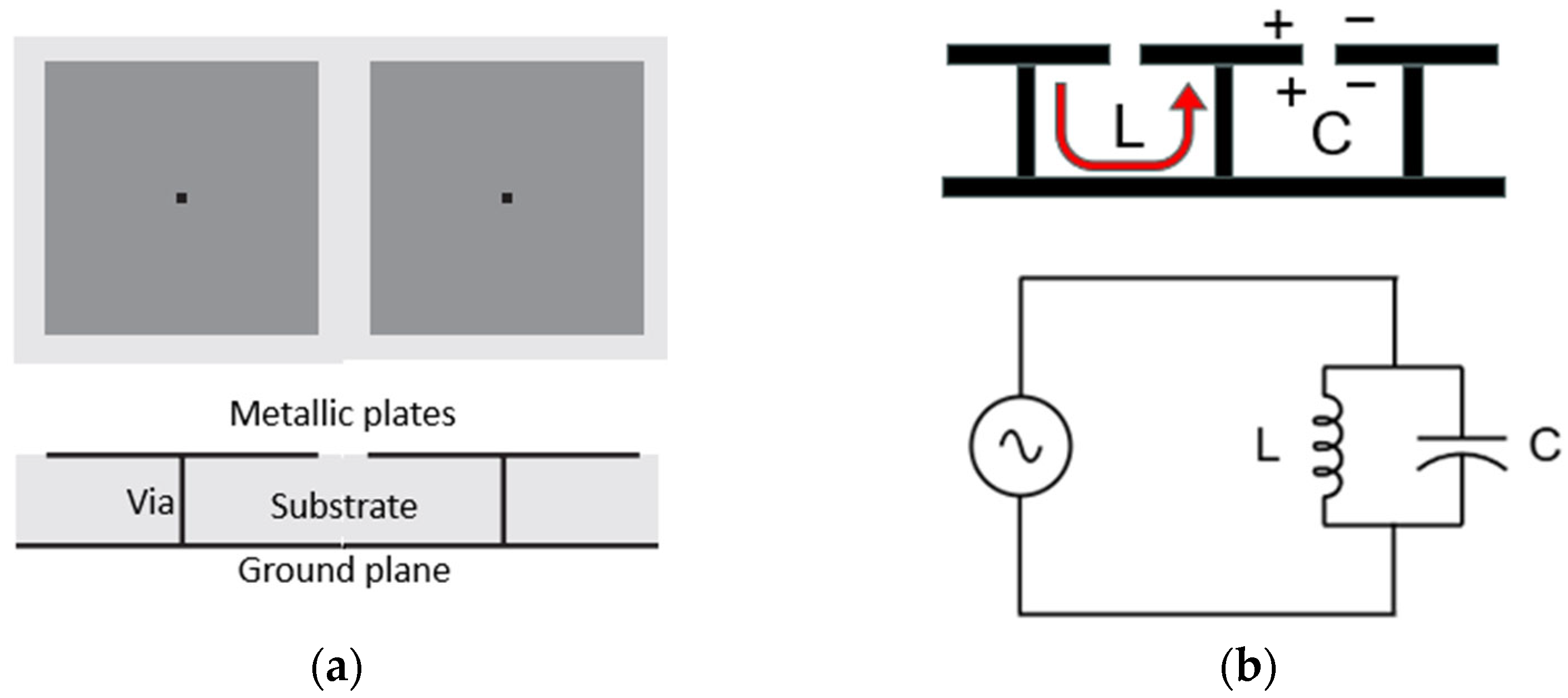
2. EBG for Microstrip Patch Antenna

The previous section provides a general definition of the electromagnetic band gap (EBG), which originates from the photonic band gap (PBG) phenomenon observed in optics [14], and the term ‘EBG’ was introduced in [15]. There are various types of EBGs but they are generally classified into three main groups: (1) 1D transmission lines, (2) 2D planar surfaces and (3) 3D volumetric structures [16]. Our study focuses on the 2D planar surfaces EBG group, specifically the mushroom-like EBG structure, which was first introduced in 1999 by Dan Sievenpiper et al. [17]. This structure consists of a ground plane, a dielectric substrate on which metallic plates are mounted, and metallic vias to connect these plates through the substrate to the ground. The operation mechanism of the mushroom-like EBG structure can be explained by referring to an equivalent parallel resonant LC circuit, as described in Figure 1.
As can be seen from Figure 1a, two adjacent metallic plates have connecting vias (denoted as black dots in the top view) to the ground plane. The gap between the plates can be considered as a capacitive component, while the vias provide inductive paths to the ground plane. In Figure 1b, when the EBG structure interacts with the electromagnetic wave, a voltage applied along the top surface leads to an accumulation of charges at the edges of the plates, thus forming a capacitance. As the charges travel back and forth between the metallic plates and the ground plane through the inductive paths created by the vias, an inductance is created [18]. The bandgap formation can be explained by considering the resonance of the parallel LC circuit at a specific frequency, where a stopband is created and prevents the surface waves from propagating. The values of L and C can be varied by modifying the physical dimensions such as the size of the EBG elements, the gap between them, the length of the ground connecting vias, as well as the dielectric constant of the substrate. Therefore, the frequency band gap of the structure can be tuned. In further detail, larger EBG element dimensions increase the capacitance, and smaller gaps enhance the interactions of the capacitive components, leading to a decrease in the bandgap frequency. Meanwhile, increasing the via lengths will cause a higher inductance which reduces the bandgap frequency. Furthermore, when increasing the dielectric substrate thickness, enhanced fringing fields improve the antenna radiation efficiency that leads to a higher gain. However, excessive thickness can cause stronger surface wave propagation, which deteriorates the radiation performance.
The advantages of the mushroom-like type over other EBG types are the good band gap performance, compact design, and the ease of fabrication and integration on printed circuit boards (PCBs), making it a good candidate for planar and microstrip patch antenna applications. The mushroom-like EBG can be applied to single-element MPAs [9,10,19,20,21,22,23], as well as MPAs in an array configuration [24,25,26,27]. Figure 2 shows two examples of the deployment of mushroom-like EBG structures for these two cases. The enhancement of antenna gain and radiation efficiency due to surface wave suppression can be explained for these two cases as follows: For the single-element MPA, the surface waves travel along the substrate and radiate from the edges of the antenna, contributing to the unwanted edge radiation that degrades the antenna efficiency. By filling up the non-metal space from the center radiator to the edges of the MPA by EBG elements, stopband ‘rings’ are created and prevent the surface wave from going beyond the patch area. Consequently, the edge diffraction that leads to unwanted edge radiation will be minimized. This conclusion is further reinforced by the demonstrated cases of a PBG, the structure from which the EBG is derived [28,29,30]. For the MPA array, the mechanism is the same as that of the single-element MPA: When separating the antenna elements using mushroom-type EBGs, stopband ‘trenches’ are created and the mutual coupling caused by surface wave between them will be decreased. Therefore, the antenna gain and performance will be boosted in both cases.

3. Antenna Design and Parameters Study

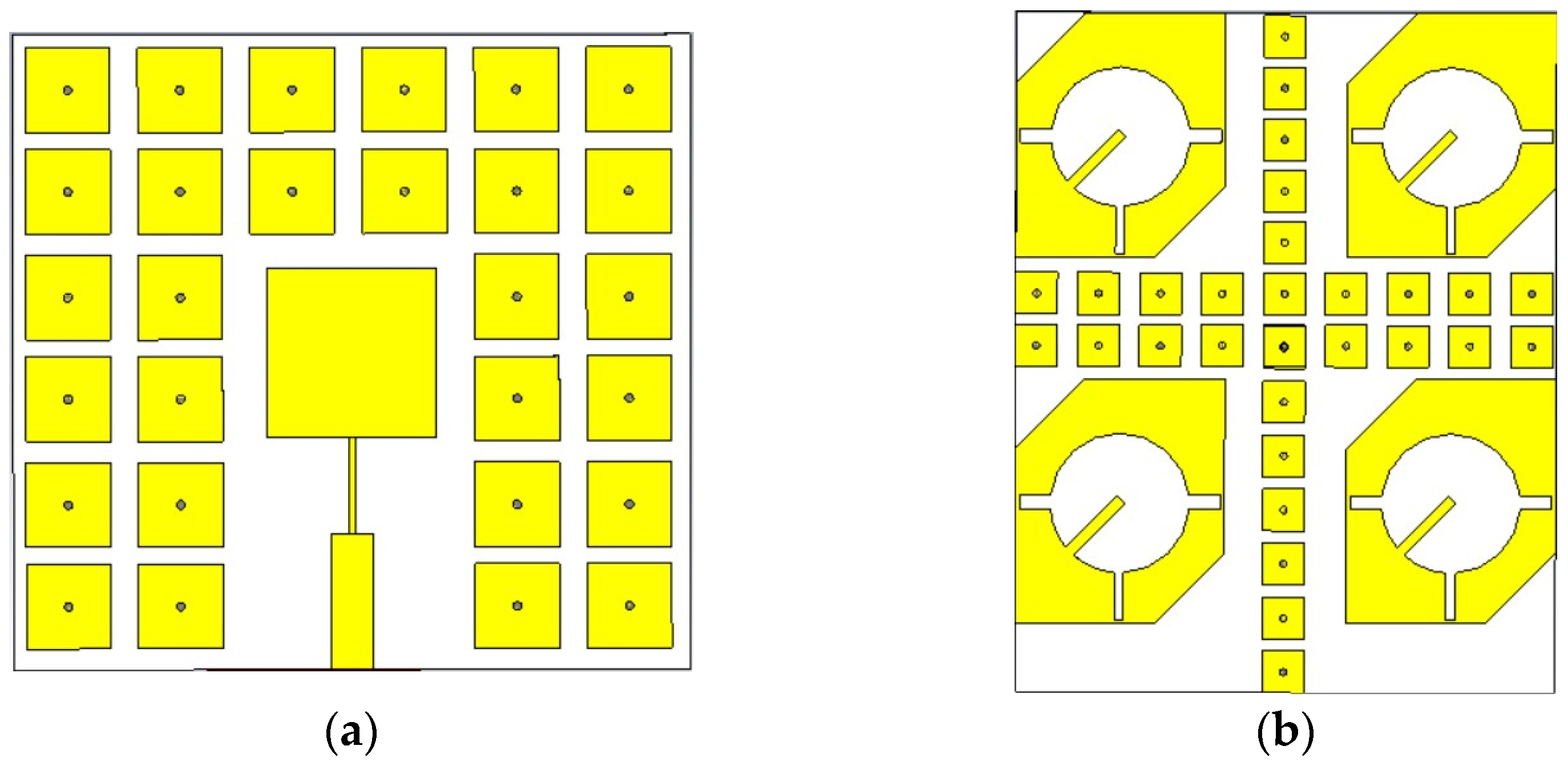
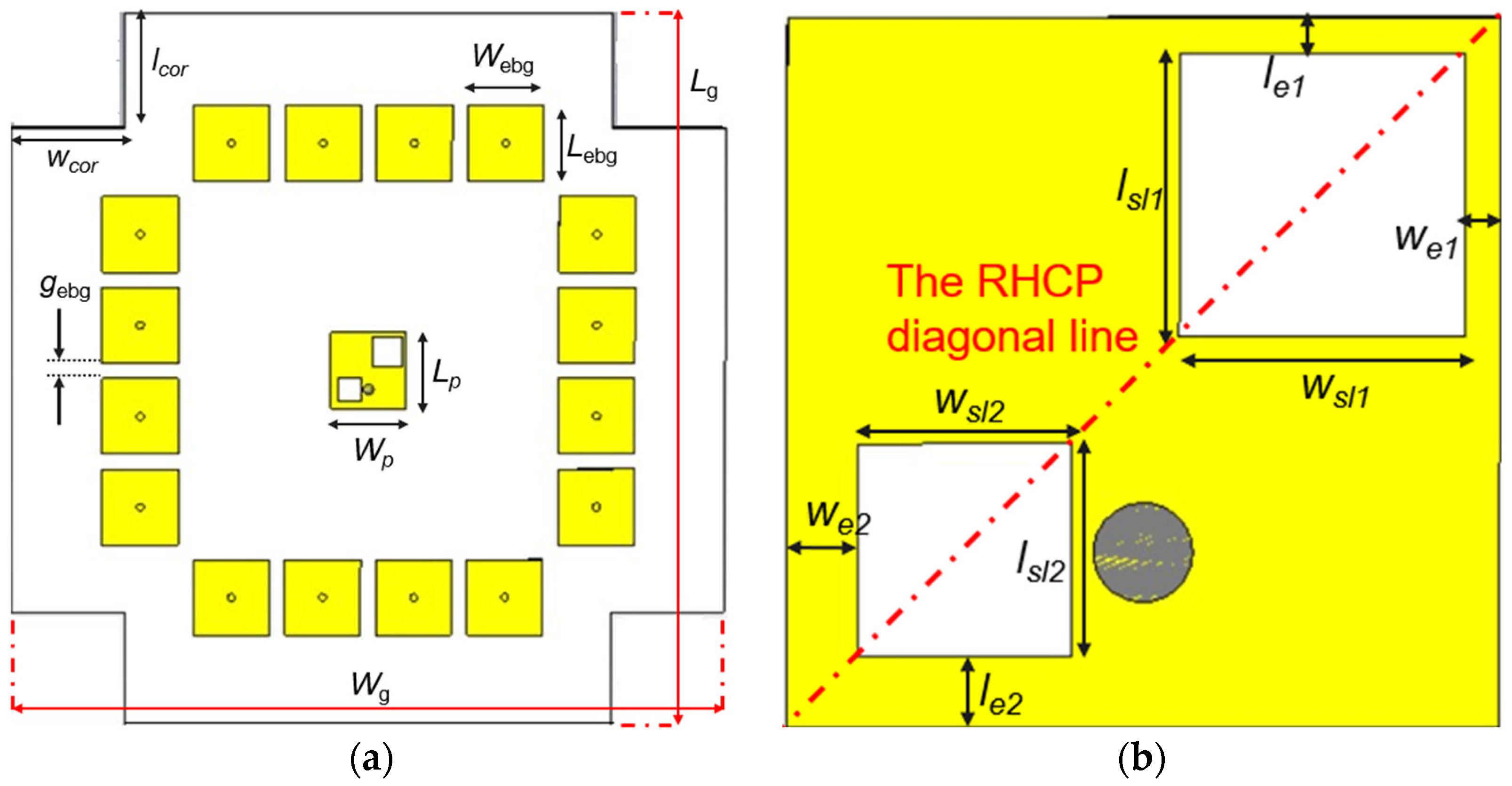
3.1. Design and Simulation of the EBG MPAs

As suggested in [23], the band-gap performance is improved as the number of EBG rings increases. However, when applying the mushroom-like EBG ring structure to the CubeSat platform, we will face the challenge of surface area limitation. It will be difficult to design two or more EBG rings with reasonable spacing around the MPA for the EBG structure to be effective. Therefore, practically for CubeSat MPA designs in the X-band and below, the number of EBG rings should only be one when applying to the 10 cm × 10 cm surface area. However, not all of that area can be used for antenna mounting, because the four outer corners of the surface are the protruding terminals of the four main rails, where the satellite’s deployment switches can be mounted for CubeSats to use the Poly Picosatellite Orbital Deployer (P-POD) launcher tube [31,32]. Furthermore, according to the CDS of Cal Poly, the total height of the antenna structure must not exceed 6.5 mm in the direction normal to the surface from the plane of the rails [6]. This constraint ensures compatibility with the P-POD deployment system and prevents interference with adjacent payloads during the launch. However, this is a stringent condition that limits many attractive high-gain antenna designs, such as multiple EBG layers, metamaterial superstrates, or the Frequency Selective Surface (FSS), being applied to CubeSat. Our single-layer EBG antenna design offers a viable solution that can compromise between these CubeSat requirements and the antenna performance.
Figure 3 illustrates the primary structure of a 1U CubeSat with protruding rails and the available surface area (colored in blue) on which the antenna can be mounted on the ±Z side. This figure also shows the unavailable areas in which the rails are located (colored in red). The metallic and non-metallic parts of the antenna are indicated in yellow and white, respectively. Our proposed X-band EBG MPAs for circular polarization (CP) are designed as shown in Figure 4. The antenna includes an outer ring of 16 mushroom-like EBG elements, which surround the main patch radiator at the center; these components are located on the top layer of the antenna and are all made of copper. Each EBG element has a connecting via at the center that connects them through the dielectric substrate to a normal copper ground layer. The dielectric substrate is Rogers RT5880 which has the thickness h = 1.6 mm and the permittivity ε = 2.2. The gaps between the EBG elements and the presence of these connecting vias form the L and C components of the mushroom EBG structure, as explained above. When the EBG elements are arranged periodically in a ring around the center patch radiator, a composite surface with a frequency-selective bandgap behavior is created. Furthermore, the EBG ring modifies the local effective permittivity and permeability in the areas where it is present, resulting in the suppression of the surface wave propagation. Therefore, the metamaterial characteristics of the antenna structure have been created.
Each EBG element has the dimensions of 10 mm × 10 mm, which is the same as that of the center patch radiator, and the spacing between two adjacent EBG elements is 2 mm. The four outer corners of the antenna are cut off to allow it to be mounted on the CubeSat surface without touching the rails, and each cut-out square is 15 mm × 15 mm in size. Though the EBG ring is the main factor in increasing the antenna gain, these truncated corners also contribute to this increment, as will be discussed later. The input impedance of the antennas is 50 Ohms, and the center square patch is fed by a single-probe feed using an SMA connector from the antenna ground plane.
In Figure 4b, two square-shaped slots are etched along the right diagonal line of the center patch to create Right Hand Circular Polarization (RHCP), which is similar to one of the structures introduced in [13]. By embedding these slots like this, the antenna’s current distribution is perturbed, leading to the excitation of two orthogonal resonant modes with the same amplitude but with a 90-degree phase difference, which is necessary to produce circular polarization. The placement and dimensions ratio of the square slots, as well as the location of the probe feed are optimized to reach good circularly polarized radiation.
The minimum antenna design requirements are tabulated in Table 1. These requirements are for maintaining a data rate of 10 Msps when using a QPSK modulated signal for our CubeSat’s X-band transmitter module.
The antennas are simulated and optimized using CST Studio Suite 2019 software. The Time-domain solver is used for full-wave electromagnetic simulations. The antenna design procedure is summarized as follows:
  • Design and simulate the original CP MPA in the available surface area with only the center radiator, at the target frequency of 8.483 GHz;
  • Design and simulate the MPA with the mushroom-like EBG structure added;
  • Optimize the related parameters to satisfy the requirements of gain and CP.
The parameters of the CP EBG MPA are listed in Table 2. The units are millimeters.
The important antenna parameters such as the input reflection coefficient (S11), antenna gain (S21), and the antenna far-field radiation pattern are simulated. In addition, simulation of the axial ratio (AR) at the operating frequency of 8.483 GHz and the 3 dB axial ratio bandwidth (ARBW) over frequencies will be carried out to evaluate the circular polarization quality of the antenna. Figure 5 shows the simulated S11 values of the original MPA and the CP EBG MPA. At 8.483 GHz, the S11 values of the original MPA and the CP EBG MPA are −21.9 dB and −18.2 dB, respectively. However, it is evident in Figure 5 that the circular polarization antenna has the better −10 dB operation bandwidth, which is around 0.7 GHz in comparison to the −10 dB bandwidth value of 0.47 GHz of the original antenna.
The gains over frequencies of these antennas are presented In Figure 6. From this figure, we can see that the gains at 8.483 GHz of the original and the CP EBG MPAs are, in turn, 8.27 dBi and 11.72 dBi. This means that a gain increment of around 3.5 dB is achieved after adding the mushroom-like EBG ring to the original antenna structure.
Figure 7 depicts the normalized far-field antenna radiation patterns of the original and the EBG antennas in polar coordinates. The real values of the main lobe magnitude were mentioned under the drawings. As observable in Figure 7a,b, the shape of the CP EBG antenna radiation pattern is more directive than that of the original MPA, with the 3 dB half-power beamwidth (HPBW) value of 28.9°. The surface current distribution over time of the antenna before and after adding the EBG is demonstrated in Figure 8. It is apparent from this figure that at the phase of ωt = 90°, the near-field level at the lower edge of the original MPA is 1 A/m while that value at the same position of the CP EBG MPA is 0.2 A/m, which corresponds to the dB-scale values of 0 dB and −14 dB. The formula to convert the values from A/m to the dB scale is as follows:
E d B = 20 l o g 10 E
This means that there is a surface wave suppression at the antenna edges and the unwanted edge radiation is significantly reduced by approximately 14 dB. As a result, more energy is directed into the main radiation beam, therefore improving the antenna gain.
The axial ratio over frequencies of the CP EBG MPA are presented in Figure 9. As depicted in this figure, the AR at 8.483 GHz is around 1.6 dB, which is below the 3 dB threshold value for a CP antenna. The 3 dB ARBW is around 190 MHz, from 8.34 to 8.53 GHz.

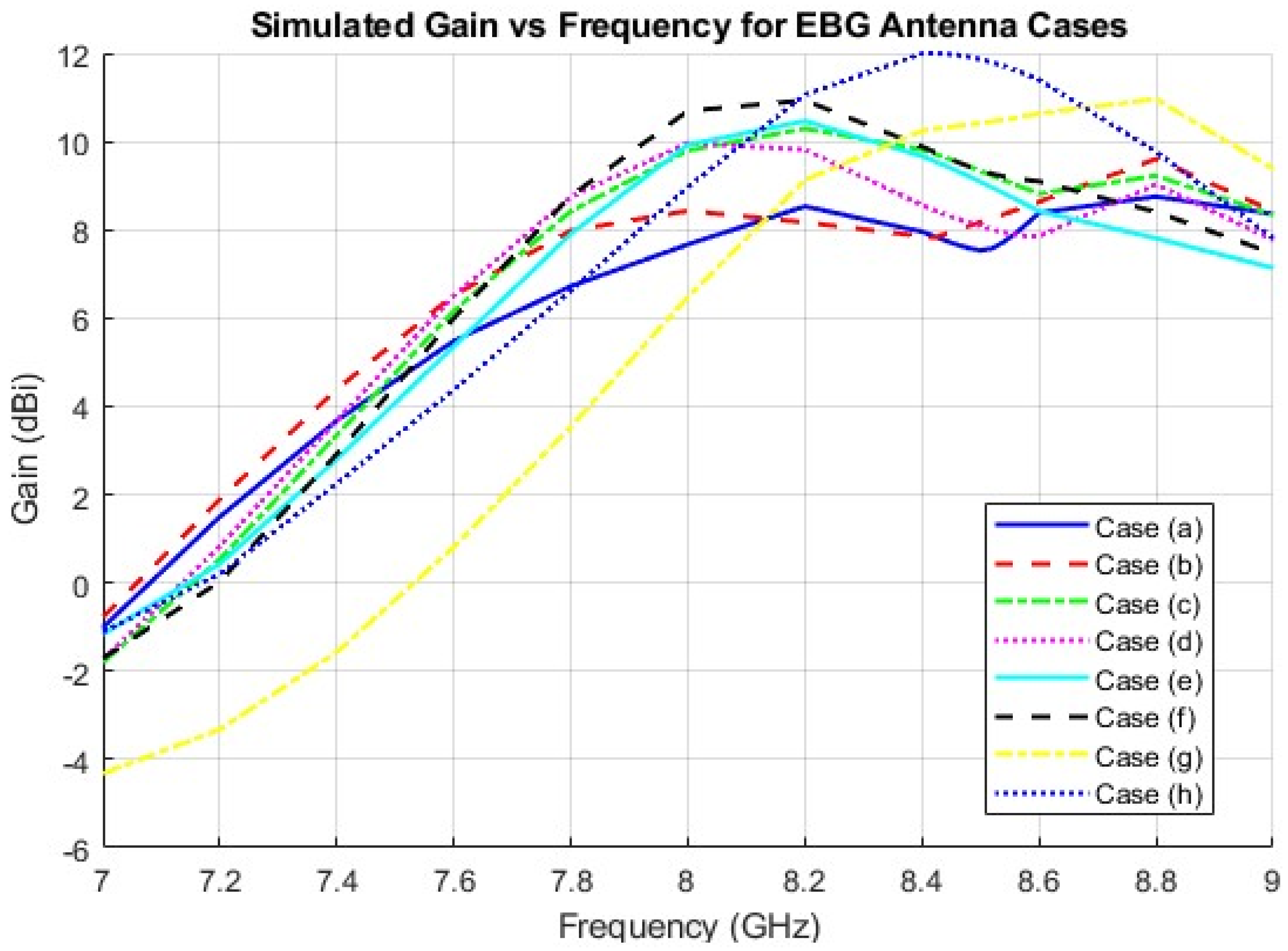
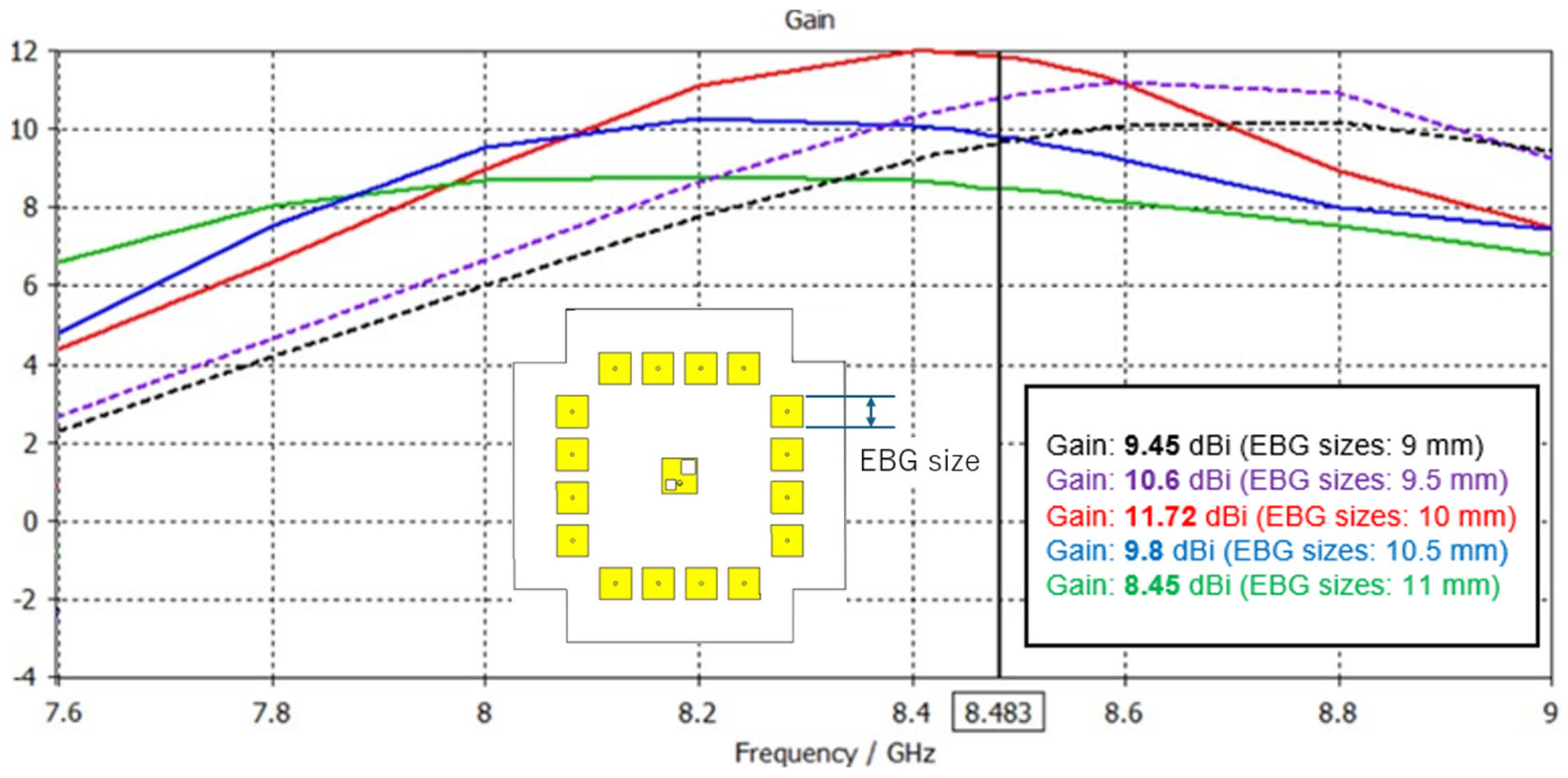
3.2. Parameters Study

This section discusses the influence on the antenna gain enhancement of the design parameters such as the shape and number of the EBG structures, as well as the size of the mushroom-like EBG elements. Each parameter will be varied separately while the other parameters remain unchanged to emphasize its effect on the antenna gain. Firstly, the effect of the EBG shape is considered. Figure 10 demonstrates the EBG ring configurations that we have designed simulated, and the distance from the center radiator to its nearest EBG elements is the same in all the configurations, which are labeled from Case (a) to Case (h). Figure 10a shows the original structure (Case (a)), which is a full two-layer EBG ring with the total number of 48 mushroom-like EBG elements. Apparently, this structure is not applicable to the 3U satellite model without modification, as explained in Section 3.1. As can be seen from Figure 10b–h, we gradually removed the outer-layer EBG elements, relocated some elements, and altered the structure of the inner-layer EBG elements until we found the optimal configuration. The effect of this structure alteration is shown in the increase in the antenna gains as depicted in Figure 11. In this figure, at 8.483 GHz, we can see that the gain of Case (a) is around 7.6 dBi, which is even lower than before adding the EBG, but in Case (c), after removing 25 EBG elements of the outer layer, the gain is boosted to 9.4 dBi. In Case (f), we only keep two EBG elements of the outer ring and in Case (g), the outside EBG ring is totally removed, and the gain values continue to rise to approximately 10.9 dBi. However, the peaked gains in these cases are still not located at 8.483 GHz. Finally, in Case (h), the truncation at the four outer corners of the antenna resulted in a further gain increase of around 0.8 dB to reach the highest value of 11.72 dBi exactly at the target frequency 8.483 GHz. This can be explained as follows: By truncating the four corners, the surface wave, as well as the diffraction and scattering waves on these areas will be removed. Moreover, this leads to a shift in the bandgap center frequency, nudging it to align with the antenna target frequency. Consequently, more power is radiated into free space, leading to an improvement in the antenna gain. Therefore, cutting the four edge corners is not only structurally necessary to fit the antenna on the CubeSat surface, but also provides good electromagnetic effects in terms of gain enhancement and frequency tuning.
Secondly, the effect on the gain enhancement when changing the dimensions of the EBG is studied. In this case, we use the Case (h) EBG configuration in Figure 10h. Only the dimensions of the EBG elements are varied while all other parameters remain unchanged. The length and width values are equal to ensure that each EBG element is always square with the ground via located in the center of the element. It is important in maintaining the rotational symmetry of the mushroom EBG elements, as well as the antenna structure, to guarantee polarization-independent reflection phase characteristics that are required for our CubeSat antenna application. Figure 12 illustrates the gain values when changing the EBG dimensions from 9 mm to 11 mm with a step size of 0.5 mm. As shown in this figure, the highest gain of 11.72 dBi at 8.483 GHz (denoted as the solid red line) is reached when the dimensions of the EBG elements are 10 mm, which is the same value as the size of the square center patch radiator. Deviations from this optimal size shift the bandgap away from the target operation frequency and reduce its effectiveness, leading to a decline in the antenna gain.

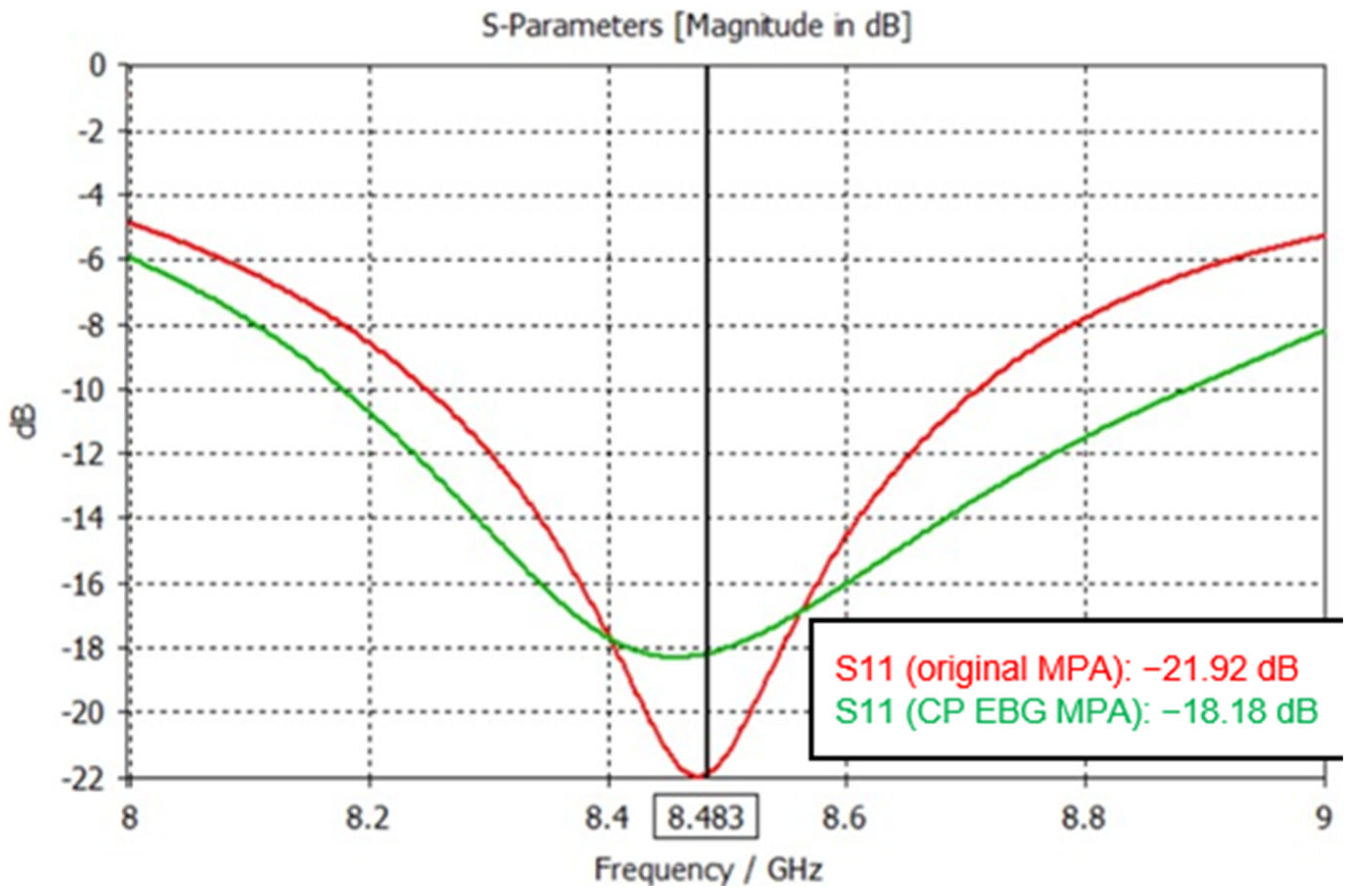
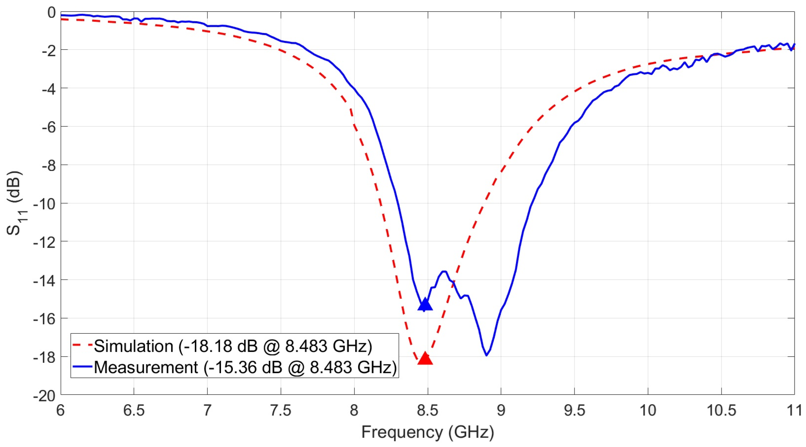
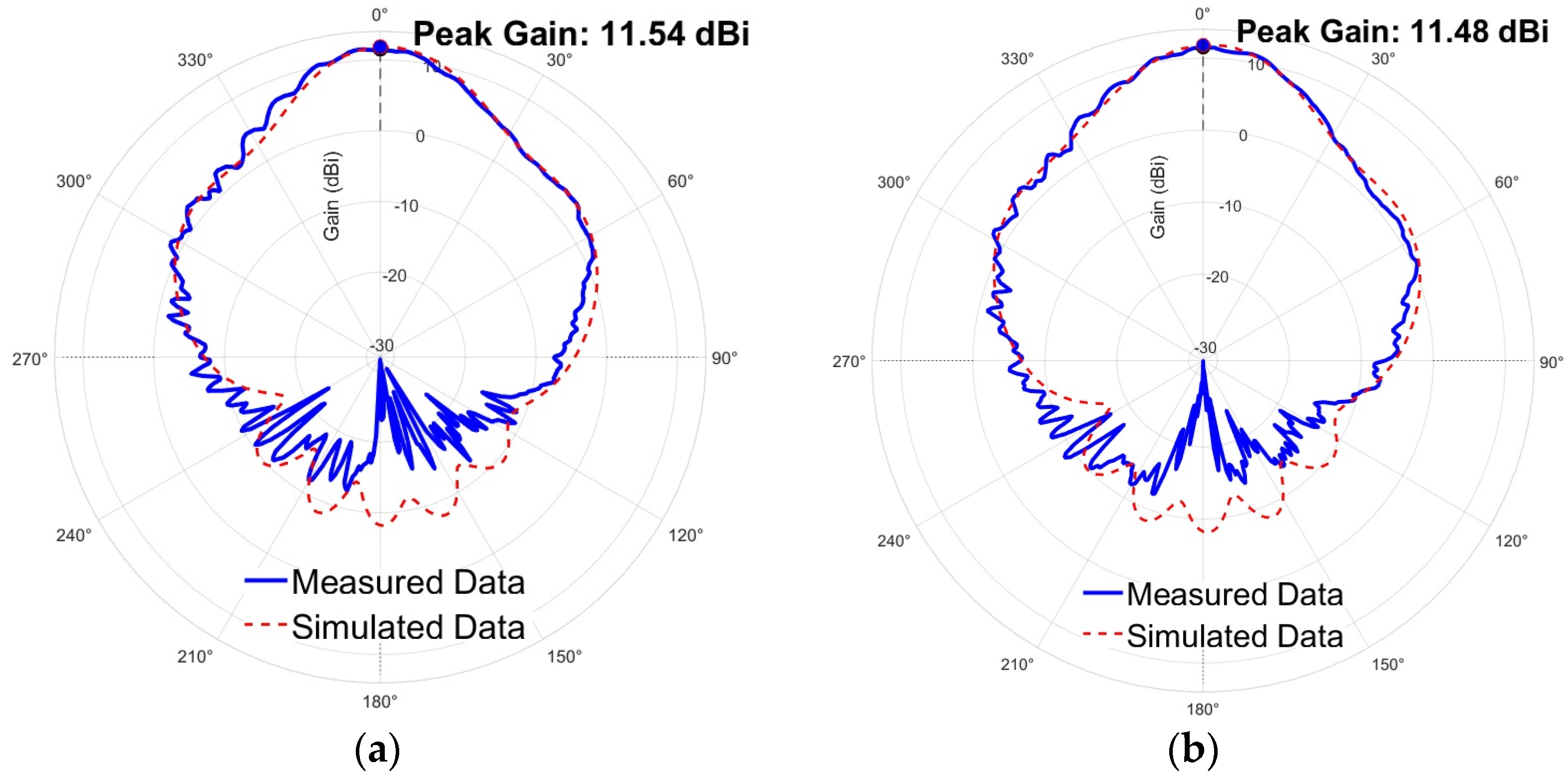
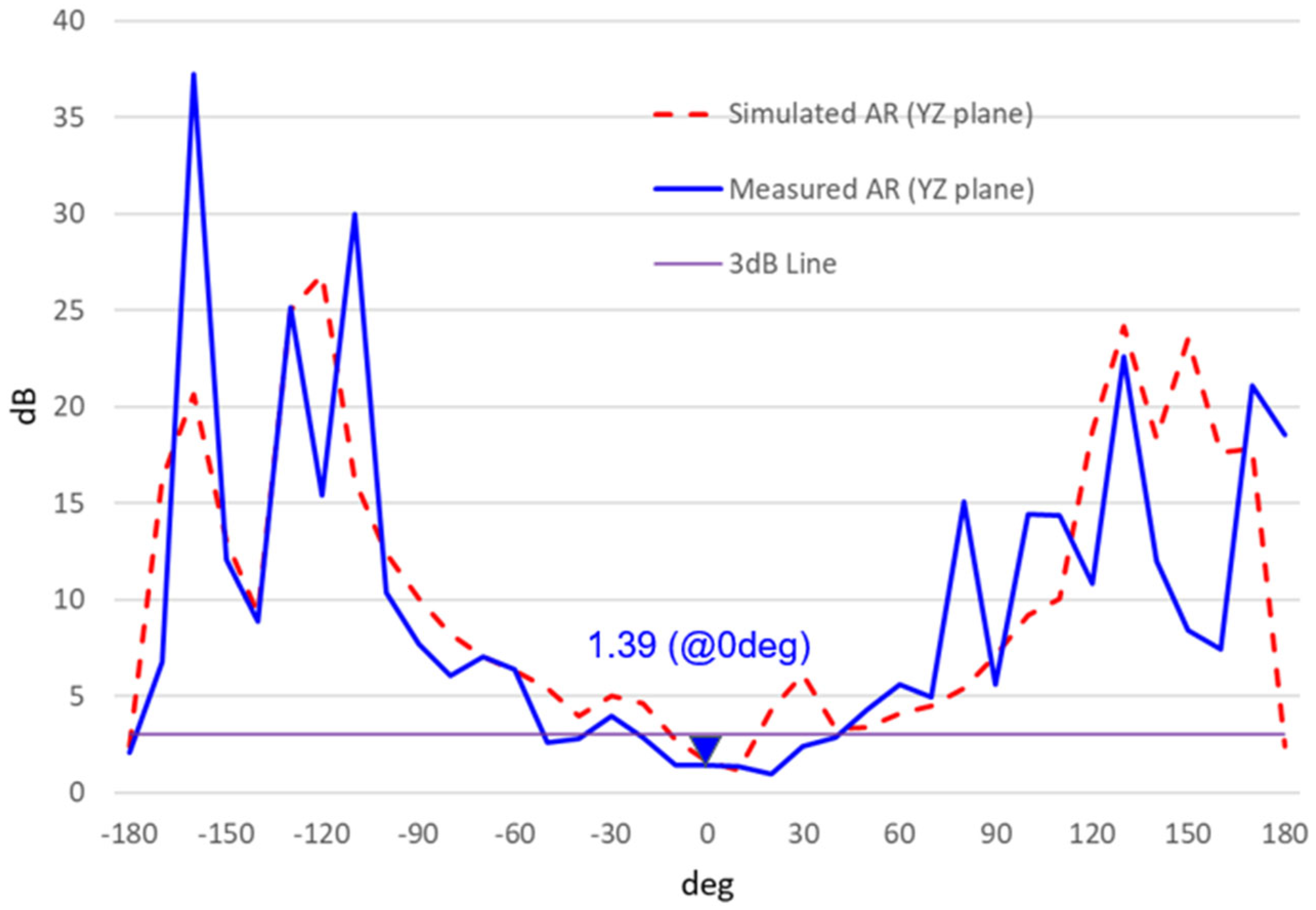
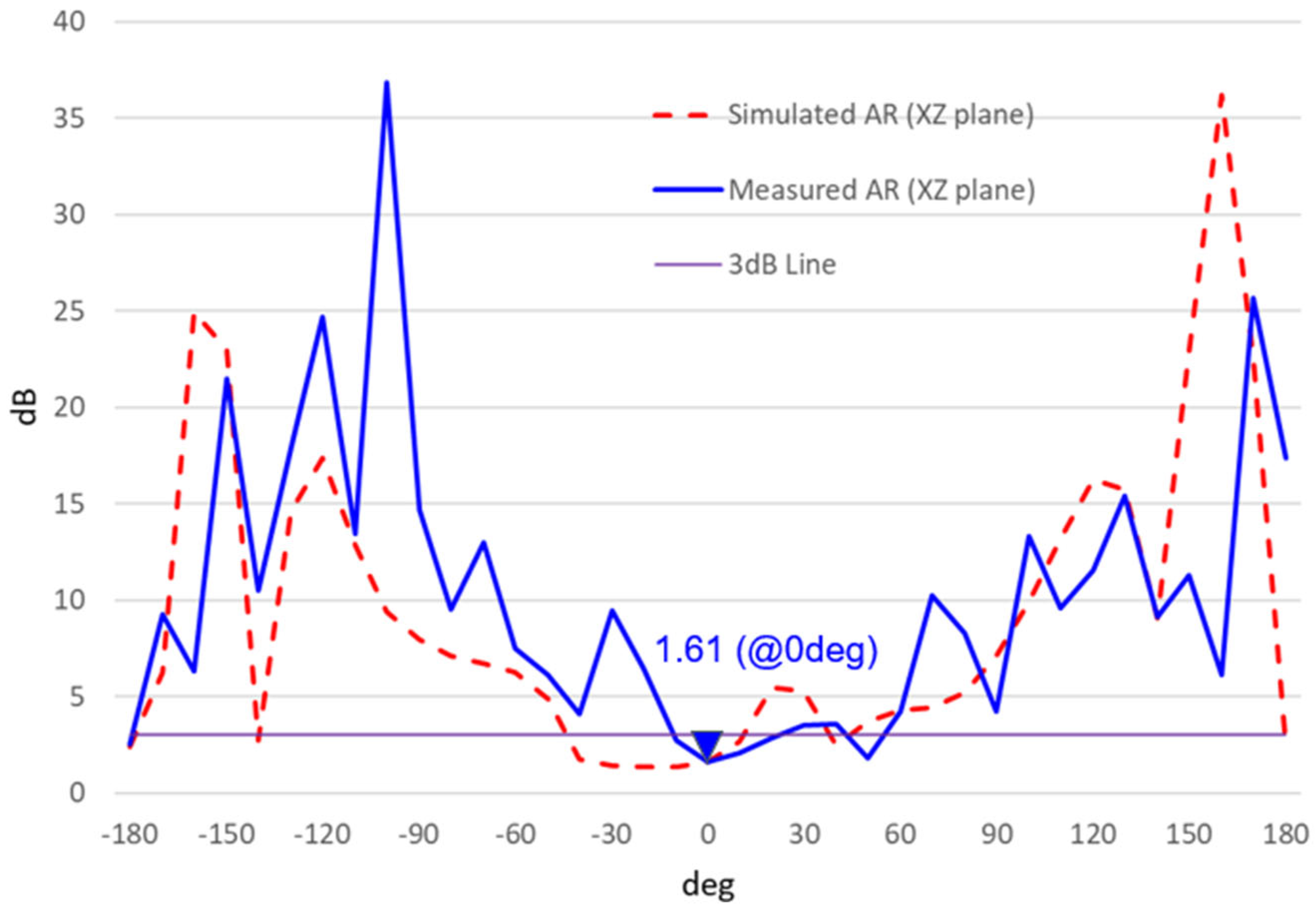
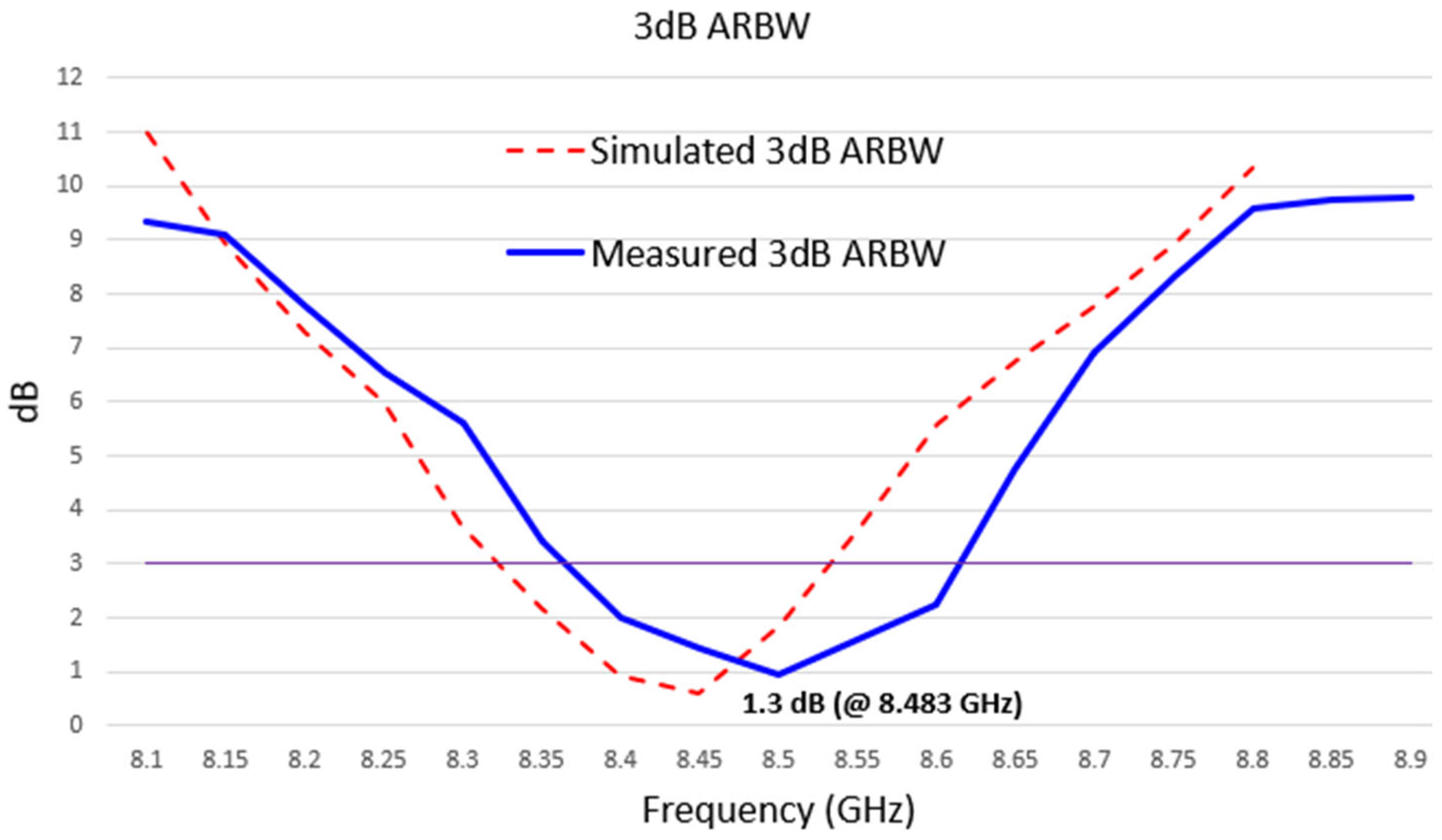
4. Antenna Measurement Results

The prototype of the CP EBG MPA was manufactured to validate the simulation results. The return loss S11 was measured using a Vector Network Analyzer (VNA). Figure 13 presents the fabricated MPA and our 3U CubeSat mockup model. As can be seen in Figure 13a, we had to use a total of 16 soldering nodes to fix the connecting vias to the EBG elements and the ground. In terms of structural robustness, this detail can be considered as a drawback of this fabricated antenna sample. However, we can improve this in the next fabricated samples by using plating technology to drill and firmly hold the vias between the top and the ground layers without the need for soldering.
In Figure 13b, the mockup model consists of the aluminum frame structure and mounting surfaces that closely replicate the mechanical interface of a 3U CubeSat. The dimensions of the model are 30 cm × 10 cm × 10 cm, and this structure can be considered as three 1U cubes stacked on top of each other. The CP EBG MPA prototype was mounted on one of the end surfaces of the mockup and tested in an anechoic chamber to evaluate its radiation characteristics under realistic boundary conditions. This test can provide an accurate evaluation of the antenna gain, polarization, and far-field radiation pattern while accounting for the potential influence of the satellite structure. The anechoic chamber test setup is illustrated in Figure 14, in which we use a pair of two X-band, left-hand and right-hand circular polarization (LHCP and RHCP) helical antennas to receive the electromagnetic wave radiated from our antenna under test (AUT). The received signals are processed by our software to plot the far-field radiation patterns and to evaluate the quality of the CP wave.
The process of qualifying the circular polarization of an antenna using two helical antennas is as follows: Firstly, we use the RHCP helical antenna to receive the radiated electromagnetic wave of our AUT (which is also RHCP) at 8.483 GHz, and record the spatial received power values (in dB) over the azimuthal plane. Then, we repeat this step but replace the RHCP helical antenna with the LHCP one to record the spatial received power values in this case. Secondly, we determine the cross polarization discrimination (XPD) values (in dB) using the following formula:
XPD = Received Power (RHCP) − Received Power (LHCP)
After that, we calculate the spatial axial ratio (AR) values over the azimuthal plane at the target frequency of 8.483 GHz using the following formula:
A R = l o g 10 X P D / 20 + 1 10 X P D / 20 1
To determine the 3 dB axial ratio bandwidth (3 dB ARBW), we repeated the above steps in a frequency span that surrounds our target frequency.
Figure 15 displays the measured S11 values of the CP EBG MPA. As observable in this figure, the measured return loss values at 8.483 GHz are approximately −15.4 dB, which is slightly higher than the simulated results. The reasons for this decrease are probably due to the discrepancies in the antenna manufacturing process. However, the measured −10 dB operational bandwidth is around 900 MHz, which is wider than the simulated result. The measured far-field radiation patterns in the YZ and XZ planes are shown in Figure 16. It is evident in these figures that the shapes of the measured patterns have good agreement with the simulation results. Furthermore, the measured gain is about 11.5 dBi along the radiation direction at 8.483 GHz, which is only 0.2 dB lower than the simulation.
The measured spatial axial ratios at 8.483 GHz in the YZ and XZ planes are presented in Figure 17 and Figure 18. As can be seen in these figures, the AR remains below the 3 dB threshold over an angular regions of 60° in the YZ plane and 30° in the XZ plane around the boresight, and the YZ plane value is slightly better than the XZ plane value, for example, 1.4 dB in compared with 1.6 dB at 8.483 GHz. This performance can be attributed to the high rotational symmetry of the EBG-based structure, which ensures polarization stability across orthogonal planes and mitigates the depolarization effects. The results highlighted the effectiveness of our proposed design in maintaining the CP quality, especially in dynamic orientation scenarios of the satellite platform when operating in orbit. The measured 3 dB ARBW over frequencies is shown in Figure 19. In this figure, the measured 3 dB ARBW is around 250 MHz (from 8.37 GHz to 8.62 GHz), which is better than the simulated result. These measured results confirmed the CP characteristics of the antenna.
A summary of the CP EBG antennas is tabulated in Table 3, and a comparison of our work and other X-band and near-X-band microstrip patch antennas, including other authors’ research and commercial antennas, is listed in Table 4.

5. Conclusions

A high-gain, circularly polarized X-band microstrip patch antenna designed for CubeSat applications is presented in this paper. The gain enhancement is achieved by applying a 16-element ring of electromagnetic band-gap structures surrounding the center radiator. The right-hand circular polarization is formed by etching two square slots symmetrically along the right diagonal line of the center radiator. The antenna is simulated and tested together with 3U CubeSat Platforms to evaluate the potential interference of the satellite platform with the antenna performance. The measured input reflection coefficient, far-field antenna pattern, axial ratio and 3 dB axial ratio bandwidth agreed well with the simulation results. The antenna gain is around 11.72 dBi and the spatial axial ratio is about 1.4 dB at the target frequency of 8.483 GHz, and the 3 dB ARBW is approximately 250 MHz. All these measured results satisfied our minimum antenna design requirements. With this EBG MPA design, we can boost the antenna gain more than two times (3.5 dB) without improving the total height of the antenna structure, and use only one layer of an EBG, thus maintaining the advantage of the low profile of the microstrip patch antenna. Furthermore, the measurements showed that the effect of the satellite structure model to the antenna radiation efficiency is negligible. The low profile and simple design of this antenna make it suitable for current CubeSat platforms. Our future work will focus on increasing the gain more by further studying different EBG and metamaterial topologies, while keeping the simplicity and robustness of the antenna structure.

Author Contributions

Conceptualization, L.P.T. and D.N.; methodology, L.P.T.; software, L.P.T. and M.H.; validation, L.P.T. and D.N.; data curation, L.P.T.; writing—original draft presentation, L.P.T.; writing—reviewing and editing, D.N. and M.H.; visualization, L.P.T.; supervision, D.N.; project administration, D.N.; funding acquisition, D.N. All authors have read and agreed to the published version of the manuscript.

Funding

This work was supported in part by the Foundation for Advancement of Industry Science and Technology (FAIS) Research and Development Grant and JSPS KAKENHI Grant Number 24K17455.

Data Availability Statement

The original contributions presented in this study are included in the article. Further inquiries can be directed to the corresponding author.

Conflicts of Interest

The authors declare no conflict of interest.

References

  1. Ghaderi, M.R.; Amiri, N. CubeSat Antenna Designs in the Last 2 Decades (2002–2023): A Survey. Int. J. Aeronaut. Space Sci. 2024, 26, 327–375. [Google Scholar] [CrossRef]
  2. Chahat, N.; Decrossas, E.; Kobayashi, M.M. Mars Cube One. In CubeSat Antenna Design, 1st ed.; Nacer, C., Ed.; Wiley-IEEE Press: Hoboken, NJ, USA, 2021; pp. 35–89. [Google Scholar] [CrossRef]
  3. Simone, M.; Lodi, M.B.; Curreli, N.; Pavone, S.C.; Maccio, C.; Marongiu, E.; Mariani, L.; Muntoni, G.; Mazzarella, G.; Fanti, A. A Deep Space Ka-band Antenna for CubeSat: Design and Multiphysics Analysis. In Proceedings of the 2022 16th European Conference on Antennas and Propagation (EuCAP), Madrid, Spain, 27 March–1 April 2022; pp. 1–5. [Google Scholar] [CrossRef]
  4. Byrne, B.; Capet, N.; Romier, M. Compact S-band and X-band antennas for CubeSats. CEAS Space J. 2020, 12, 587–596. [Google Scholar] [CrossRef]
  5. High-Gain Circularly Polarised Planar Antennas for Cubesat Systems. Available online: https://www.electronicspecifier.com/products/communications/high-gain-circularly-polarised-planar-antennas-for-cubesat-systems (accessed on 13 March 2025).
  6. CubeSat Design Specification Rev. 14.1. The CubeSat Program, Cal Poly SLO. Available online: https://static1.squarespace.com/static/5418c831e4b0fa4ecac1bacd/t/62193b7fc9e72e0053f00910/1645820809779/CDS%2BREV14_1%2B2022-02-09.pdf? (accessed on 18 April 2025).
  7. Babuscia, A. Telecommunication Systems for Small Satellites Operating at High Frequencies: A Review. Information 2020, 11, 258. [Google Scholar] [CrossRef]
  8. Zoubiri, B.; Mayouf, A.; Mayouf, F.; Abdelkebir, S.; Devers, T. Rectangular microstrip antenna gain enhancement using elliptical EBG structure. In Proceedings of the 2016 7th International Conference on Sciences of Electromagnetics, Technologies of Information and Telecommunications (SETIT), Hammamet, Tunisia, 18–20 December 2016; pp. 386–388. [Google Scholar] [CrossRef]
  9. Singh, D.; Thakur, A.; Srivastava, V.M. Miniaturization and Gain Enhancement of Microstrip Patch Antenna Using Defected Ground with EBG. J. Commun. 2018, 13, 730–736. [Google Scholar] [CrossRef]
  10. Rao, N.; Dinesh, K.V. Gain enhancement of microstrip patch antenna for Wi-Fi applications. In Proceedings of the 2014 Loughborough Antennas and Propagation Conference (LAPC), Loughborough, UK, 10–11 November 2014; pp. 312–315. [Google Scholar] [CrossRef]
  11. Errifi, H.; Baghdad, A.; Badri, A.; Sahel, A. Improving Microstrip Patch Antenna Directivity using EBG Superstrate. Am. J. Eng. Res. 2014, 3, 125–130. [Google Scholar]
  12. Qu, D.; Shafai, L.; Foroozesh, A. Improving microstrip patch antenna performance using EBG substrates. IEE Proc.-Microw. Antennas Propag. 2007, 153, 558–563. [Google Scholar] [CrossRef]
  13. Nasimuddin, N.; Chen, Z.N.; Qing, X. Slotted Microstrip Antennas for Circular Polarization with Compact Size. IEEE Antennas Propag. Mag. 2013, 55, 124–137. [Google Scholar] [CrossRef]
  14. Yablonovitch, E. Photonic Crystals. J. Mod. Opt. 1994, 41, 173–194. [Google Scholar] [CrossRef]
  15. Rahmat-Samii, Y.; Mosallaei, H. Electromagnetic band-gap structures: Classification, characterization, and applications. In Proceedings of the 2001 Eleventh International Conference on Antennas and Propagation, Manchester, UK, 17–20 April 2001; pp. 560–564. [Google Scholar] [CrossRef]
  16. Yang, F.; Rahmat-Samii, Y. Electromagnetic Band Gap Structures in Antenna Engineering; Cambridge University Press: Cambridge, UK, 2008; pp. 2–4. [Google Scholar]
  17. Sievenpiper, D.; Zhang, L.; Broas, R.; Alexopolous, N.; Yablonovitch, E. High-impedance electromagnetic surfaces with a forbidden frequency band. IEEE Trans. Microw. Theory Tech. 1999, 47, 2059–2074. [Google Scholar] [CrossRef]
  18. Li, L.; Li, B.; Liu, H.-X.; Liang, C.-H. Locally resonant cavity cell model for electromagnetic band gap structures. IEEE Trans. Antennas Propag. 2006, 54, 90–100. [Google Scholar] [CrossRef]
  19. Bharamappa, K.; Jagadeesha, S. Gain Enhancement of Microstrip Antenna using Ebg Structure for Wi-Fi Application. Int. J. Eng. Adv. Technol. 2019, 9, 1213–1217. [Google Scholar] [CrossRef]
  20. Ketkuntod, P.; Hongnara, T.; Thaiwirot, W.; Akkaraekthalin, P. Gain enhancement of microstrip patch antenna using I-shaped Mushroom-like EBG structure for WLAN application. In Proceedings of the 2017 International Symposium on Antennas and Propagation (ISAP), Phuket, Thailand, 30 October–2 November 2017; pp. 1–2. [Google Scholar] [CrossRef]
  21. Sharma, G.K.; Sharma, N. Improving the Performance Parameters of Microstrip Patch Antenna by Using EBG Substrate. Int. J. Res. Eng. Technol. 2013, 2, 111–115. [Google Scholar] [CrossRef]
  22. Abdulhameed, M.; Isa, M.S.B.M.; Zakaria, Z.; Ibrahim, I.M.; Mohsen, M.K.; Attiah, M.L.; Dinar, A.M. Radiation control of microstrip patch antenna by using electromagnetic band gap. AEU-Int. J. Electron. Commun. 2019, 110, 152835. [Google Scholar] [CrossRef]
  23. Abdulhameed, M.K.; Isa, M.S.M.; Zakaria, Z.; Mohsin, M.K.; Attiah, M.L. Mushroom-Like EBG to Improve Patch Antenna Performance for C-Band Satellite Application. Int. J. Electr. Comput. Eng. 2019, 8, 3875–3881. [Google Scholar] [CrossRef]
  24. Yang, F.; Rahmat-Samii, Y. Microstrip antennas integrated with electromagnetic band-gap (EBG) structures: A low mutual coupling design for array applications. IEEE Trans. Antennas Propag. 2003, 51, 2936–2946. [Google Scholar] [CrossRef]
  25. Tan, M.M.; Rahman, T.A.; Rahim, S.K.A.; Ali, M.T.; Jamlos, M.F. Antenna array enhancement using mushroom-like electromagnetic band gap (EBG). In Proceedings of the Fourth European Conference on Antennas and Propagation, Barcelona, Spain, 12–16 April 2010. [Google Scholar]
  26. Sokunbi, O.; Attia, H.; Sheikh, S.I. Microstrip Antenna Array with Reduced Mutual Coupling Using Slotted-Ring EBG Structure for 5G Applications. In Proceedings of the 2019 IEEE International Symposium on Antennas and Propagation and USNC-URSI Radio Science Meeting, Atlanta, GA, USA, 7–12 July 2019; pp. 1185–1186. [Google Scholar] [CrossRef]
  27. Jaglan, N.; Gupta, S.D. Surface waves minimisation in microstrip patch antenna using EBG substrate. In Proceedings of the 2015 International Conference on Signal Processing and Communication (ICSC), Noida, India, 16–18 March 2015; pp. 116–121. [Google Scholar] [CrossRef]
  28. Coccioli, R.; Yang, F.-R.; Ma, K.-P.; Itoh, T. Aperture-coupled patch antenna on UC-PBG substrate. IEEE Trans. Microw. Theory Tech. 1999, 47, 2123–2130. [Google Scholar] [CrossRef]
  29. Gonzalo, R.; De Maagt, P.; Sorolla, M. Enhanced patch-antenna performance by suppressing surface waves using photonic-bandgap substrates. IEEE Trans. Microw. Theory Tech. 1999, 47, 2131–2138. [Google Scholar] [CrossRef]
  30. Colburn, J.; Rahmat-Samii, Y. Patch antennas on externally perforated high dielectric constant substrates. IEEE Trans. Antennas Propag. 1999, 47, 1785–1794. [Google Scholar] [CrossRef]
  31. CubeSat Concept. Available online: https://www.eoportal.org/other-space-activities/cubesat-concept#p-pod-poly-picosatellite-orbital-deployerta (accessed on 17 March 2025).
  32. Toorian, A.; Diaz, K.; Lee, S. The CubeSat Approach to Space Access. In Proceedings of the 2008 IEEE Aerospace Conference, Big Sky, MT, USA, 1–8 March 2008; pp. 1–14. [Google Scholar] [CrossRef]
Figure 1. (a) A demonstration of two adjacent elements of the mushroom-like EBG, a top view and side view; (b) an illustration of the capacitive and inductive components, and the equivalent parallel LC circuit of this EBG structure. The red arrow indicates the inductive path between the ground and the EBG patches.
Electronics 14 02216 g001
Figure 2. Examples of the deployment of a mushroom-like EBG structure: (a) the single-element MPA and (b) the MPA array.
Electronics 14 02216 g002
Figure 3. (a) The 1U CubeSat primary structure; (b) the available zone for antenna mounting.
Electronics 14 02216 g003
Figure 4. The design of X-band EBG MPAs for circular polarization: (a) overview and (b) zoom-in of the center patch radiator. The grey circle is the contacting part of the SMA probe feed.
Electronics 14 02216 g004
Figure 5. The simulated S11 values of the original and the CP EBG MPAs.
Electronics 14 02216 g005
Figure 6. The simulated gains over frequencies of the original and the CP EBG MPAs.
Electronics 14 02216 g006
Figure 7. The simulated far-field radiation patterns of (a) the original MPA and (b) the CP EBG MPA. The red lines are the main pattern curves and the blue lines mark the 3dB angular widths.
Electronics 14 02216 g007
Figure 8. The surface current distribution at ωt = 90° of (a) the original MPA and (b) the CP EBG MPA.
Electronics 14 02216 g008
Figure 9. The simulated 3 dB axial ratio bandwidth of the CP EBG MPA.
Electronics 14 02216 g009
Figure 10. The experimental EBG MPAs from Case (a), with the initial EBG, to Case (h), with the final EBG design.
Electronics 14 02216 g010
Figure 11. The gains over frequencies of the experimental EBG MPAs from Case (a) to Case (h).
Electronics 14 02216 g011
Figure 12. The gains over frequencies of the EBG MPA when varying the dimensions of the EBG elements.
Electronics 14 02216 g012
Figure 13. (a) The fabricated CP EBG MPA; (b) the structure of the 3U CubeSat model; (c) the antenna after being integrated into the CubeSat model.
Electronics 14 02216 g013
Figure 14. The anechoic chamber setup for the antenna radiation pattern measurement.
Electronics 14 02216 g014
Figure 15. The measured S11 of the CP EBG MPA.
Electronics 14 02216 g015
Figure 16. The measured radiation patterns of the CP EBG MPA in (a) the YZ plane and in the (b) XZ plane.
Electronics 14 02216 g016
Figure 17. The measured spatial AR at 8.483 GHz in the YZ plane.
Electronics 14 02216 g017
Figure 18. The measured spatial AR at 8.483 GHz in the XZ plane.
Electronics 14 02216 g018
Figure 19. The measured 3 dB ARBW over frequencies.
Electronics 14 02216 g019
Table 1. The minimum antenna design requirements.
NameValue
Gain10 dBi
Gain Bandwidth13 MHz
S11 Bandwidth13 MHz
AR Bandwidth13 MHz
Table 2. The antenna parameters.
NameValueDescription
Lp10Patch length
Wp10Patch width
Lg91.3Ground length
Wg91.3Ground width
Lebg10Length of an EBG element
Webg10Width of an EBG element
gebg2Gap between two adjacent EBGs
lsl14Length of the upper square
wsl14Width of the upper square
lsl23Length of the lower square
wsl23Width of the lower square
le10.5Distance from the upper square to the upper edge
we10.5Distance from the upper square to the right edge
le21Distance from the lower square to the lower edge
we21Distance from the lower square to the left edge
lcor15Truncated corner length
wcor15Truncated corner width
h1.6Substrate thickness
hc0.035Conductive part thickness
Table 3. The summary of our proposed EBG antennas.
Antenna ParametersSpecificationsUnits
Operation frequency8.483GHz
−10 dB Impedance bandwidth900MHz
PolarizationRHCP-
Measured Gains11.72dBi
Measured AR at 8.483 GHz1.4dB
Measured 3 dB ARBW250MHz
Antenna efficiency95%
Dielectric substrateRogers RT5880-
RF input50
Feed typeSingle probe (SMA)
Table 4. Comparison of our work with other X-band and near-X-band MPAs.
Ref. No.Center Freq. (GHz)Antenna Size
(mm)
Max. Gain (dBi)PolarizationRemarks
[4]8.272.6 × 72.6 × 1111.5CP- Complicated design.
- Feed network needed.
- The height exceeded the 6.5 mm threshold specified in Cal Poly’s CDS.
[5]8.25100 × 10017 (dBic)CP- Need 4 feed points to create differential pairs of excited signals for CP.
- The height is not mentioned. However, it exceeded 6.5 mm and cannot be applied to CubeSats that follow Cal Poly’s CDS.
[7]7.19 (RX)
8.45 (TX)
120 × 809CP- Too big for 1U CubeSat surface.
- Feed network needed.
- The height is not mentioned.
[11]760 × 4511.78
(directivity)
LP- Only simulation result of the directivity, not the realized gain.
- The height is not mentioned. However, the 2 EBG superstrates makes the structure too high to apply to CubeSats that follow Cal Poly’s CDS.
[12]9.960 × 60 × 3.29.77LP- Complicated design with mushroom-like EBG as the middle layer.
- The airgap between layers can significantly affect the antenna performance.
[21]10.6750 × 357.7LP- The gain is not so high.
- No measured results. Only simulation.
- The height is not mentioned.
Our work8.4891.3 × 91.3 × 1.611.72CP- Simple design.
- No feed network needed.
- Highly compatible with CubeSat platforms.
Disclaimer/Publisher’s Note: The statements, opinions and data contained in all publications are solely those of the individual author(s) and contributor(s) and not of MDPI and/or the editor(s). MDPI and/or the editor(s) disclaim responsibility for any injury to people or property resulting from any ideas, methods, instructions or products referred to in the content.

