1. Introduction
Modern power converters have transformed the motor drive industry with the introduction of adjustable-speed drive (ASD) technology. ASDs enhance a system’s energy efficiency by controlling the motor’s speed and/or torque to operate at optimal levels. As a result, the motor’s energy consumption is decreased from full power to partial power while maintaining the same performance [
1]. It has been seen that more than 40% of electrical energy is consumed by motor driven systems, which makes motor drives the major consumer of electricity globally [
2]. This leads industries to adopt ASD systems to reduce consumption of electricity and improve motor efficiency [
3].
Normally, high-power motor drives operate in three-phase systems and use double-stage converters. The first stage, known as the front end, is equipped with an AC/DC rectifier to convert the AC power to DC, while the second stage, commonly known as rear-end, is equipped with an inverter to convert the DC power back to AC with the desired voltage and frequency to control the motor’s speed and/or torque [
4]. Usually, a DC-link capacitor is utilized in the DC side to flatten the DC voltage and circulate rear-end harmonics. Since the front-end converter interacts directly with the distribution grid, it is considered as one of the main contributors of the harmonics injected to the grid [
5]. Therefore, front-end rectifiers gain a lot of research interest.
Active front-end systems that rely on voltage source inverters (VSI) present prominent topologies that can shape the input current to an almost pure sine wave with minimum current harmonics injection to the grid. In addition, they have the ability to perform bidirectional power follow [
6,
7,
8,
9]. However, since ASDs rarely use bidirectional power follow, the control complexity and high cost of using active switches make VSIs uncommon topologies for use as front-end rectifiers. Additionally, 12-pulse and 18-pulse rectifiers can be utilized as frond-end rectifiers, which could reduce the current harmonics injection to the grid due to the increase in pulses [
10,
11]. However, 12-pulse and 18-pulse rectifiers could limit the power factor. In addition, the transformer is bulky, which increases the size and cost of ASD systems.
International standards such as IEEE-519 [
12] and IEC61000-3-12 [
13] allow moderately high levels of harmonics to be injected to the grid. In table-4 of IEC61000-3-12, the permissible current harmonics injection from ASD reaches a THDi of 48%, with 40% being the fifth harmonic. Subsequently, three-phase diode rectifiers (DRs) with passive filters are common topologies that have been utilized as a front end in a wide range of ASDs in different industries [
14]. Although three-phase diode rectifiers are reliable and cost effective, their high emission of current harmonics under partial power, which ASD most of the time tends to operate at, makes them unattractive [
15].
An electronic inductor (EI) topology shown in [
16,
17,
18] presents a simple method based on a boost converter that can be utilized as an intermediate circuit. The boost converter can emulate an infinite inductor to shape the input current as a square wave. In this case, the ASD will maintain a fixed THDi of 30% under full and partial power. Furthermore, a control technique based on a modulated pulse pattern can be used with EI for further specific harmonics mitigation [
19,
20]. However, harmonics emissions of the ASD are considered relatively high even after utilizing the EI. In [
21,
22], multi-parallel rectifiers with a common DC-link are presented to show additional harmonics reduction. However, in order to achieve a reduction of less than 7% THDi, five parallel diode and silicon-controlled rectifiers need to be installed. This could lead to an increase in the cost and size of the ASD system.
In single phase systems, power factor correction (PFC) circuits are widely used at different power levels as a replacement of conventional single phase DRs with passive filters due to their low cost and their ability to shape the input current as a sine wave [
23]. While in three-phase systems, three-phase PFCs have not been considered as replacements for three-phase DR front ends for ASD systems in the literature.
In this paper, a three-phase PFC with a common DC-link is proposed as a front-end stage for ASD systems. The proposed topology is based on utilizing three single-phase PFCs, and each of them is connected to a different line-line voltage with a common DC-link. Then, the DC-link bus can be shared for multi motor drives. A shared current controller is used to ensure balanced input currents while maintaining the DC-link voltage at the desired level. The following parts of this paper are organized as follows.
Section 2 provides a detailed background about conventional three-phase DR with different filtering topologies. Then, the structure of the proposed method and control strategy is discussed in
Section 3.
Section 4 presents the simulation results of the proposed system under different power levels. Finally, a conclusion and summary are presented in
Section 5.
3. Proposed Three-Phase PFC with Common DC-Link
As discussed in the previous section, the conventional three-phase DR has several drawbacks, including high current harmonic injection into the grid, which can potentially increase under partial power conditions, as seen in
Figure 1. These harmonics lead to increased system losses and impair the network. Thus, the proposed three-phase PFC is a cost-effective solution that can be used as a front end for ASD systems. The proposed topology not only significantly improves current harmonics and shapes the input currents into sine waves but also allows sharing of the DC-link voltage across multiple motor drives. The unique benefit of the proposed topology lies in its design and control approach, enabling the system to operate effectively with a shared DC-link voltage.
3.1. Method
The architecture of the proposed three-phase PFC system is illustrated in
Figure 4. In this system, three single-phase DRs are connected to three different line-to-line grid voltages. Then, three modified boost converters are utilized as an intermediate circuit, sharing the same output DC voltage, allowing multiple motor drives to share the DC-link voltage. These boost converters operate independently with current-sharing control to maintain the desired DC-link voltage and ensure sinusoidal input currents. To illustrate the operation of the system, the switching intervals of the first boost converter will be discussed, while the other two converters follow the same pattern.
The boost converter shown at the top of
Figure 4a operates as a conventional single-phase PFC connected to a line-to-line voltage, operating in continuous conduction mode (CCM). The duty cycle can be determined using the standard PFC equation, as shown in (1).
Since all three boost converters share the same output DC-link voltage, and to prevent circulating current between the converters when the switch (S1) is closed (ON), a freewheeling diode is inserted on the negative side of each boost converter (D2, D4, D6). The maximum voltage that S1, S2, and S3 see is the output voltage since the topology is a boost PFC. As long as the switch is chosen with a voltage blocking capability bigger than the output voltage, it will be suitable.
In this configuration, D2 becomes forward-biased when the switch is closed, forcing the current to return through DR-1. To illustrate,
Figure 4b depicts the circulating current between DR-1 and DR-2 in the absence of negative-side diodes. At specific moments, such as when u
a > u
b > u
c (e.g., at ωt = 120°) and when S1 is closed, the current from the DR-1 flows back through the DR-2, negatively impacting the phase-current waveforms. This issue can be effectively resolved by inserting the negative-side diodes.
Furthermore, to mitigate circulating current between the DRs when the switch is open (OFF), the boost inductor is split between the positive and negative sides. In this case, the negative-side inductor (L1
dc-) prevents a sudden change in current as described in (2). Although the voltage across the negative inductor differs from that of the positive inductor due to the circuit configuration, the circulating current between the DRs is limited, as will be demonstrated in the results section. Additionally, when the switch turns on again, D2 ensures that the current continues to return through DR-1.
The current controller of the boost converter shapes the inductor current to follow the rectified voltage . In this case, the input current iDR-1 will be a sine wave with a thirty-degree phase shift, following the line voltage uab. Consequently, the line current (ia) is the result of subtracting iDR-3 from iDR-1 producing a sine wave with zero phase angle, thereby ensuring unity power factor.
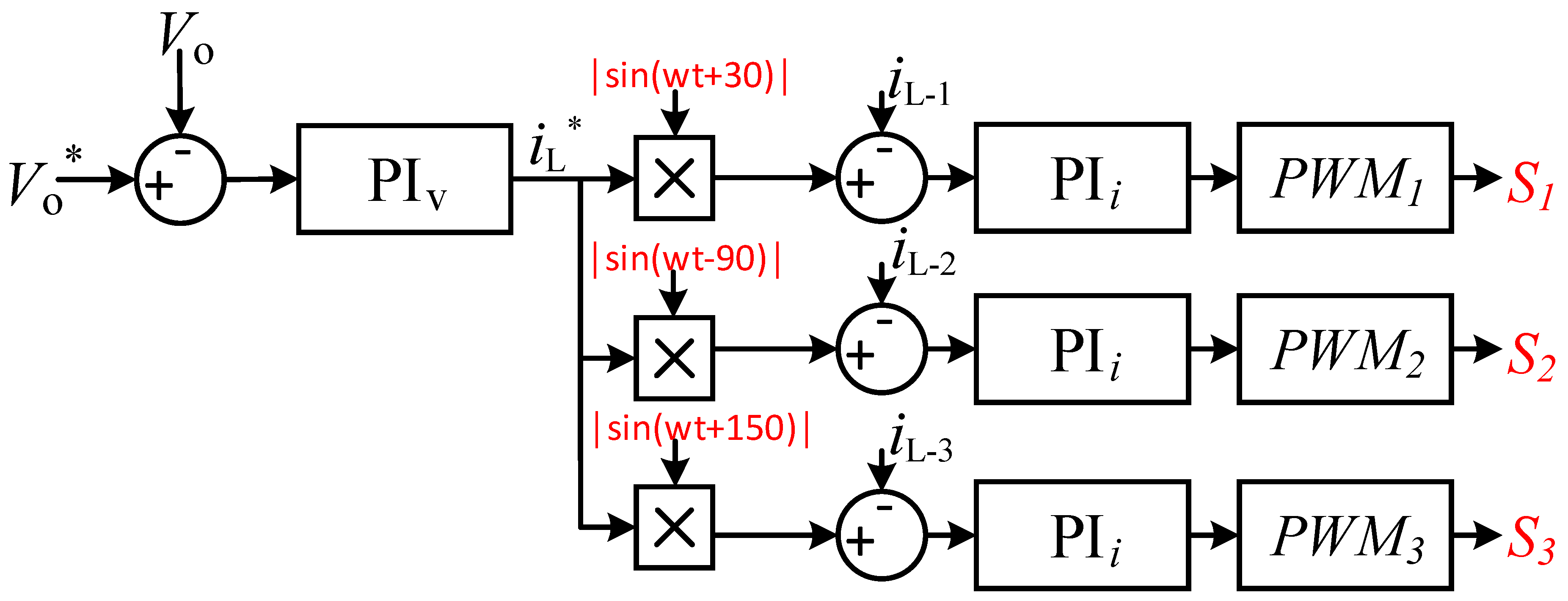
3.2. Control
Controlling the proposed three-phase PFC system is based on a two-loop control method, as illustrated in
Figure 5. The outer voltage loop regulates the DC-link voltage by measuring Vo and comparing it with the reference voltage. The resulting error signal (the difference between the reference voltage and the measured voltage) is processed by the outer loop’s proportional-integral controller (PI
V), which generates the reference inductor current. To ensure balanced operation of all three boost converters and consequently balanced three-phase input currents, a current-sharing control strategy is employed. The reference inductor current is equally distributed among the three inner current control loops, resulting in three balanced reference currents for the boost converters. Each reference current is then multiplied by its corresponding desired sine wave. The product is compared with the measured inductor currents (
iL-1,
iL-2,
iL-3) to generate error signals, which are fed to the inner current PI controllers (
PIi). The outputs of the
PIi controllers are sent to the PWM circuits to generate the switching duty cycles. As a result, all three inductor currents follow their respective rectified voltage waveforms, while containing high-order harmonics due to the switching action.
In this PI control scheme, a dual-loop control structure is employed: an external slow voltage-regulating loop and an internal fast current-regulating loop. The outer voltage loop regulates the output DC-link voltage by providing a current reference value, while the faster inner current loop regulates the inductor current to closely track this reference. Each PI controller is designed based on specific crossover frequency and phase margin criteria to achieve regulation within an acceptable time response. The inner current loop is designed with a high bandwidth of 4 kHz and a phase margin of 60°, ensuring a fast and stable current response. The outer voltage loop, on the other hand, is designed with a significantly lower bandwidth of 20 Hz and a phase margin of 50° to avoid interfering with the 120 Hz harmonics necessary in PFC applications. This design ensures that the voltage error is not corrected by the inner current control loop, as shown in (3). Conversely, the inner current control loop is designed using the high-frequency transfer function of the power stage, which relates the inductor current to the duty cycle, as shown in (4).
where
is the peak line-line input voltage, and
can be calculated as the square of the output voltage divided by the output power. The transfer functions shown in Equations (3) and (4) are then used to tune the inner and outer loop PI controllers using MATLAB’s Control System Designer. It should be noted that all inner current control loops (
PIi-1,
PIi-2,
PIi-3) use identical parameters to ensure equal current distribution among all three boost converters. By setting up this design criteria, the PI controllers design process becomes straight forward. The current to duty cycle transfer function is defined as follows:
The voltage-to-current transfer function is defined as follows:
Since the total phase of the open loop system must be –120 degrees to achieve a 60-degree margin, and the plant adds –90, the current controller must add –30 degrees. Since the PI controller’s transfer function is as follows:
Additionally, the complex value of it at the crossover frequency is as follows:
Therefore, the phase of this complex value is as follows:
Since this is desired to be -30 degrees:
Finally, taking the tangent of both sides yields the following:
At the crossover frequency, the open loop transfer function gain must equal unity:
By replacing the plant magnitude and the PI magnitude (i.e.,
) and taking into account the ratio between
and
that is found in (9), their value can be determined. The same procedure can be applied to the voltage loop. A phase margin of 50 degrees is set, and that defines the required open loop phase to be as follows:
The plant phase at the crossover frequency is defined as follows:
where
the chosen crossover frequency for the voltage is the loop, and
is the plant pole. The voltage PI phase and
to
ratio can now be determined:
Similar to the current controller, the open loop transfer function gain must be unity at the chosen crossover frequency:
By replacing the plant magnitude and the PI magnitude () and taking into account the ratio between and that is found in (10), their value can be determined.
4. Results
To validate the proposed three-phase PFC system, the configuration shown in
Figure 4 is implemented using MATLAB Simulink (R2024b). A 4 kW motor drive is considered as the output load. The parameters applied to the system are listed in
Table 1. The PI parameters are calculated using the design criteria and procedure described in the previous section, and the values are listed in
Table 2.
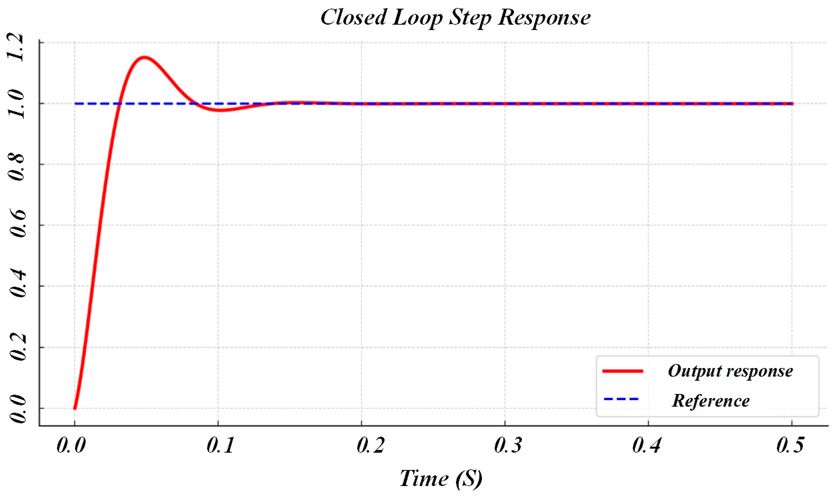
In the beginning, a step response test to the closed loop transfer function was performed to validate the stability and the responsiveness of the PI controller. Using the PI parameters that were calculated and shown in
Table 2, the step response test was as follows (
Figure 6).
The step test confirms that the dual-PI controller tracks its reference correctly, and the voltage rises to 1 in roughly 23 ms, which is consistent with the chosen crossover frequency of 20 Hz for the voltage loop. In addition, a step test was performed in the simulation, and a 50-volt step to the output reference was performed (
Figure 7):
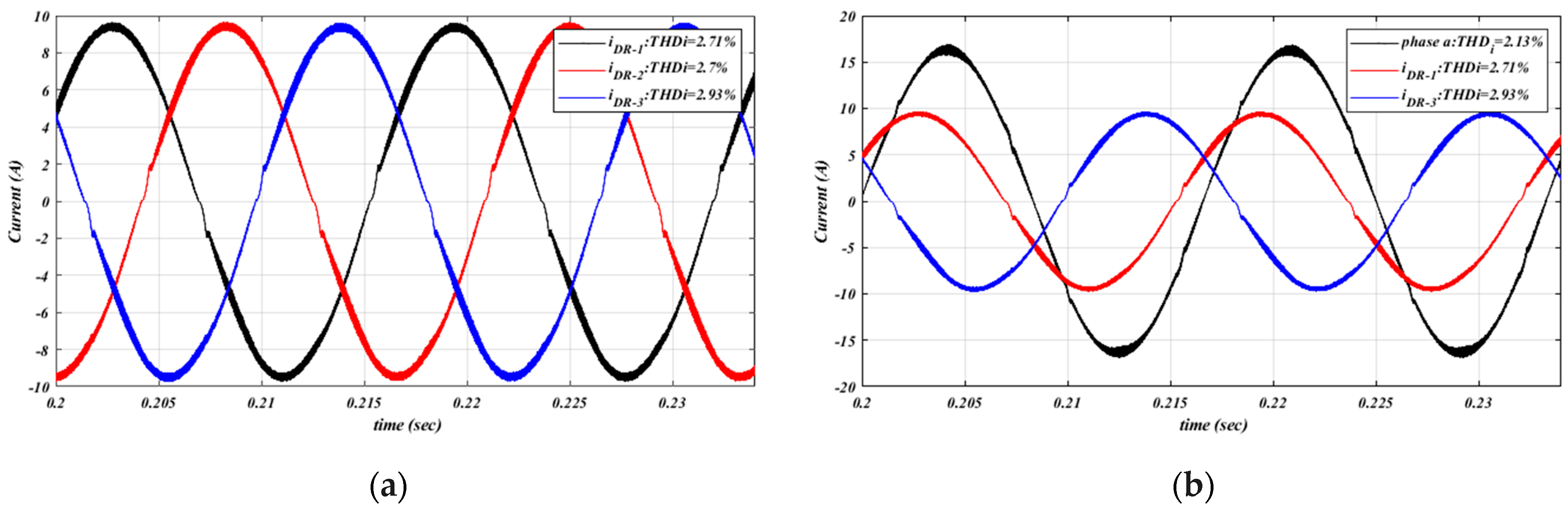
It can be seen that the output tracks the reference very well and with a modest overshoot, which validates the stability and response of the designed PI control structure. Since motor drives typically operate at partial load, and to evaluate the performance of the proposed method under various operating conditions, the system is tested at full rated power, 50%, and 25% of the rated power. The system is examined at the rated power of 4 kW, and
Figure 8a shows the input currents of all three diode rectifiers (
iDR-1,
iDR-2,
iDR-3). As can be seen from the
Figure 8a, the currents are shaped as sine waves, following the supplied line voltages to each rectifier, with a total harmonic distortion of current (THDi) around 2.7%. Consequently, the grid phase-a current is obtained by subtracting the input current of DR-3 from that of DR-1, as shown in
Figure 8b. The THDi of the phase-a current is slightly lower than that of the individual input currents, with a value of 2.13%. This reduction is attributed to harmonic cancellation between the input currents of DR-1 and DR-3.
Since the control method is based on balanced sharing among all three phases, the grid currents are expected to be balanced.
Figure 9a illustrates the grid currents of all three phases. As can be seen from the
Figure 9a, all grid currents are balanced sine waves with unity power factor. These currents exhibit low total harmonic distortion (THDi), approximately 2.15%. It should be noted that low order harmonics are very small, while most of the harmonics are concentrated around the switching frequency due to the PWM switching pattern, as shown for phase-a in
Figure 9b,c.
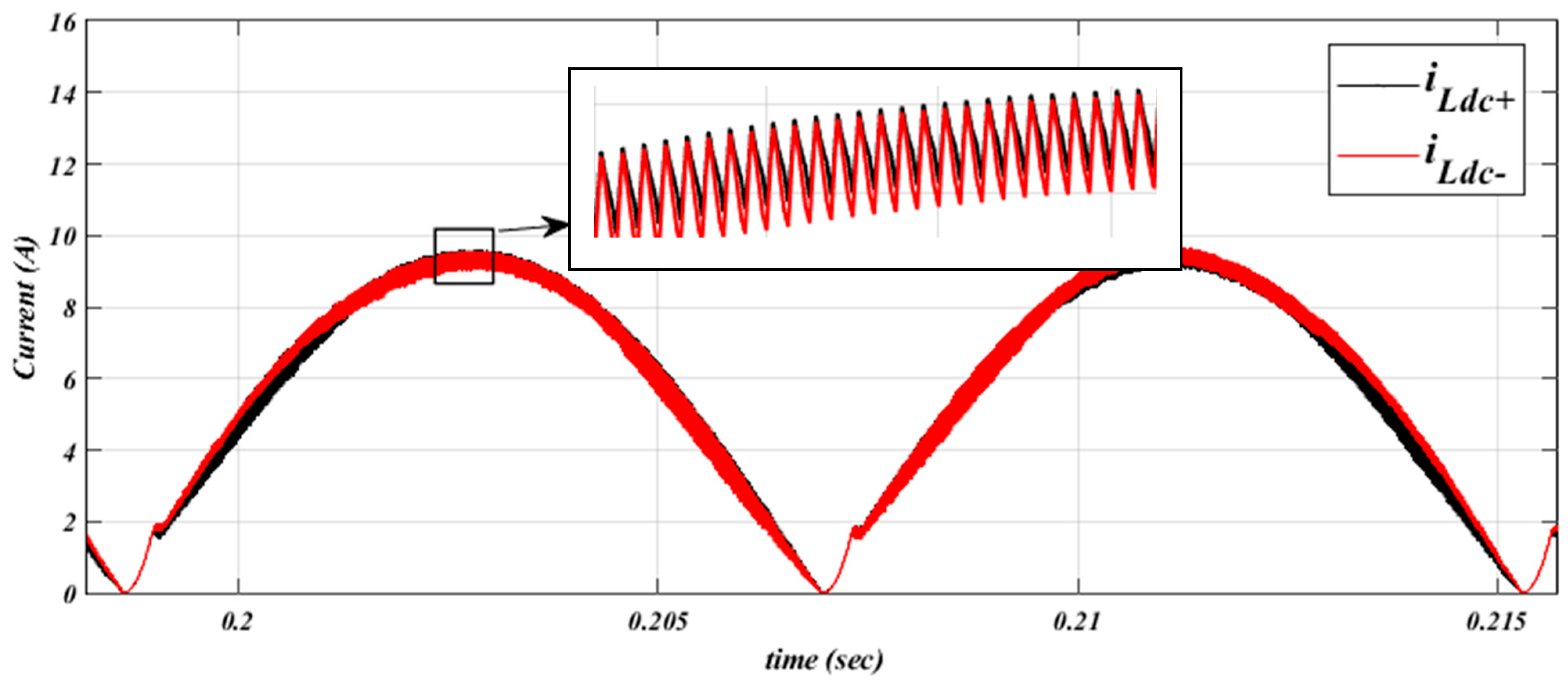
As discussed in the previous section, when the switch is ON, the negative-side diode forces the current to return through the negative-side inductor to the corresponding diode rectifier (DR). However, since the voltage across the positive-side inductor differs from that across the negative-side inductor during the ON state, a slight circulating current is induced between the DRs. This circulating current is mitigated by the presence of the negative-side inductor. Additionally, once the switch is ON, the negative-side diode continues to direct the return current through the negative-side inductor, as illustrated in
Figure 10.
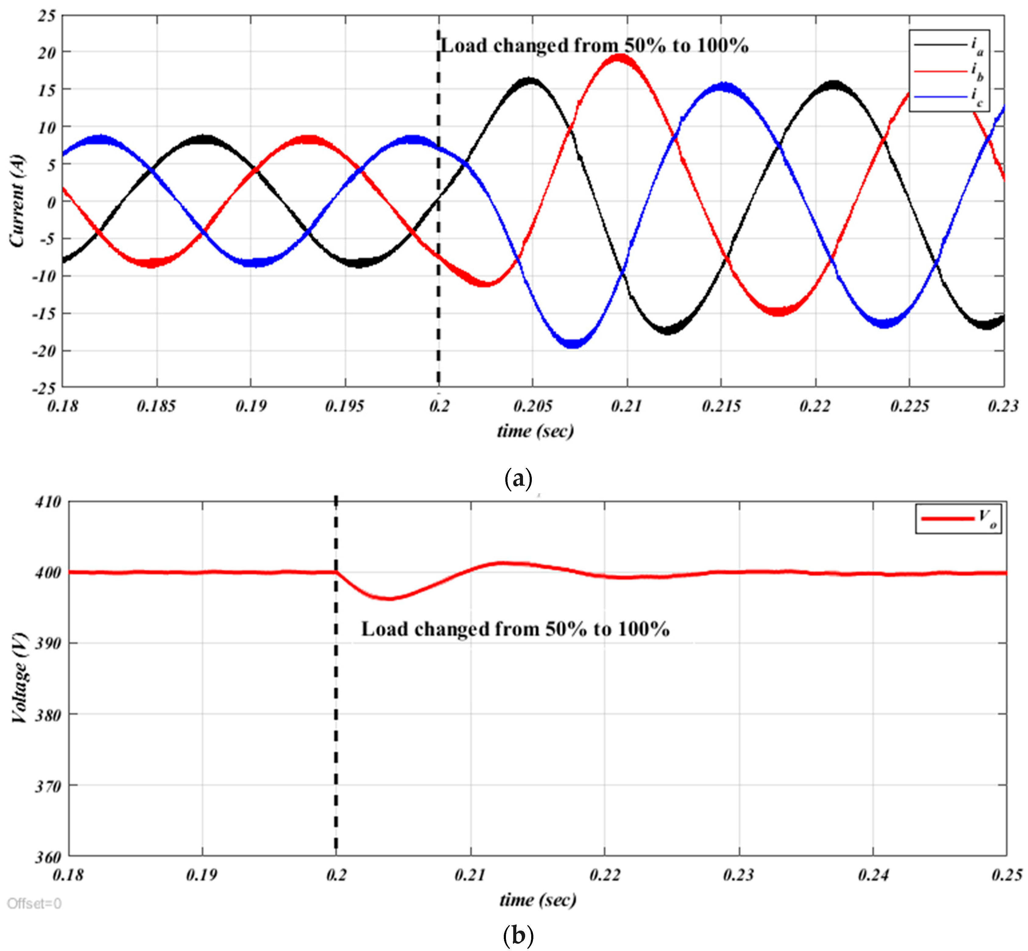
To demonstrate the effectiveness of the proposed control approach, the system’s behavior was evaluated under a sudden load increase from 50% to 100% at t = 0.2 s. While rapid load changes are not typically critical in motor-driven applications like pumps and compressors, a 50% step change was still examined for thoroughness.
Figure 11 illustrates the simulation results, depicting the grid currents and DC-link voltage. The currents transition smoothly to the new set point within approximately 0.016 s (one cycle). Meanwhile, the DC-link voltage experiences a minor temporary dip, decreasing from around 400 V to 396 V after the load change. This drop, amounting to about 1%, is quickly corrected by the DC-link control system, as analyzed in
Section 3.2, with recovery achieved in roughly 0.025 s. Overall, the proposed method demonstrates stability and reliability in handling abrupt load variations while maintaining consistent performance.
To evaluate the performance of the proposed system under partial load conditions, the system is tested at 50% and 25% of the rated power.
Figure 10 illustrates the grid currents at these operating points. As shown in
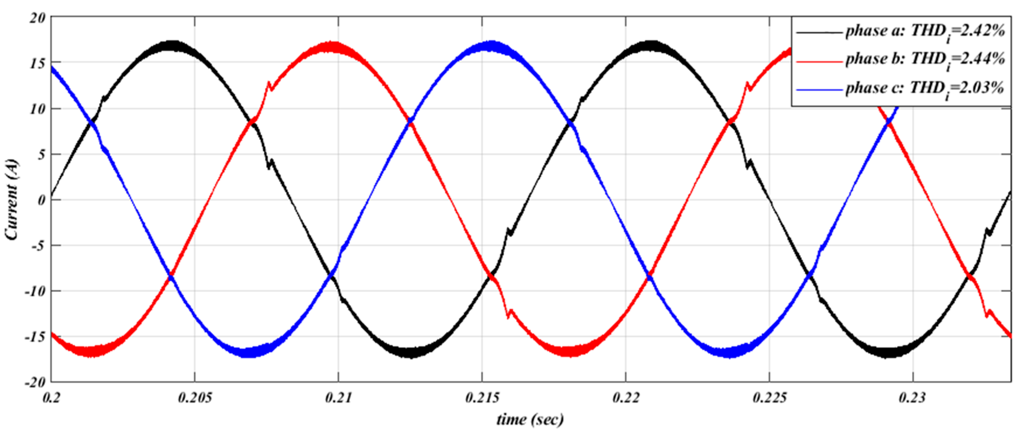
Figure 12a, when the system operates at half of the rated power, it maintains good performance, with grid current harmonics around 3.9%. When the system operates at 25% of the rated power, the grid current THDi increases to approximately 6.8%. These levels of harmonic distortion are acceptable, considering that the system parameters and controllers were designed based on the rated power rather than partial load conditions. Additionally, to simulate the system’s behavior with unbalanced input voltages, the voltage of phase-b was reduced to 90% of its normal level. Because each rectifier is linked to a line-to-line voltage, both DR-1 and DR-2 are affected by this change.
Figure 13 illustrates the grid current for all three phases, demonstrating that the system maintains balanced input currents at 11.95 A RMS. However, there is a minor increase in harmonic distortion in phase-a and phase-b, with THDi values of 2.42% and 2.44%, respectively, compared to phase-c’s THDi of 2.03%.
To evaluate the proposed system against the existing methods discussed in
Section 2, a comparison is provided in
Table 3, focusing on the number of elements, harmonic emissions, and efficiency. As shown in the table, the proposed system demonstrates significantly better THDi compared to the existing methods. While the passive filtering method exhibits higher efficiency than the proposed system, it suffers from the highest harmonic emission, with a THDi of 48%. The proposed system achieves efficiency levels comparable to EI and MMR but requires a greater number of diodes due to the incorporation of three single-phase diode rectifiers. It is important to note that the efficiency values are derived from simulations; however, in practical experiments, the influence of parasitic elements may slightly alter these results.
To sum up, the results demonstrate the good performance of the proposed three-phase PFC system across different power levels, validating both the system architecture and the shared current control method. The system successfully delivers sinusoidal input currents with unity power factor while maintaining the DC-link voltage at the designed reference level.


