1. Introduction
Capacitive proximity sensors (CPSs) stand out among various proximity sensors due to their attractive properties, including flexible and diverse structural design, low cost, low power consumption, and being non-intrusive and non-invasive. These advantages make CPSs ideal for a wide range of applications in industrial settings and smart environments [
1]. In modern industrial production lines, CPSs are widely preferred for the application of proximity switches. These switches are characterized by their ability to output a signal through contact closure or pulse transmission when the target reaches a specific distance threshold. In some specified contexts, such as wafer detection in solar cell manufacturing facilities, granule level detection in injection-molding plants, cylinder position detection, and the detection of automotive parts in place, capacitive proximity switches play a crucial roles [
2,
3].
While various proximity sensing technologies exist, capacitive methods offer distinct advantages for industrial applications requiring short-range detection. Compared with microwave-based approaches that utilize RF propagation (typically 1–100 GHz), capacitive sensors can achieve superior sensitivity to conductive targets at sub-50 mm ranges (0.1 mm resolution vs. microwave’s 0.01–0.05 mm). Meanwhile, CPSs can better tolerate metallic environments due to electric field confinement. However, microwave sensors maintain advantages in long-range detection (>1 m) and through-wall applications [
4,
5]. This work focused on the critical 0–45 mm industrial range where capacitive sensing provides optimal performance/cost tradeoffs.
Capacitive sensors can be classified into two groups: floating capacitive sensors, in which neither of the electrodes is grounded, and grounded capacitive sensors, in which one of the two electrodes is grounded [
6,
7,
8]. These two types of sensors are extensively applied in all kinds of fields. However, grounding one of the electrodes is necessary in some applications [
9,
10,
11,
12]. Grounded CPSs are susceptible to parasitic effects, stray capacitance, and distributed capacitance from the environment in practical environments, so shielding measures are often employed during their applications [
13]. Furthermore, capacitive proximity switches face two types of operating conditions: flush mounting (FM) and non-flush mounting (NFM), due to different installation surfaces.
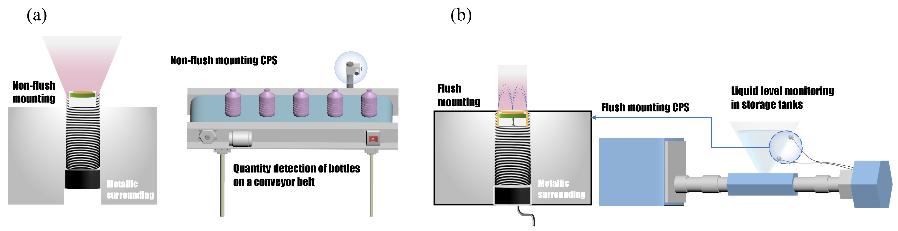
Flush mounting and non-flush mounting are two methods for installing CPSs in automated machines, robotics, and consumer products. In the NFM method, the sensor protrudes from the mounting surface, with its sensing face exposed and unshielded, as shown in
Figure 1a. This configuration allows the electric field to extend outward from both the front and sides of the sensor, leading to a larger sensing range. Meanwhile, in the FM approach, the sensor’s sensing face aligns perfectly with the surrounding surface, as shown in
Figure 1b. A metal shield encases the sensor, restricting the electric field’s distribution to solely the front face, which allows for seamless integration with the surrounding metal and minimizes accidental triggering from the mounting surface. Both mounting methods are popular in different application scenarios [
14].
However, FM may lead to a shorter sensing distance or decreased sensitivity of CPSs and NFM will cause damage and abrasion to sensors in industrial processes. The performance discrepancies between CPSs under FM and NFM conditions are generated mainly by the metallic surrounding face, which produces plenty of stray capacitance. Faced with two installation methods, the same approach is adopted in commercial sensors, which is to divide CPSs into two versions: flush mounted and non-flush mounted, of which the electrode structures or the circuit parameters are adjusted. This increases the design costs and causes inconvenience for users [
15,
16]. This study intended to explore an electrode structure that met two installation conditions. To achieve this aim, advanced design considerations were necessary, specifically the ability to eliminate performance discrepancies caused by FM and NFM through shielding methods.
Shielding technology against electromagnetic interference (EMI), is typically applied to the design and manufacture of electronic devices. Active shielding and passive shielding are two primary electromagnetic shielding technologies, differing in their implementation methods, principles, and application scenarios [
17,
18,
19].
Passive shielding, also known as grounded shielding, is one of the earliest and most traditional shielding methods. It employs a grounded plane beneath the sensing electrode to suppress crosstalk from the backsides. By using a grounded electrode, this method effectively shapes the electrical field to achieve an optimal performance and the desired effects. In [
20], a top-layer shielding ground was designed for a capacitive sensing element that was conformally mounted on the sidewall of containers for liquid analysis. M. Chiurazzi et al. introduced a passive shielding layer with electrical absorption properties to shape the electrical field of the proposed multi-layer compliant sensor in [
21]. Li et al. evaluated the effects of the shielding electrode width and substrate thickness on the sensor performance through finite element simulations [
22]. In terms of the market, a typical commercial capacitive proximity sensor product developed by OMRON and IFM commonly employs a grounded guard ring enclosing the sensing electrodes. Furthermore, the stray capacitance between cable wires is also one of the transmission sources. A passive shielding of the interconnecting cable is applied in [
23], whereas active shielding is applied in [
9].
Active shielding is a new method developed in recent years that relies on active components to prevent electromagnetic interference. This method typically consists of electrodes that share the same potential as the sensing electrode. In [
24], they designed two different active shielding structures used in an endoscope to reduce the sensing angle and minimize lateral effects. Ma et al. proposed a method of electric active shielding to reduce the displacement current across the SIG-GND electrodes, leading to less power loss [
25]. Lee et al. proposed a new, thin, and flexible active electrode for use as a capacitive ECG measurement, containing an active shielding plate over its surface [
26]. F. Reverter et al. analyzed the limitations of active shielding theoretically and experimentally, and then provided a guideline for improving the performance of active shielding [
27]. Some capacitance-to-digital converters, like AD7147, AD7747, and FDC1004, can provide active shielding to eliminate the parasitic capacitance between the sensing electrodes and the ground [
28,
29,
30].
Active and passive shielding technologies have been broadly utilized in capacitive sensors to enhance their performance. However, both active and grounded shielding have their limitations. Active shielding requires active devices for power, increasing the power consumption and cost. Generally, the excitation is buffered and output as an active source. This setup can lead to potential differences between excitation on the sensing electrode and the active shielding source, resulting in poor shielding effectiveness and stringent requirements. Currently, active shielding is primarily used in some chip-level products, where the cost remains relatively high. Moreover, unlike grounded shielding, active shielding is ineffective at mitigating crosstalk between sensing electrodes. In contrast, grounded shielding is easy to implement and relatively low in cost. However, if not grounded properly, the shielding layer itself may become a new source of interference. Furthermore, in the case of grounded capacitance, the grounded shielding method is ineffective due to the grounded electrode also functioning as the sensing electrode. Thus, an appropriate shielding electrode design is essential for CPSs. Unfortunately, research and summaries on optimizing shielding methods for CPSs under different installation conditions are limited.
To address this issue, this study was devoted to eliminating the performance discrepancies in two mounting cases by optimizing the shielding design, which considered factors such as the absolute capacitance and sensitivity. We proposed a novel near-ground shielding structure for grounded CPSs to resolve these performance discrepancies. Upon comparative analysis with a traditional back-plate shielding electrode, the proposed structure exhibited superior shielding effectiveness and enhanced adaptability.
This paper is organized as follows:
Section 2 introduces principles of different shielding technologies and proposes a novel near-ground shielding structure.
Section 3 illustrates the sensor structures with different shielding modes, simulation setups, and results. In
Section 4, the experimental setup and procedures are presented and the results of the experiments are discussed.
Section 5 summarizes the key conclusions of this paper.
2. Shielding Principle
A grounded CPS typically consists of a sensing electrode on the top layer of a PCB, which is embedded in a grounded ring. The electric field lines between the sensing electrode and the ground ring are confined in the air, enabling the detection of objects entering the sensing zone. This process can be disrupted by external electric field interference, electromagnetic radiation, or nearby non-target objects, all of which can reduce the sensor accuracy. Shielding technology serves as a crucial method to reduce or eliminate the impact of external interference on the sensor performance. Based on the principles of shielding, it can be categorized into active shielding and passive shielding (grounded shielding), which is introduced in detail below.
2.1. Passive Shielding
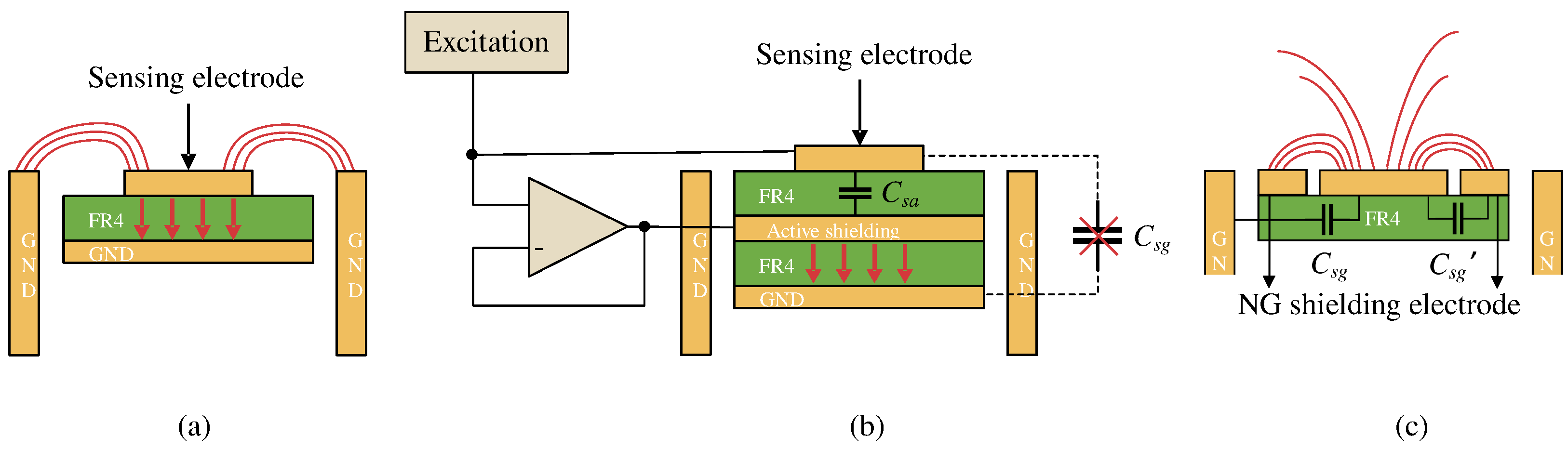
Passive shielding in CPSs is commonly achieved by ensuring that the sensor’s metal housing or other shielding components are properly grounded, thus allowing any interfering currents that do penetrate to be directed to the ground instead of affecting the sensor’s measurement circuitry.
Figure 2a explains the principle of the grounded shielding electrode used in CPSs to shield against external electromagnetic interference. A grounded plate below the sensing electrode isolates it from backside interference, blocking field lines and concentrating the sensing region above. The grounded metal housing shields the system from external interference. While grounding is crucial for noise reduction and signal integrity, it can also couple with sensing electrodes, creating stray capacitance, especially in grounded CPSs. Fringing effects between the sensing electrode and the grounded plate can introduce additional capacitance, leading to reduced sensor sensitivity [
19,
31,
32].
2.2. Active Shielding
Active shielding involves introducing one or more actively generated electric fields around the sensor to counteract or attenuate the effects of external interference. As shown in
Figure 2b, in a CPS, an active shielding electrode is added between the top-layer sensing electrode and the bottom-layer grounded electrode. The excitation signal, after being buffered by an operational amplifier, is directly applied to the active shielding electrode. This ensures that the potential of the active shielding electrode,
, is always equal to the potential of the sensing electrode,
, resulting in a zero potential difference,
. Since the charge stored in the capacitance between the sensing electrode and the active shielding electrode,
Q, is directly proportional to the potential difference
(
), when
is zero, the charge
Q is also zero. This means that the capacitance between the sensing electrode and the active shielding electrode does not store any charge in the measurement circuit, and therefore, has no impact on the charging and discharging process of the measured capacitance
between the sensor and the ground. Consequently, active shielding can effectively eliminate parasitic capacitance caused by the ground plane without reducing the sensor sensitivity [
31]. To effectively implement active shielding, the signals on the shielding and sensor must be in phase, requiring a high-bandwidth amplifier with minimal distortion and propagation delay. However, maintaining identical potentials on these electrodes can be challenging, leading to limitations in cost and power consumption.
2.3. Near-Ground Shielding
In practical applications, the cost, performance, portability, and adaptability of sensors should be taken into consideration comprehensively, so it is necessary to explore and design the suitable working mode, position, and shape of the shielding electrode. To improve the shielding ability and adaptability of CPSs in various operational environment, we propose a new shielding structure, near-ground shielding, for grounded CPSs in this paper.
In fact, near-ground shielding is a passive shielding method. As shown in
Figure 2c, a grounded electrode coplanar and surrounding the sensing electrode was designed to fit between the sensing electrode and the ground ring. This design brings the sensing electrode and the coplanar grounded electrode closer together, concentrating the electric field primarily between the two coplanar electrodes, forming the capacitance
. Since the grounded ring is farther from the sensing electrode, the coupling between them becomes weaker. Both the coplanar grounded electrode and the ground ring are grounded, and the total capacitance to ground becomes
, with electric field lines radiating outward. When a target approaches,
is much larger than
, but since the change in capacitance to the ground is
, it does not affect the sensor sensitivity. This is the concept and principle of near-field shielding.
The proposed shielding electrode is closer to the sensing electrode and separates it from a grounded copper ring, effectively redirecting the electric field lines emanating from the sensing electrode. The sensing electrode and the near-ground shielding electrode develop a planar capacitor. When an object approaches, the capacitance between them will undergo significant changes, ensuring the sensitivity of the sensors. Additionally, since the near-ground electrode is also grounded for shielding, it can effectively shield the interference emanating from metallic surroundings, offering the advantages of easy implementation and low cost as passive shielding. The proposed near-ground shielding structure can also work in active mode by connecting to an operational amplifier, implementing active shielding techniques. The performance of the proposed structure is analyzed and compared in the following sections.
3. Sensor Design and Simulation
3.1. Sensor Models
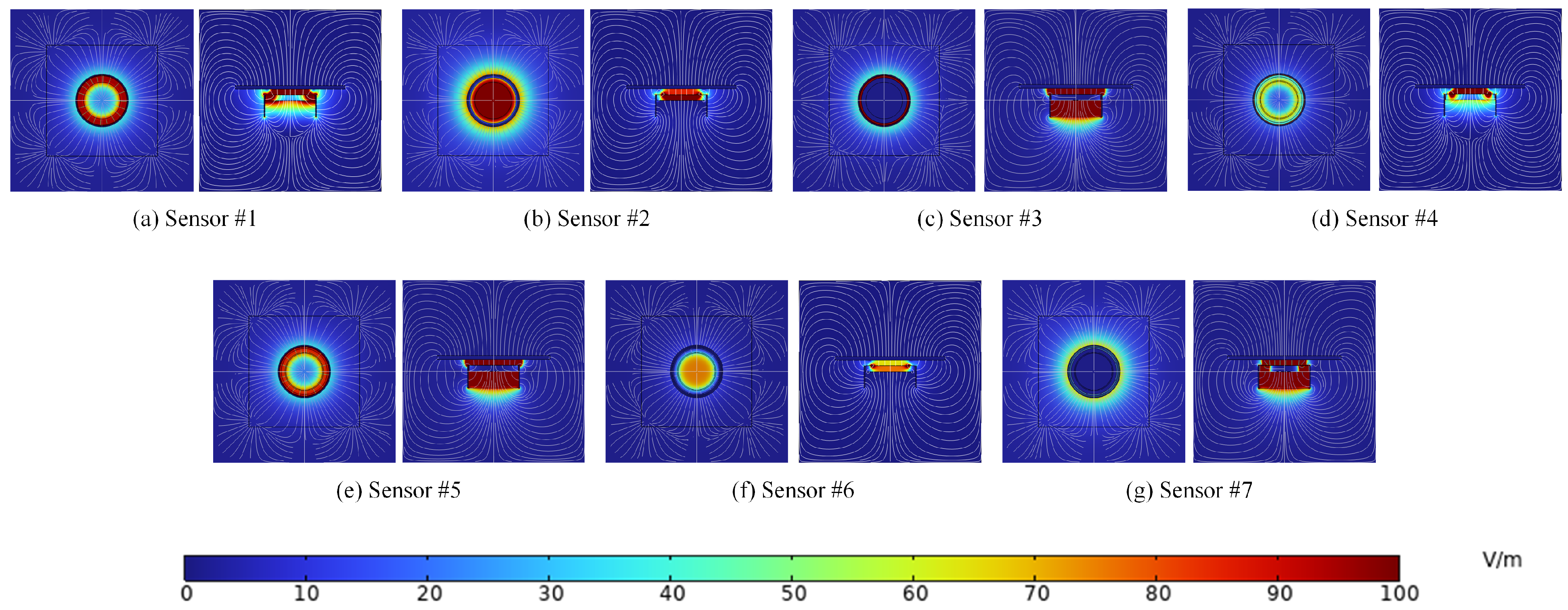
To validate the effectiveness of the proposed near-ground shielding electrode, we conducted a comparative study with a traditional shielding method. Multiple shielding modes, including active, passive, and combinations thereof, were considered in this study. Additionally, the possibility of using multiple shielding electrodes to optimize the shielding performance was explored. It should be noted that if multiple shielding electrodes are all actively shielded, the potentials between the shielding electrodes and the sensing electrode are difficult to maintain synchronously due to the influence of environmental parasitic capacitance, resulting in charge crosstalk between the electrodes and degrading the sensor performance. Therefore, this shielding scheme was excluded from the design. Based on the above design considerations, seven sensor structures that combined different shielding methods were designed and compared in this study.
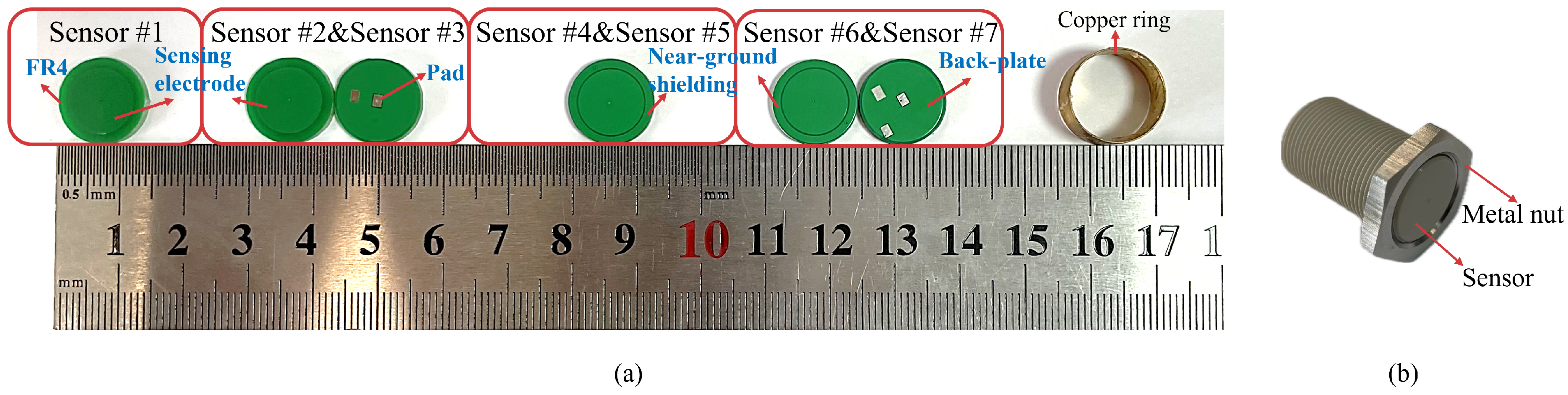
Figure 3 illustrates the seven sensor structures with various shielding modes. Each sensor consisted of a grounded copper ring and a printed circuit board (PCB) with a thickness of 1.6 mm. The sensing electrode and shielding electrode were respectively located on the top or bottom layer of the PCB. The PCB was embedded in the grounded copper ring, with its top layer flush with the edge of the ring. All the copper layers (sensing/shielding electrodes) had a thickness of 35
m.
Table 1 provides the size of every component. The seven sensor structures differed primarily in the configuration of the shielding layer on the PCB, as detailed below.
(1) Sensor #1 (reference sensor): A circular sensing electrode was located on the top layer of the PCB, with a diameter smaller than the PCB itself. There was no shielding layer, which provided a baseline for evaluating the different shielding methods.
(2) Sensor #2 (grounded bottom-layer shielding): Building upon Sensor #1, a grounded circular pad, slightly smaller than the PCB, was added to the bottom layer. This implemented a grounded shielding method.
(3) Sensor #3 (active bottom-layer shielding): similar to Sensor #2, but the circular copper pad on the bottom layer was configured as an active shielding layer by utilizing active shielding techniques.
(4) Sensor #4 (near-ground top-layer shielding): Starting with Sensor #1, a grounded annular copper pad was placed on the top layer and tightly surrounded the sensing electrode. This implemented a near-ground shielding method.
(5) Sensor #5 (active top-layer shielding): similar to Sensor #4, but the annular copper pad on the top layer was configured as an active shielding layer by utilizing active shielding techniques.
(6) Sensor #6 (combined shielding—near-ground top and grounded bottom): Based on Sensor #4, a ground circular copper pad, slightly smaller than the PCB, was added to the bottom layer and configured as a grounded shielding layer. This implemented a combined shielding method with near-ground top-layer shielding and grounded bottom-layer shielding.
(7) Sensor #7 (combined shielding—near-ground top and active bottom): similar to Sensor #6, but the circular copper pad on the bottom layer was configured as a grounded shielding layer by combining top-layer near-ground shielding with bottom-layer active shielding.
3.2. FEM Simulations
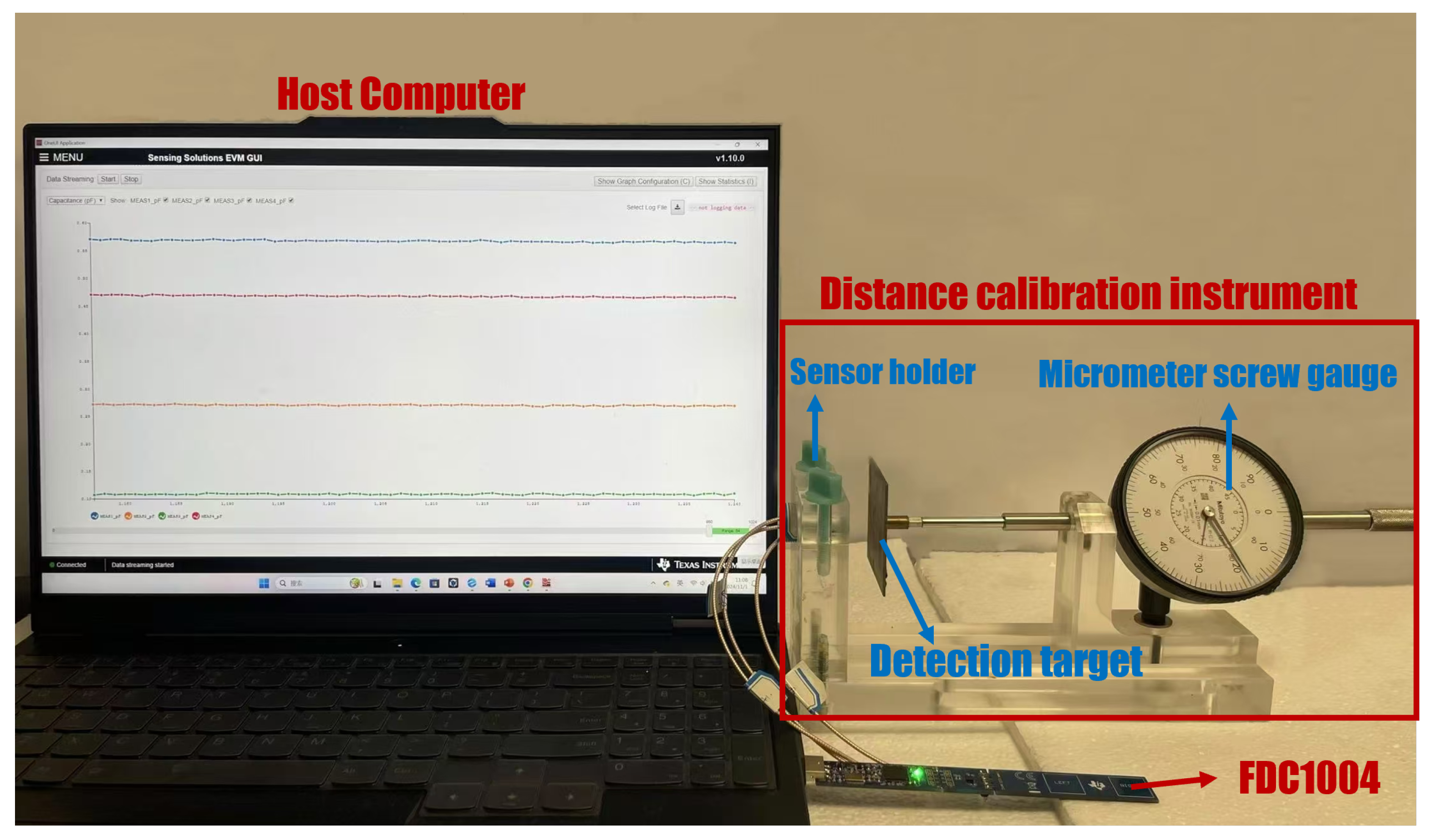
COMSOL Multiphysics is commonly employed for finite element simulation (FEM) to solve for capacitance variations of a sensor electrode as an object approaches it in an electrostatic field. Note that in active shielding, the shielding electrode and the sensing electrode maintain the same potential but are not directly connected. In practical applications, sinusoidal AC signals are commonly used, which is difficult to describe in a static electric field. Therefore, to analyze the electric field and potential distribution under active shielding, it is necessary to establish simulation boundary conditions using an electric current field.
In the simulation models, the sensor used a 1.6 mm thick FR4 substrate (
) with 35
m copper electrodes that are compatible with standard PCB fabrication. The simulation model included a 50 mm × 50 mm × 0.5 mm square copper plate as the conductive target, matching the experimental setup described in
Section 4.1. The distance to target (d) was defined as the perpendicular separation between the target surface and the sensor’s top plane (
Figure 3). All simulations evaluated the capacitance variation across d = 1–45 mm, which was consistent with the experimental measurements.
3.2.1. Simulation Setup for Passive Shielding Method
To simulate the electric field distribution of a capacitive proximity sensor under grounded shielding conditions in COMSOL, Gauss’s law is used to calculate the electric displacement, and the electric field is derived from the electric potential
V. The electrostatic relationship is as follows:
where
V and
are the electric potential on the capacitor plate and space charge density, respectively [
33,
34].
The power system investigated in this study was a multi-conductor system. The sensing electrode and the object to be detected served as voltage terminals, while the shielding electrode was grounded. The capacitance matrix characterized the relationship between the applied voltage and charge on all the electrodes in the system. This matrix was determined experimentally using a steady-state source scanning method by sequentially charging pairs of voltage terminals and given by
where
and
are the total charges on the sensing electrode and detection target, while
and
are their respective ground potential differences.
/
represents the self-capacitance of the sensing electrode or detection target, and
denotes the mutual capacitance between the sensing electrode and the detection target [
35].
3.2.2. Simulation Setup for Active Shielding Method
When simulating active shielding using a static electric field, the independent operation of voltage sources during parameter scanning made it difficult to accurately model the in-phase voltage variation and zero charge transfer between the sensing electrode and the shielding electrode. In contrast, a current field simulation could better model the electromagnetic coupling in active shielding mode, which more accurately reflected the actual situation. The governing electric current conservation equation for the sensing electrode, active shielding electrode, and grounded electrode was given by
where
is the conductivity,
is the displacement current in time-varying fields, and
denotes the time rate of change of the charge density [
36].
Under the aforementioned boundary conditions, the copper ring remained grounded. When the sensing electrode and the active shielding electrode were driven by voltage signals of the same frequency and amplitude, the potential difference between the two electrodes remained constant. Due to this constant potential difference, no charge transfer occurred between the two electrodes in the capacitive system, and thus, had no impact on the overall charge distribution. Furthermore, as the active shielding electrode was in close proximity to the sensing electrode, it effectively reduced the coupling between the system and the external environment. In this current field simulation, the capacitance value was obtained by calculating the admittance:
where Im(
Y) represents the susceptance, which is the imaginary part of the admittance
Y at the two electrode terminals, and
denotes the angular frequency of the AC excitation signal in the capacitive system.
3.2.3. Simulation Results
Figure 4 presents the electric field distributions of the seven sensor structures obtained through electrostatic and current field simulations. For the sensors without a shielding electrode on the bottom PCB (sensors #1, #4, and #5), the electric field intensity was concentrated between the sensing electrode and the ground plane. Adding a grounded shielding electrode to the bottom (sensors #2 and #6) concentrated the electric field, which reduced the induced electric field strength between the top sensing electrode and the ground plane, and consequently decreased the sensor sensitivity. With an active shielding electrode on the bottom (sensors #3 and #7), the electric field between the top and bottom electrodes was nearly zero. However, sensor #7, with an additional top grounded shielding electrode, experienced a capacitance effect between the top and bottom shielding electrodes, which was greater than the edge effect between the top shielding electrode and the sensing electrode. This resulted in a significant reduction in the sensor sensitivity. Sensor #6, with a coplanar grounded shielding electrode, completely isolated the sensing electrode from the ground plane, which led to a significant decrease in the sensor sensitivity.
To achieve the optimal performance of the NG shielding electrode, we investigated the effects of the gap width between the shielding and sensing electrodes on the capacitance value through simulations.
Figure 5 shows the simulated capacitance values of sensor #4 versus the target distance (d) for different gap widths (0.25 mm, 0.5 mm, and 0.75 mm). It can be found from
Figure 5 that the absolute capacitance dropped by 23.7% by making the gap width between the electrodes larger from 0.25 mm to 0.75 mm, where the capacitance variation (
) increased by 10.5%. Thus, the gap width between the NG shielding and sensing electrodes was set as 0.75 mm for the following simulation and experiments.
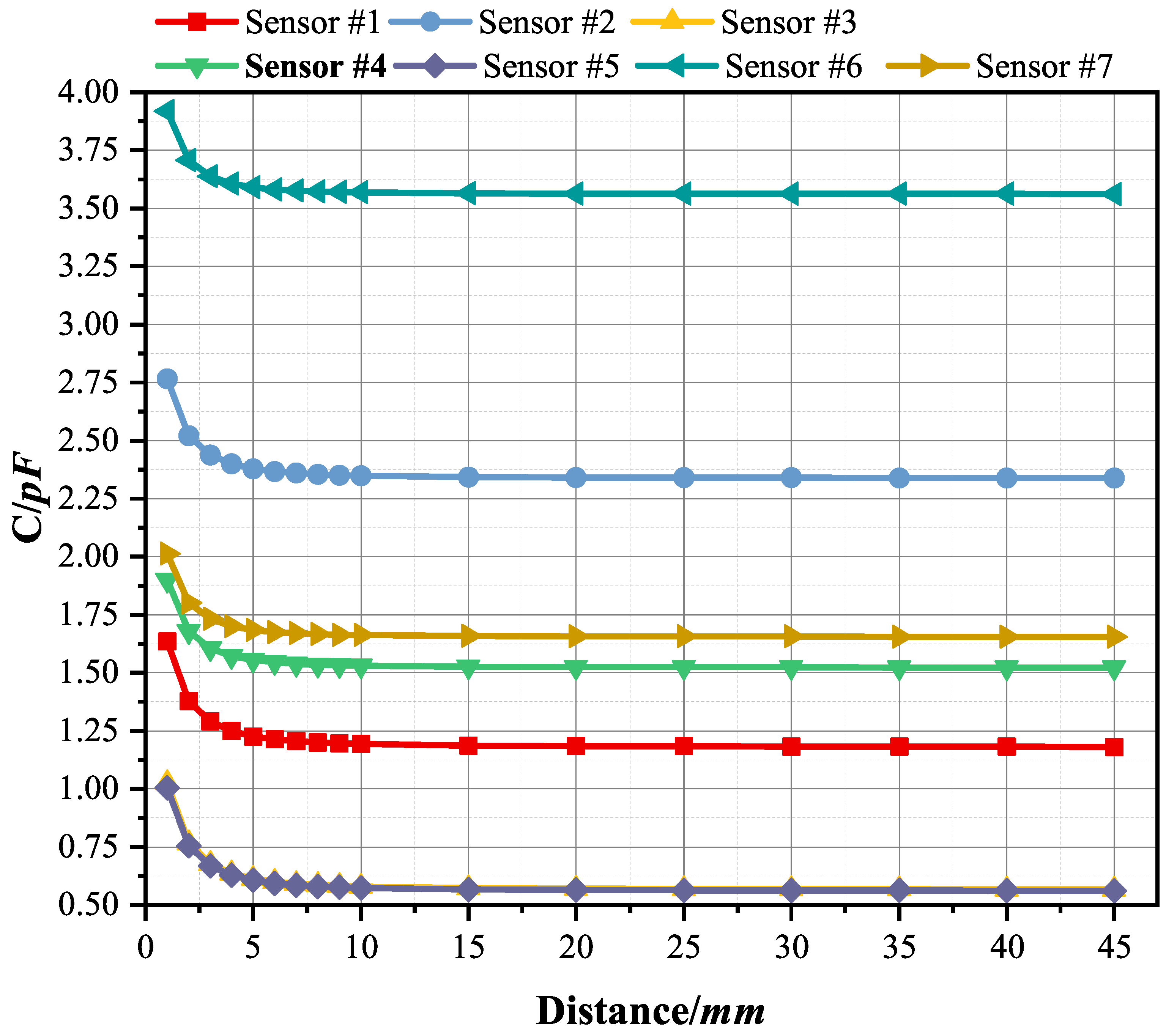
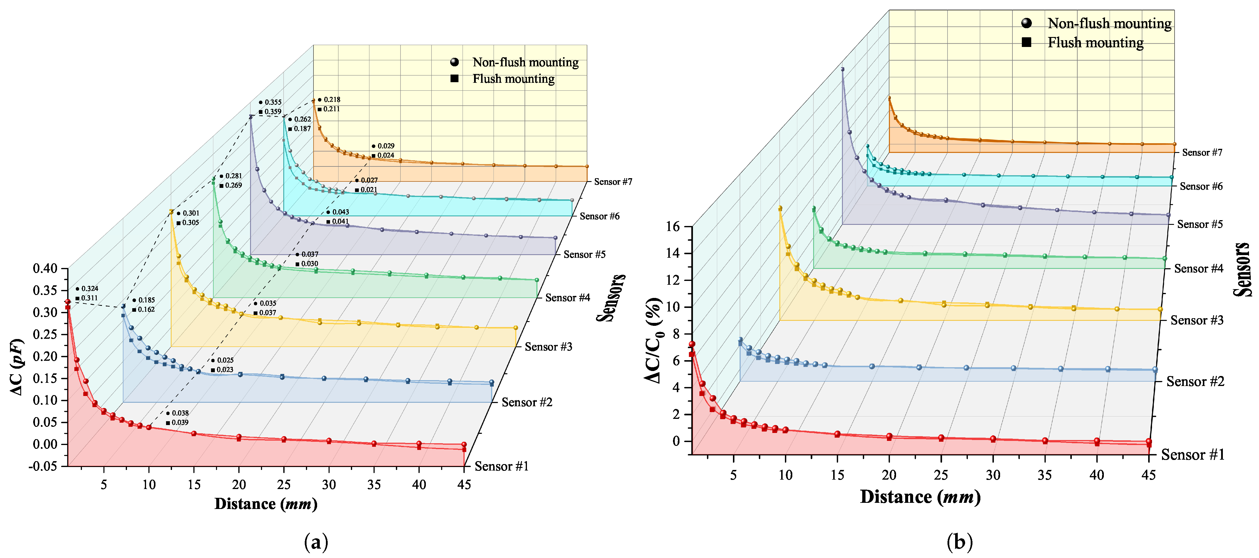
Furthermore, we conducted a parametric sweep of the measurement distance to quantitatively analyze the capacitance and sensitivity of different sensor structures. The measurement distance started from 1 mm and increased in 1 mm increments to 10 mm, followed by 5 mm increments to 45 mm.
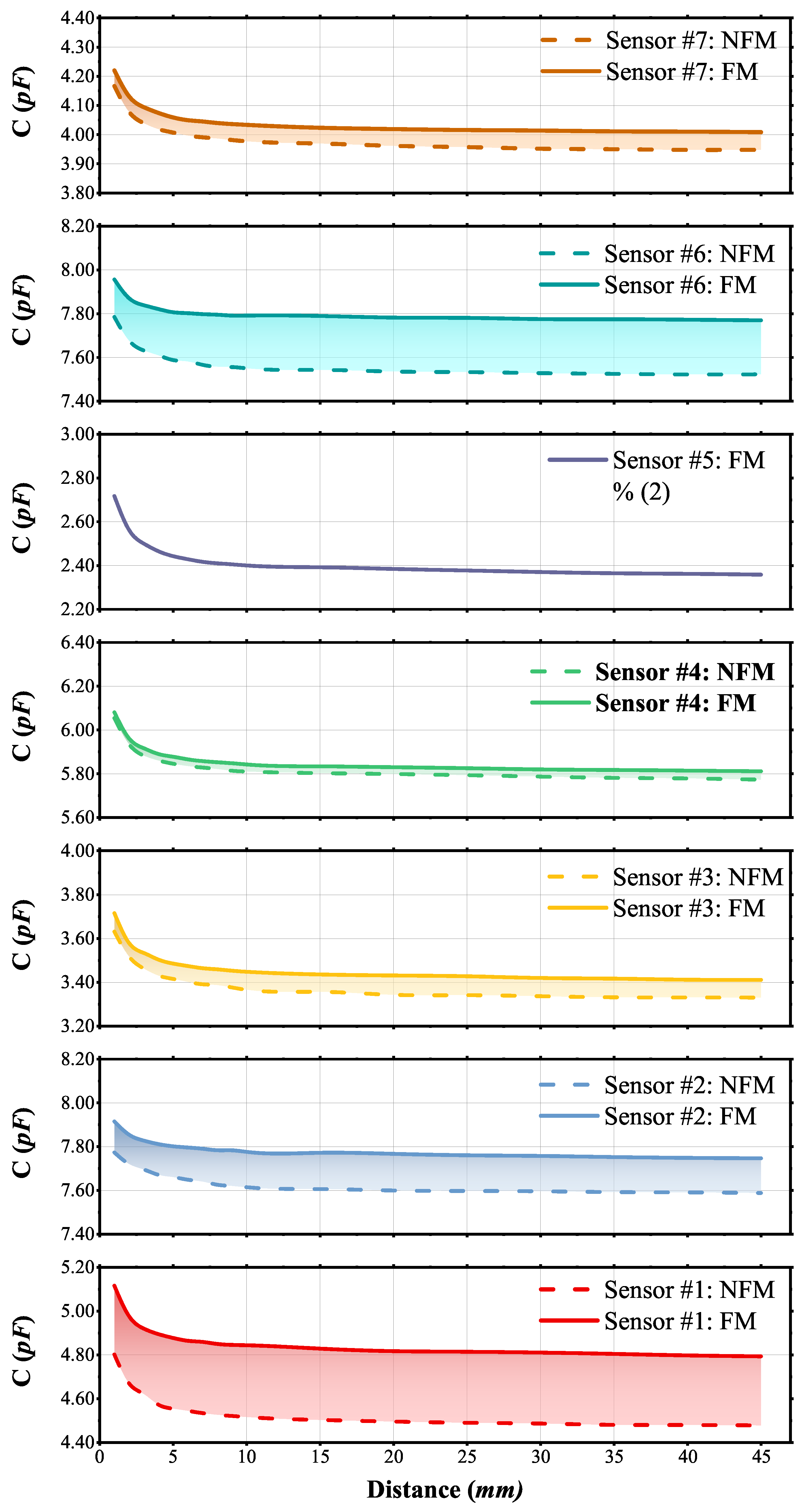
Figure 6 shows the curves of the ground capacitance of each sensor as a function of the measurement distance. The capacitance values of the sensors decreased as the distance between the sensors and the target increased. Compared with the reference sensor (sensor #1), sensors #2, #4, #6, and #7 possessed larger capacitance values due to the extension of area in the grounded electrode. When the target was at a distance of 1 mm from the sensor, the capacitance variation of sensor #1 was about 450 fF, and sensors #2, #4, #6, and #7 diminished the capacitance variation to different extents, meaning lower sensitivities. Sensors #3 and #5 decreased the capacitance values by about 600 fF and keep the capacitance variation close to that of sensor #1.


