Article

Accelerating CRYSTALS-Kyber: High-Speed NTT Design with Optimized Pipelining and Modular Reduction

Computer and Network Engineering Department, Umm Al-Qura University, Makkah 24382, Saudi Arabia
*
Author to whom correspondence should be addressed.
Electronics 2025, 14(11), 2122; https://doi.org/10.3390/electronics14112122
Submission received: 17 April 2025 / Revised: 11 May 2025 / Accepted: 22 May 2025 / Published: 23 May 2025

Abstract

:
The Number Theoretic Transform (NTT) is a cornerstone for efficient polynomial multiplication, which is fundamental to lattice-based cryptographic algorithms such as CRYSTALS-Kyber—a leading candidate in post-quantum cryptography (PQC). However, existing NTT accelerators often rely on integer multiplier-based modular reduction techniques, such as Barrett or Montgomery reduction, which introduce significant computational overhead and hardware resource consumption. These accelerators also lack optimization in unified architectures for forward (FNTT) and inverse (INTT) transformations. Addressing these research gaps, this paper introduces a novel, high-speed NTT accelerator tailored specifically for CRYSTALS-Kyber. The proposed design employs an innovative shift-add modular reduction mechanism, eliminating the need for integer multipliers, thereby reducing critical path delay and enhancing circuit frequency. A unified pipelined butterfly unit, capable of performing FNTT and INTT operations through Cooley–Tukey and Gentleman–Sande configurations, is integrated into the architecture. Additionally, a highly efficient data handling mechanism based on Register banks supports seamless memory access, ensuring continuous and parallel processing. The complete architecture, implemented in Verilog HDL, has been evaluated on FPGA platforms (Virtex-5, Virtex-6, and Virtex-7). Post place-and-route results demonstrate a maximum operating frequency of 261 MHz on Virtex-7, achieving a throughput of 290.69 Kbps—1.45× and 1.24× higher than its performance on Virtex-5 and Virtex-6, respectively. Furthermore, the design boasts an impressive throughput-per-slice metric of 111.63, underscoring its resource efficiency. With a 1.27× reduction in computation time compared to state-of-the-art single butterfly unit-based NTT accelerators, this work establishes a new benchmark in advancing secure and scalable cryptographic hardware solutions.

1. Introduction

Traditional public key cryptographic (PKC) schemes, including (Rivest–Shamir–Adleman) and elliptic-curve cryptography (ECC), derive their security from the computational difficulty of solving problems like integer factorization and the discrete logarithm on elliptic curves [1]. These problems are virtually unsolvable within a reasonable timeframe using classical computing methods. However, quantum computing challenges this premise through algorithms like Shor’s algorithm [2], which efficiently solves these problems, rendering RSA and ECC vulnerable to quantum-based attacks. The urgency of this threat is underscored by advancements such as Google’s 53-qubit quantum processor, which completed a computation in 200 s—equivalent to 10,000 years on a classical supercomputer [3]. With quantum computing architectures rapidly evolving, conventional PKC systems face significant security risks [4]. As a result, developing and standardizing post-quantum cryptographic algorithms is critical to ensuring secure communications in an era dominated by quantum technology.
To counteract the growing security risks posed by quantum computing, the National Institute of Standards and Technology (NIST) launched a groundbreaking standardization initiative for post-quantum cryptography (PQC) in 2017 [5]. This initiative aimed to identify and evaluate cryptographic algorithms capable of resisting quantum-based attacks, ultimately selecting candidates for future cryptographic standards. Following an extensive multi-year evaluation process, NIST announced in 2024 the final selection of four algorithms for standardization: CRYSTALS-Kyber [6], CRYSTALS-Dilithium [7], Falcon [8], and SPHINCS+ [9]. Among these, SPHINCS+ employs a hash-based construction for digital signatures, while the remaining three algorithms rely on lattice-based cryptographic techniques. Lattice-based methods are particularly esteemed for their strong security guarantees and computational efficiency, making them highly suitable for diverse cryptographic applications [10,11].

1.1. Motivation for CRYSTALS-Kyber and the Importance of Hardware-Optimized Number Theoretic Transform

Among the lattice-based methods, CRYSTALS-Kyber [6], selected as the primary key encapsulation mechanism (KEM) in the PQC standardization process, distinguishes itself through a combination of robust security, computational simplicity, and adaptability to constrained environments. At its core, Kyber relies on efficient and parallelizable polynomial operations facilitated by the Number Theoretic Transform (NTT), a fundamental component of lattice-based cryptographic algorithms [10]. Additionally, its deterministic structure and compact ciphertext sizes enhance compatibility with hardware accelerators, positioning CRYSTALS-Kyber as a leading candidate for high-speed cryptographic solutions.
Beyond its critical role in cryptographic algorithms like CRYSTALS-Kyber and other lattice-based PQC schemes, the NTT also serves as a versatile computational tool across multiple domains. Its ability to efficiently perform polynomial convolution in the frequency domain makes NTT hardware accelerators indispensable in areas such as network processing [12], image compression and processing [13,14], and error correction codes [15,16]. These diverse applications underscore the wide-ranging utility of NTT, particularly in high-performance computing environments.
The motivation for implementing NTT in hardware stems from its inherently parallelizable computations, including forward (FNTT) and inverse (INTT) transformations based on Cooley–Tukey and Gentleman–Sande butterfly structures. These computations benefit significantly from dedicated hardware accelerators, such as field-programmable gate arrays (FPGAs) and application-specific integrated circuits (ASICs). By employing multiple architectural techniques, hardware implementations of NTT achieve remarkable improvements in computational throughput and latency, while also addressing critical constraints like area efficiency and power consumption. These advancements not only ensure cryptographic resilience but also enhance the computational performance required to meet the demanding needs of modern high-performance applications across diverse domains.

1.2. Advances in NTT Hardware Accelerators: Enhancing Efficiency and Flexibility for CRYSTALS-Kyber and Beyond

Several hardware accelerators have been developed to enhance the efficiency of Number Theoretic Transform (NTT) computations, which play a critical role in lattice-based cryptographic algorithms like CRYSTALS-Kyber.
Single Butterfly Unit Implementations: One of the commonly adopted approaches involves a ping-pong memory access scheme combined with a single butterfly unit design iteratively. Notable examples of such architectures are found in [17,18,19,20]. In [17], a modular multiplication technique is introduced for CRYSTALS-Kyber’s FNTT and INTT operations, utilizing parameters n = 256 , q = 3329 , and  k = 2 . This implementation achieves an FNTT and INTT computation within 490 clock cycles on a Xilinx Artix-7 FPGA, operating at 257 MHz, and requiring only 1.9  μ s. On the other hand, the modular multiplication technique in [18] employs parameters n = 256 , q = 7681 , and  k = 2 , completing FNTT/INTT computations in 1024 clock cycles with an operating frequency of 136 MHz and a total computation time of 7.5  μ s. In addition to the modular multiplication design, the work in [19] exclusively targets FNTT operations, adopting a serial hardware accelerator with register banks to minimize resource usage while maintaining computational efficiency. Meanwhile, the architecture proposed in [20] utilizes a ping-pong memory access scheme to illustrate the advantages of unified and dedicated butterfly designs—Cooley–Tukey and Gentleman–Sande configurations—for both FNTT and INTT implementations
High-Speed NTT Accelerators: These accelerators have been extensively explored in the literature [21,22,23,24], with notable designs addressing challenges in memory efficiency and computational latency. In [21], a high-speed memory-efficient NTT implementation is presented using parameters similar to [17]. This design completes FNTT and INTT computations in 7725 and 9347 clock cycles, respectively. A reconfigurable high-speed multi-Butterfly configuration architecture in [22] employs a 2 × 2 butterfly core, merging two levels of FNTT/INTT operations. This architecture integrates four butterfly units, each consisting of modules for multiplication, modular reduction, addition, and subtraction. Pipeline registers optimize latency, while a one-bit m o d e signal toggles between FNTT and INTT operations. With CRYSTALS-Kyber parameters n = 256 and q = 3329 , this design achieves an operating frequency of 222 MHz on an Artix-7 FPGA, requiring 324 clock cycles per computation. A more resource-intensive design is found in [23], where 16 butterfly units are utilized to significantly reduce clock cycles and computation time for both FNTT and INTT operations. The most recent design, presented in 2024 [24], utilizes 64 butterfly units to achieve a low-latency NTT accelerator, substantially decreasing the number of clock cycles required for FNTT and INTT computations.
Enhancing Speed and Area Efficiency: The study in [25] presents high-performance NTT hardware accelerators designed to achieve low complexity and high-speed processing. This is accomplished through the use of a pipelined Montgomery reduction unit, which enables efficient modular multiplication. To further optimize area efficiency, the design incorporates a precalculation strategy, significantly reducing hardware resource consumption. Additionally, the implementation leverages a block-based storage method, which enhances data management and improves overall performance, making it well-suited for computationally intensive tasks.
Flexible and Adaptable NTT Architectures: Most existing NTT hardware accelerators dedicated to CRYSTALS-Kyber [17,18,19,20,21,23,24,25] exhibit limited flexibility, restricting their adaptability to varying cryptographic parameters. To address this limitation, the work in [26] introduces a flexible, parameterized architecture capable of generating adaptable NTT-based polynomial multipliers. These multipliers are designed to accommodate a broad range of lattice-based cryptographic parameters in PQC, employing a unified butterfly unit to perform FNTT and INTT computations. The architecture dynamically generates NTT multipliers based on input parameters, optimizing both throughput and area utilization to meet diverse application requirements. In addition to the parameterized multiplier approach of [26], the study in [27] proposes an FPGA-based configurable NTT architecture capable of supporting six distinct parameter sets relevant to homomorphic encryption and post-quantum cryptographic schemes. Additionally, a recent contribution in [28] presents a flexible and parallel NTT hardware accelerator, further enhancing adaptability in cryptographic hardware designs.
Open-Source Tools and Resources: Beyond CRYSTALS-Kyber-specific implementations, open-source polynomial multiplication tools have emerged as valuable resources. NFLlib, described in [29], is a C++ library tailored for ideal lattice cryptography, offering optimized NTT computations at the algorithmic level. Another notable tool, TTech-LIB, introduced in [30], generates Verilog hardware descriptions for various polynomial multiplication architectures. The implementation results for TTech-LIB are further detailed in [29]. Furthermore, the Verilog HDL implementations of NTT accelerators presented in [26,27] are made available as open-source resources.
These advancements underscore the ongoing efforts to enhance flexibility, efficiency, and adaptability in NTT hardware accelerators, catering to the evolving demands of post-quantum and homomorphic cryptographic applications.

1.3. Limitations in Existing NTT Accelerator Designs: Challenges and Opportunities for Improvement

Despite significant advancements in NTT accelerator designs, as discussed in Section 1.2, several limitations persist, hindering the performance of cryptographic systems in high-speed applications:
Modular Reduction Efficiency: Current NTT accelerators [17,18,19,20,21,23,24,31] predominantly use Barrett or Montgomery modular reduction techniques, which rely on integer multipliers. Although effective, these methods introduce higher critical path delays and inflate hardware resource utilization, particularly in terms of digital signal processors (DSPs). This compromises circuit operating frequencies, reducing the overall performance efficiency of cryptographic computations.
Unified Butterfly Architecture Optimization: While unified architectures employing Cooley–Tukey and Gentleman–Sande butterfly structures exist, they lack sufficient optimization to minimize computation time and enhance throughput [19,20,26,27,31]. These designs fail to fully exploit pipelining techniques to address bottlenecks in latency and resource efficiency.
Hardware Resource Utilization: Existing accelerators demonstrate significant overhead in hardware resources (slices, LUTs, and FFs), which makes them less suited for scalable deployment on modern FPGA devices.
Flexibility in Parameter Adaptation: Most designs are limited in their flexibility, making them unsuitable for adapting to varying cryptographic parameters required in diverse PQC applications.

1.4. Proposed High-Speed NTT Accelerator for CRYSTALS-Kyber: Innovations in Modular Reduction and Pipelining

To address these challenges, the article introduces an innovative and efficient NTT accelerator architecture tailored specifically for CRYSTALS-Kyber. The proposed design integrates several key advancements:
  • Optimized Barrett Reduction Architecture with Shift-Add Operations: The modular reduction operation is redesigned to eliminate integer multipliers, replacing them with lightweight shift-add circuits. This novel approach significantly reduces the critical path delay and minimizes hardware resource utilization while enhancing circuit operating frequencies. By eliminating DSP dependency, the architecture achieves greater area efficiency on FPGA devices. Details are in Section 3.3.
  • Pipelined Unified Butterfly Unit Architecture: A dual-stage pipelined butterfly unit is designed to perform both forward NTT (FNTT) and inverse NTT (INTT) computations within a single framework, employing Cooley–Tukey and Gentleman–Sande configurations. This design improves computational throughput, reduces processing latency, and optimizes memory access for efficient data flow. The corresponding details are given in Section 3.2.
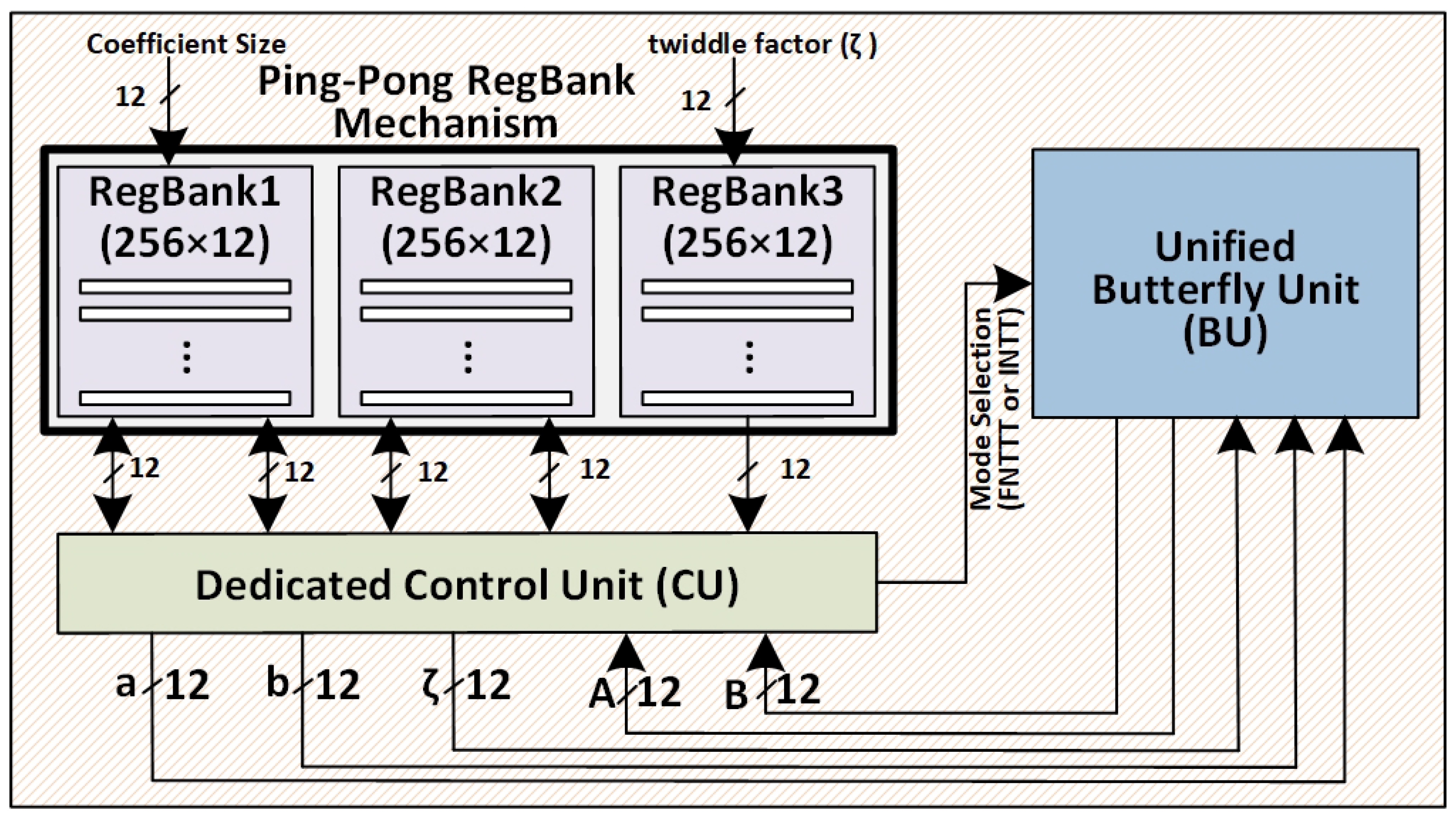
  • Integration of RegBanks for Continuous Data Processing: Three register banks (RegBanks) are utilized to manage input, intermediate, and precomputed data, enabling seamless ping-pong memory access and eliminating idle cycles. This mechanism ensures parallel processing and supports scalable computations (see Section 3).
  • Performance Evaluation and Benchmarking: The proposed NTT accelerator architecture has been implemented in Verilog HDL and synthesized using Vivado v.2023. Performance evaluations were conducted on three FPGA platforms: Virtex-5, Virtex-6, and Virtex-7, with detailed resource utilization reported as follows: 2604 slices, 7141 LUTs, and 7332 FFs for Virtex-5; 2865 slices, 7856 LUTs, and 8066 FFs for Virtex-6; and 3152 slices, 8642 LUTs, and 8873 FFs for Virtex-7. The accelerator executes FNTT and INTT computations within 898 clock cycles, excluding coefficient loading into or from memories. In terms of operating frequency, the Virtex-7 implementation achieves significant speed improvements, operating at 261 MHz, compared to 179 MHz and 209 MHz on Virtex-5 and Virtex-6, respectively. This results in a computation time that is 1.45× faster than Virtex-5 and 1.24× faster than Virtex-6. Similarly, throughput evaluations reveal that the Virtex-7 achieves a remarkable value of 290.69 Kbps, which is 1.45× higher than Virtex-5 and 1.24× higher than Virtex-6. Notably, the Virtex-7 design delivers the highest throughput-per-slice metric of 111.63, emphasizing its efficiency in resource utilization for FNTT and INTT computations. These results underscore the superior performance of the proposed accelerator architecture, making it highly effective for high-speed cryptographic applications (details are in Section 4).
This paper is structured as follows: Section 2 outlines the mathematical foundations necessary to understand the proposed methodology. The architectural design of the NTT-based polynomial multiplication accelerator, along with its innovative features, is detailed in Section 3. The implementation and performance analysis of the proposed accelerator are covered extensively in Section 4. Lastly, Section 5 provides a summary of the findings and discusses their importance in the context of high-speed cryptographic systems .

2. Mathematical Background

Polynomial multiplication forms the computational backbone of CRYSTALS-Kyber, where the NTT is the most resource-intensive component. Conceptually, NTT is similar to the Discrete Fourier Transform (DFT). The NTT operates over a finite field Z q , in contrast to the complex domain used in the DFT. Given a polynomial f ( x ) = i = 0 n 1 f i x i of degree n 1 , its transformation into the NTT domain is expressed in Equation  (1).
FNTT = f ^ = N T T ( f ) = i = 0 n 1 f ^ i x i
Here, each coefficient f ^ i is computed as f ^ i = j = 0 n 1 f j ζ ( 2 i + 1 ) · j , where ζ represents a primitive 2 n -th root of unity in Z q . The corresponding inverse transformation is defined in Equation (2).
INTT = f = N T T 1 ( f ^ ) = i = 0 n 1 f i x i
The inverse coefficient computation is given by f i = n 1 j = 0 n 1 f ^ j ζ i ( 2 j + 1 ) , where n 1 is the modular inverse of n in Z q . Both FNTT and INTT are typically implemented using efficient butterfly structures. The Cooley–Tukey (CT-BU) and Gentleman–Sande (GS-BU) butterfly units, applied in a bottom-up fashion, serve the forward and inverse transforms, respectively. Their mathematical formulations are outlined in Equations (3) and (4).
CT - BU : ( a + b ζ ) mod q & ( a b ζ ) mod q
GS - BU : ( a + b ) mod q & ζ ( a b ) mod q
The implementation of the butterfly operations of CT-BU and GS-BU is integrated into an iterative NTT algorithm, as outlined in Algorithm 1. In this algorithm, lines 6 through 11 correspond to the FNTT computation governed by Equation (3). Similarly, to perform INTT, the expressions in Equation (4) can replace the corresponding lines. The remaining steps of the algorithm handle initialization and memory addressing logic for read and write operations.
Algorithm 1 Iterative NTT Algorithm [31]
Input: 
An n-element vector x = [ x 0 , , x n 1 ] w h e r e x i [ 0 , q 1 ]
Input: 
n (power of 2), modulus q  ( q 1 ( m o d 2 n ) )
Input: 
g (pre-computed table of 2n-th roots of unity, bit-reversed order)
Output: 
x N T T ( x )
 1:
  t n / 2 ; m 1
 2:
 while  ( m < n )  do
 3:
     k 0
 4:
    for  ( i 0 ; i < m ; i i + 1 )  do
 5:
       w g [ m + i ]
 6:
      for  ( j k ; j < k ; j j + 1 )  do
 7:
          a x [ j ] {Butterfly starts}
 8:
          b x [ j + t ] · w
 9:
          x [ j ] a + b
10:
         x [ j + t ] a b {Butterfly ends}
11:
     end for
12:
      k k + 2 t ;
13:
   end for
14:
    t t / 2 ; m 2 m
15:
end while

3. Proposed NTT Architecture

The block diagram of the proposed NTT architecture is depicted in Figure 1. It features three Register Banks (RegBanks) designed to store the initial, intermediate, and final results. These RegBanks interface with a butterfly unit through a dedicated control unit. For simplicity, the figure does not display the input and output signals of the NTT core. Further details are provided below.

3.1. Ping-Pong RegBank Mechanism for Parallel FNTT and INTT Processing

As depicted in Figure 1, the architecture incorporates three RegBanks: (i) RegBank1, (ii) RegBank2, and (iii) RegBank3. These RegBanks are integral to efficiently managing the data flow required for both FNTT and INTT computations. Each RegBank has dimensions of 256 × 12 , where 256 corresponds to the total number of addresses, and 12 denotes the size of the CRYSTALS-Kyber coefficient (i.e., the number of bits stored at each address).
RegBank1 and RegBank2: They operate in a ping-pong manner to ensure efficient and uninterrupted data processing. While one RegBank actively delivers input data to the butterfly unit, the other simultaneously stores the computed results. This dual-role mechanism eliminates idle cycles and supports parallel processing, particularly when multiple butterfly units are utilized. Such an approach significantly enhances the overall performance of the FNTT and INTT computations.
RegBank3: It is dedicated to storing the precomputed twiddle factors ( ζ ) necessary for the FNTT and INTT stages. These twiddle factors are crucial for the computations performed at each stage of the transform. Similar to the other RegBanks, RegBank3 is sized 256 × 12 , with the first 128 addresses containing ζ values for the FNTT computation and the remaining 128 addresses holding ζ values for the INTT computation. This optimized utilization of the RegBanks ensures efficient and continuous data flow throughout the computational process.

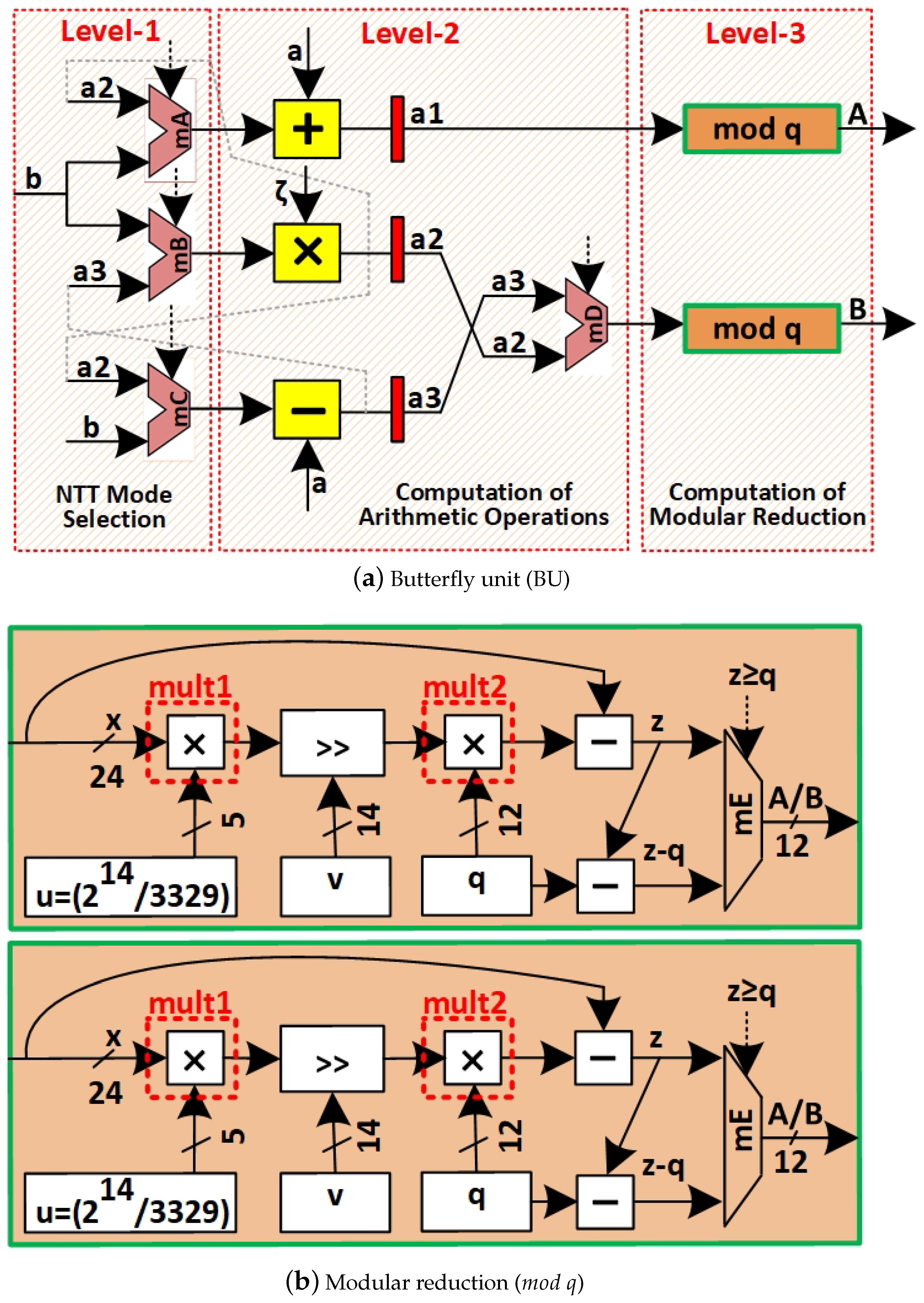
3.2. Unified Butterfly Unit (BU)

The architecture of the proposed unified butterfly unit, as presented in Figure 2, is designed to compute the four mathematical expressions defined in Equations (3) and (4). The unit’s input/output interface features three 12-bit inputs (a, b, and  ζ ) and two 12-bit outputs (A and B). To streamline the diagram’s clarity, the clk and rst signals, as well as other associated control signals, are omitted from Figure 2. This ensures a focused representation of the key computational elements.
Arithmetic and Modular Reduction Units: As illustrated in Figure 2a, the design incorporates three arithmetic operators in level 2: (i) one adder, (ii) one multiplier, and (iii) one subtractor. Additionally, two modular reduction units ( m o d q ) are required in level 3. The arithmetic operators—adder, subtractor, and multiplier—are implemented using the Verilog operators +, −, and ×, respectively. It is important to note that the HDL × operator performs integer multiplication rather than modular multiplication. Modular reduction ( m o d q ), on the other hand, is achieved using the Barrett-based reduction method, which will be discussed later in Section 3.3.
Multiplexers: In addition to the arithmetic and modular reduction units, the unified butterfly unit design shown in Figure 2a includes four 2 × 1 multiplexers: mA, mB, mC, and mD. These multiplexers share a common control signal. When the control signal is set to “0”, the circuit generates results for ( a + b ζ ) m o d q and ( a b ζ ) m o d q , as defined in Equation (3), to perform the FNTT computation. Conversely, when the control signal is set to “1”, the circuit produces results for ( a + b ) m o d q and ζ ( a b ) m o d q , as described in Equation (4), to carry out the INTT computation.
Pipeline Registers: The red-filled vertical bars positioned after each adder, multiplier, and subtractor in Figure 2a represent pipeline registers. These registers reduce the critical path length and enhance the circuit’s operating frequency. Their placement after each arithmetic unit facilitates a two-stage pipeline design for the butterfly unit. As a result, the read address must be generated in the first cycle, while the computed result is stored back in the subsequent cycle. This arrangement ensures efficient processing and improves performance by optimizing the critical path and enabling pipeline operation.

3.3. Optimized Barrett Reduction: Shift-Add Circuits and Architectural Design

The Barrett reduction optimizes modular reduction by replacing costly division operations with more efficient integer multiplications. This approach maps the product of two integers back to Z q . The general Barrett reduction algorithm for computing the reduced product modulo m o d q can be computed using Algorithm 2.
Algorithm 2 General Barrett reduction Algorithm (taken from [19])
Input: 
x (integer), modulus q
Output: 
r = x mod q
1:
Precompute:  μ = 2 k / q , where k is chosen based on bit-width of x
2:
Compute approximate quotient:  t ( x × μ ) k             {mult1 in Figure 2}
3:
Compute t × q : q _ t i m e s _ t q × t                                     {mult2 in Figure 2}
4:
r x q _ t i m e s _ t
5:
if  r q  then
6:
    r r q
7:
end if
Shift-Add Circuit Design for Constant Multiplications in Barrett Reduction: As described in Algorithm 2, implementing Barrett-based modular reduction involves two integer multiplications: one in line 2 and another in line 3 of the algorithm. According to [20], these multiplications require two integer multipliers, which collectively utilize four digital signal processor (DSP) blocks. On 7-series FPGA devices, each DSP block consumes 100 slices, significantly increasing hardware resource requirements. The multiplications in lines 2 and 3 involve constants, making them suitable for optimization. In line 2, the multiplication x × μ involves a precomputed constant μ = 2 k q . Similarly, in line 3, the multiplication q × t also uses the constant q. These constant multiplications can be replaced with a shift-add circuit, eliminating the need for DSP blocks and significantly reducing FPGA slice usage.
Architecture for Barrett Reduction Computations: The architecture implementing Algorithm 3 is depicted in Figure 2b, with mult1 and mult2 marked using red-dashed lines. The mult1 unit performs the arithmetic operations specified in line 2 of Algorithm 3, while mult2 handles the operations from line 3. To compute the resultant coefficient, line 4 utilizes a subtractor unit, ensuring the result remains less than q. Additionally, the conditional subtraction in the if statement of Algorithm 3 is executed whenever the resultant coefficient exceeds q, ensuring it falls within the desired range of <q. This arrangement simplifies and optimizes the modular reduction process.
Algorithm 3 Optimized Barrett reduction algorithm for CRYSTALS-Kyber
Input: 
x (integer), modulus q
Output: 
r = x mod q
1:
Precompute:  μ = 2 14 / 3329 = 5
2:
Compute approximate quotient using shift-add:  t ( ( x 2 ) + x ) 14
3:
Compute t × q using shift-add:  q _ t i m e s _ t ( t 11 ) + ( t 8 ) + ( t 5 ) + t
4:
r x q _ t i m e s _ t
5:
if  r q  then
6:
    r r q
7:
end if

3.4. Efficient Addressing and Signal Management Through an FSM-Based Control Unit

A finite-state machine (FSM)-based controller is employed to manage the control functionality. This controller manages key tasks, such as generating read and write addresses for the Register Banks during computations. Additionally, it provides the appropriate control signals for the routing multiplexers illustrated in Figure 2a,b, enabling the execution of either the FNTT or INTT operations. These operations are performed iteratively, as described in Algorithm 1, with only a single butterfly unit involved in the computation. The control unit plays a pivotal role in efficiently managing the loop counters and coordinating butterfly operations to ensure seamless implementation of Algorithm 1.
Beyond generating control signals, the controller determines the total clock cycles required to implement Algorithm 1. Specifically:
  • Initial data loading: To load 256 input coefficients for the FNTT or INTT computations, a total of 256 clock cycles is required—one cycle per coefficient.
  • Processing stages: For CRYSTALS-Kyber, which entails l o g 2 ( n ) 1 stages (where n = 256 ), the computations require 896 clock cycles. An additional 2 clock cycles account for the pipeline registers—one for filling and one for clearing the pipeline—bringing the total to 898 clock cycles for these stages.
The normalization step, corresponding to the n 1 operation in Equation (4), is integrated into the final stage of the INTT computation. By incorporating it within the existing pipeline, the design eliminates the need for additional clock cycles to perform this operation. After completing the FNTT or INTT computation, an additional 256 clock cycles are required to transfer data from the RegBanks to the design’s output pins. In summary:
  • Initial data loading: 256 cycles
  • Processing (FNTT or INTT): 898 cycles
  • Data transfer to output pins: 256 cycles
The entire process—comprising data loading, FNTT or INTT computation, and data transfer—requires a total of 1410 clock cycles. This well-optimized pipeline design ensures efficient execution and smooth processing within the specified architectural framework.

4. Implementation Results and Comparisons

This section presents the implementation results and comparisons. The performance outcomes of the NTT accelerator are detailed in Section 4.1, while Section 4.2 provides a comparative analysis with state-of-the-art approaches.

4.1. Implementation Results

The implementation results are presented for Virtex-5, Virtex-6, and Virtex-7 FPGA devices in Table 1. It is worth noting that we intend to implement the proposed accelerator on ASIC processing nodes in the future. For the FPGA demonstrations discussed in this article, the area results are reported without utilizing DSPs and Block-RAMs. Column one of Table 1 specifies the implemented NTT operation, which can be either FNTT or INTT. Columns two to four outline the hardware resources utilized by the accelerator, including slices, look-up tables (LUTs), and flip-flops (FFs). Timing results are detailed in columns five to seven, covering clock cycles (CCs), operating frequency (Freq in MHz), and computation time for a single FNTT or INTT process (Latency in μ s), with the computation time determined using Equation (5). Column eight presents the throughput (TP in Kbps), calculated as per Equation (6), while the final column provides the ratio of throughput to slices, as determined by Equation (7).
L a t e n c y ( μ s ) = C l o c k C y c l e s F r e q u e n c y ( MHz )
T h r o u g h p u t ( bps ) = 1 L a t e n c y ( μ s ) = 10 6 L a t e n c y ( s )
T h r o u g h p u t A r e a = T h r o u g h p u t F P G A S l i c e s
The hardware resources utilized by our accelerator, measured in terms of FPGA slices, LUTs, and FFs, are as follows: 2604 slices, 7141 LUTs, and 7332 FFs on the Virtex-5; 2865 slices, 7856 LUTs, and 8066 FFs on the Virtex-6; and 3152 slices, 8642 LUTs, and 8873 FFs on the Virtex-7, as summarized in Table 1. These results indicate a reduction in the number of slices, LUTs, and FFs when transitioning from the Virtex-5 and Virtex-6 to the more advanced Virtex-7 FPGA devices. This performance variation is influenced by several factors. Firstly, the advanced process technology of the Virtex-7 (28 nm) offers higher transistor density and reduced power consumption compared to the 65 nm and 40 nm technologies of Virtex-5 and Virtex-6, respectively, enabling more efficient resource usage and improved performance. Secondly, architectural enhancements in the Virtex-7, such as increased routing efficiency, higher logic density, and improved logic packing, optimize the utilization of slices, LUTs, and FFs. Lastly, advancements in CAD tools for the Virtex-7 further improve resource mapping and utilization by leveraging its modern architecture and process technology. These combined factors contribute to the observed differences in resource usage across the FPGA devices.
The FNTT and INTT computations require 898 clock cycles, excluding the overhead associated with coefficient loading. Further details can be found in Section 3.4. When comparing operating frequencies, the Virtex-7 implementation achieves a speedup of 1.45× (based on the ratio of 261 to 179) and 1.24× (based on the ratio of 261 to 209) over the Virtex-5 and Virtex-6 FPGA devices, respectively. This variation in circuit frequency is primarily attributed to differences in the underlying implementation technologies. As mentioned earlier, the modern Virtex-7 FPGA utilizes a 28nm process technology, while the Virtex-6 and Virtex-5 are fabricated using 40nm and 65nm technologies, respectively. Consequently, the latency for a single FNTT or INTT computation varies across these FPGA platforms due to their differing operating frequencies. Thus, our accelerator architecture implemented on the Virtex-7 FPGA achieves computation times that are 1.45× and 1.24× faster than those on the Virtex-5 and Virtex-6 devices, respectively.
As shown earlier in Equation (6), the throughput is defined as the reciprocal of the computation time, i.e., the latency. Accordingly, the calculated throughput for the FNTT and INTT computations on the Virtex-7 device is 290.69 Kbps, which is approximately 1.45× and 1.24× higher than the throughput values achieved on the Virtex-5 and Virtex-6 devices, respectively. Finally, the last column in Table 1 presents the throughput-per-slice values, which serve as an indicator of the accelerator architecture’s efficiency. A higher throughput-per-slice value reflects both increased throughput and reduced hardware resource utilization. In this context, the Virtex-7 implementation demonstrates the highest throughput-per-slice value of 111.63 for the FNTT and INTT computations, underscoring its superior performance. These results collectively highlight the Virtex-7’s ability to deliver higher throughput while efficiently utilizing fewer hardware resources, further validating its architectural advantages.

4.2. Comparisons to Existing NTT Accelerators

In Table 2, we present a comprehensive comparison of state-of-the-art NTT accelerators. Column one lists the reference designs, while column two specifies the implementation devices. The type of NTT operation, whether FNTT or INTT, is detailed in column three. FPGA area utilization is captured in columns four and five, reporting the number of LUTs and FFs, respectively. Timing information, including clock cycles, circuit frequency (in MHz), and computation time (in μ s), is provided in columns six to eight. Lastly, the final column highlights the number of butterfly units utilized in the NTT accelerators, offering additional insights into their architectural configurations.

4.2.1. Comparison of NTT Accelerators (Single Butterfly Unit)

We begin by comparing our NTT accelerator with RegBanks-based NTT accelerators presented in [19,20]. As shown in Table 2, our accelerator utilizes 7141 LUTs on the Virtex-7 FPGA, compared to 7800 LUTs in [19], demonstrating 1.09× higher efficiency in terms of FPGA LUT utilization. It is worth noting that the reference design in [19] is error-resistant and optimized for space applications, while our design does not consider error-resistance features but supports both FNTT and INTT operations, unlike the reference work, which implements only FNTT. Furthermore, the pipeline registers in the data path of our butterfly unit (Figure 2a) result in a 3.62× higher operating frequency. However, due to limited information in the reference work, a direct comparison of clock cycles and latency is not feasible. Similarly, compared to [20] on the same Virtex-7 FPGA, our NTT accelerator demonstrates 1.30× and 1.28× higher efficiency in LUTs and FFs, respectively. Although the clock cycle requirements of the reference work (898 cycles) match ours, the pipeline registers in our butterfly unit achieve a 13.05× higher operating frequency.
Building on the above comparison, we further evaluate our accelerator against the Artix-7 implementation detailed in [23], which provides additional insights into resource utilization and performance metrics. The Artix-7 implementation in [23], based on a single butterfly unit, uses 948 LUTs and 352 FFs without accounting for the 35 BRAMs. If we compare only LUTs and FFs, the reference work is 7.21× and 19.83× more efficient than our design. However, our accelerator achieves a throughput parity of 1.00× in clock cycles and a 1.37× improvement in operating frequency, resulting in reduced computation time compared to the reference work.
Extending this comparison further, we examine a flexible NTT accelerator presented in [26], which provides additional insights into hardware resource efficiency and performance metrics relative to our design. A flexible NTT accelerator presented in [26] is more efficient in terms of LUTs and FFs, demonstrating 3.35× and 6.40× higher efficiency compared to our Virtex-7 FPGA implementation. This reference design employs 8 DSP blocks, while our work excludes DSP usage. Despite this, our NTT accelerator outperforms in clock cycles, operating frequency, and computation time, as shown in Table 2. Specifically, for FNTT computation, our accelerator achieves 1.02×, 1.50×, and 1.53× higher efficiency in clock cycles, frequency, and latency, respectively, compared to [26]. Similarly, for INTT computation, these efficiency metrics are 1.31×, 1.50×, and 1.97× higher.
Compared to the dedicated NTT accelerator in [28] implemented on the same Virtex-7 FPGA, our design achieves superior performance despite higher LUT and FF usage. Specifically, our accelerator demonstrates 1.28× and 1.42× higher efficiency in clock cycles for FNTT and INTT computations, respectively. Additionally, we achieve 1.04× faster operating frequencies and 1.34× and 1.48× improvements in latency for FNTT and INTT computations, respectively. In [32], a flexible NTT accelerator integrates a RISC-V processor to support operations for various PQC algorithms (CRYSTALS-Kyber, NewHope, and SABER). Compared to the reference NTT core implemented on the ZYNQ-7000 FPGA, our Virtex-7 implementation demonstrates 2.15× and 2.14× higher efficiency in clock cycles for FNTT and INTT computations, respectively. Our implementation also achieves 5.80× faster operating frequencies and 12.50× and 12.46× reductions in latency for FNTT and INTT computations, respectively.
A dedicated NTT accelerator is proposed in [28]. When compared to our implementation on the same Virtex-7 FPGA, their design exhibits lower utilization of LUTs and FFs. Specifically, their architecture is 3.53× and 4.00× more efficient in terms of LUT and FF usage, respectively, as detailed in Table 2. Despite this, our NTT accelerator demonstrates superior efficiency in terms of clock cycles, operating frequency, and overall computation time. For FNTT computation, our design achieves a 1.28× improvement in clock cycle count, a 1.04× higher operating frequency, and a 1.34× reduction in latency compared to the reference design. Similarly, for INTT computation, our accelerator is 1.42× more efficient in clock cycles, 1.04× faster in frequency, and achieves a 1.48× improvement in latency.
In [32], a flexible NTT accelerator is proposed, where flexibility is achieved by integrating an RISC-V processor with the NTT core. The NTT core supports operations for different PQC algorithms: (i) CRYSTALS-Kyber, (ii) NewHope, and (iii) SABER. In contrast, our work is dedicated to CRYSTALS-Kyber NTT. The reference NTT accelerator, implemented on the ZYNQ-7000 FPGA, utilizes fewer LUTs and FFs than our Virtex-7 and Artix-7 implementations, as shown in Table 2. Despite the reduced usage of LUTs and FFs, the reference work incorporates 9 DSP blocks, whereas our design does not use DSPs. Although the reference design is efficient in hardware resource usage, our NTT accelerator demonstrates higher efficiency in clock cycles, operating frequency, and overall computation time on both Virtex-7 and Artix-7 FPGA devices. For comparison, we focus on the Virtex-7 implementation. For FNTT computation, our design achieves a 2.15× improvement in clock cycles, a 5.80× higher operating frequency, and a 12.50× reduction in latency compared to the reference design. Similarly, for INTT computation, our accelerator is 2.14× more efficient in clock cycles, 5.80× faster in frequency, and achieves a 12.46× reduction in latency.

4.2.2. Comparison of NTT Accelerators (Multiple Butterfly Units)

The 2-butterfly unit-based architecture in [17], implemented on an Artix-7 FPGA, achieves 11.23× and 10.90× greater efficiency in LUTs and FFs compared to our single butterfly unit design. However, the reference work requires additional hardware resources, including 2 DSPs and 4 18 KB BRAMs, which are not used in our design. The 2 butterfly units in the reference work provide a 1.81× higher efficiency in clock cycles and computation time, while our NTT accelerator achieves a 0.96× faster operating frequency.
The 4-butterfly unit-based NTT architecture in [23] demonstrates 2.69× and 8.81× higher efficiency in LUTs and FFs compared to our single butterfly unit design. However, the reference work utilizes 35 36 KB BRAMs, which our design does not employ. Despite this, our NTT accelerator achieves a 1.36× faster operating frequency. A 16-butterfly unit-based architecture presented in [23] further demonstrates improved performance in clock cycles and computation time due to its extensive parallelism, although it uses significantly higher hardware resources. In terms of operating frequency, our design is 1.44× faster.
The high-performance NTT accelerator described in [24] incorporates 64 butterfly units with modular adders, subtractors, and multipliers to achieve low computation time. While this reference design is highly efficient in clock cycles and latency due to its extensive parallelism, our single butterfly unit implementation achieves superior operating frequency through pipelining techniques.
Summary of the comparisons: Among the NTT accelerators utilizing a single butterfly unit, as shown in Table 2, the high-speed NTT design with the lowest reported computation time is presented in [23], where the latency for one FNTT and INTT computation is 4.75 μ s. In comparison, our implementation on the identical Artix-7 FPGA achieves a latency of 3.72 μ s for a single FNTT and INTT computation. This makes our NTT accelerator approximately 1.27× faster in terms of computation time compared to the one butterfly unit-based high-speed design reported in [23].

5. Conclusions

In this work, a high-speed NTT accelerator architecture is presented to support polynomial multiplication operations in lattice-based cryptography, with a specific focus on the CRYSTALS-Kyber PQC algorithm. The proposed design incorporates a unified pipelined butterfly unit capable of performing both FNTT and INTT operations, utilizing Cooley–Tukey and Gentleman–Sande configurations. To further enhance performance, a novel Barrett reduction architecture tailored for Kyber is introduced, eliminating the need for integer multipliers by employing shift-add-based modular multiplication. The complete architecture, built around a single butterfly unit and three RegBanks, is implemented in Verilog HDL and evaluated across Virtex-5, Virtex-6, and Virtex-7 FPGA platforms. Post place-and-route results demonstrate that the proposed accelerator achieves a 1.27× reduction in computation time compared to the most efficient single butterfly unit-based NTT design documented in the literature. These findings emphasize the effectiveness of the proposed architecture in addressing the requirements of current and future high-speed cryptographic applications.

Author Contributions

Conceptualization, O.S.S. and M.R.; methodology, A.Y.J. and M.R.; software, A.Y.J.; validation, O.S.S. and M.R.; formal analysis, M.R.; investigation, O.S.S.; resources, M.R.; data curation, A.Y.J.; writing—original draft preparation, O.S.S. and M.R.; writing—review and editing, M.R.; visualization, O.S.S.; supervision, M.R. All authors have read and agreed to the published version of the manuscript.

Funding

This research received no external funding.

Data Availability Statement

Data are contained within the article.

Conflicts of Interest

The authors declare that they have no conflicts of interest.

References

  1. Rashid, M.; Imran, M.; Jafri, A.R.; Al-Somani, T.F. Flexible architectures for cryptographic algorithms—A systematic literature review. J. Circuits Syst. Comput. 2019, 28, 1930003. [Google Scholar] [CrossRef]
  2. Shor, P.W. Polynomial-Time Algorithms for Prime Factorization and Discrete Logarithms on a Quantum Computer. SIAM J. Comput. 1997, 26, 1484–1509. [Google Scholar] [CrossRef]
  3. Arya, K.; Babbush, R.; Bacon, D.; Bardin, J.C.; Barends, R.; Biswas, R.; Boixo, S.; Brandao, F.G.; Buell, D.A.; Burkett, B. Quantum supremacy using a programmable superconducting processor. Nature 2019, 574, 505–510. [Google Scholar] [CrossRef]
  4. Gong, M.; Wang, S.; Zha, C.; Chen, M.C.; Huang, H.L.; Wu, Y.; Zhu, Q.; Zhao, Y.; Li, S.; Guo, S.; et al. Quantum walks on a programmable two-dimensional 62-qubit superconducting processor. Science 2021, 372, 948–952. [Google Scholar] [CrossRef] [PubMed]
  5. National Institute of Standards and Technology. NIST to Standardize Encryption Algorithms That Can Resist Attack by Quantum Computers. Available online: https://csrc.nist.gov/projects/post-quantum-cryptography (accessed on 26 March 2025).
  6. National Institute of Standards and Technology. FIPS 203: Module-Lattice-Based Key-Encapsulation Mechanism Standard. Federal Information Processing Standards Publication. Available online: https://nvlpubs.nist.gov/nistpubs/FIPS/NIST.FIPS.203.ipd.pdf (accessed on 26 March 2025).
  7. National Institute of Standards and Technology. FIPS 204: Module-Lattice-Based Digital Signature Standard. Federal Information Processing Standards Publication. Available online: https://nvlpubs.nist.gov/nistpubs/FIPS/NIST.FIPS.204.ipd.pdf (accessed on 26 March 2025).
  8. Fouque, P.A.; Hoffstein, J.; Kirchner, P.; Lyubashevsky, V.; Pornin, T.; Prest, T.; Ricosset, T.; Seiler, G.; Whyte, W.; Zhang, Z. Falcon: Fast-Fourier Lattice-Based Compact Signatures over NTRU Specifications v1.1. Available online: https://falcon-sign.info (accessed on 26 March 2025).
  9. National Institute of Standards and Technology. FIPS 205: Stateless Hash-Based Digital Signature Standard. Federal Information Processing Standards Publication. Available online: https://nvlpubs.nist.gov/nistpubs/FIPS/NIST.FIPS.205.ipd.pdf (accessed on 26 March 2025).
  10. Imran, M.; Abideen, Z.U.; Pagliarini, S. An Experimental Study of Building Blocks of Lattice-Based NIST Post-Quantum Cryptographic Algorithms. Electronics 2020, 9, 1953. [Google Scholar] [CrossRef]
  11. Rashid, M.; Sonbul, O.S.; Jamal, S.S.; Jaffar, A.Y.; Kakhorov, A. A Pipelined Hardware Design of FNTT and INTT of CRYSTALS-Kyber PQC Algorithm. Information 2024, 16, 17. [Google Scholar] [CrossRef]
  12. Satriawan, A.; Syafalni, I.; Mareta, R.; Anshori, I.; Shalannanda, W.; Barra, A. Conceptual Review on Number Theoretic Transform and Comprehensive Review on Its Implementations. IEEE Access 2023, 11, 70288–70316. [Google Scholar] [CrossRef]
  13. Boussakta, S.; Holt, A.G.J. Number Theoretic Transforms and their Applications in Image Processing. Adv. Imaging Electron. Phys. 1999, 111, 1–90. [Google Scholar]
  14. Zhou, R.; Wen, J.; Zou, Y.; Wang, A.; Hua, J.; Sheng, B. Enhanced image compression method exploiting NTT for internet of thing. Int. J. Circuit Theory Appl. 2023, 51, 1879–1892. [Google Scholar] [CrossRef]
  15. Abdelmonem, M.; Holzbaur, L.; Raddum, H.; Zeh, A. Efficient Error Detection Methods for the Number Theoretic Transforms in Lattice-Based Algorithms. Cryptology ePrint Archive, Paper 2025/170. 2025. Available online: https://eprint.iacr.org/2025/170 (accessed on 21 May 2025).
  16. Brier, E.; Coron, J.S.; Géraud, R.; Maimut, D.; Naccache, D. A Number-Theoretic Error-Correcting Code. arXiv 2015, arXiv:1509.00378. [Google Scholar]
  17. Zhang, C.; Liu, D.; Liu, X.; Zou, X.; Niu, G.; Liu, B.; Jiang, Q. Towards Efficient Hardware Implementation of NTT for Kyber on FPGAs. In Proceedings of the 2021 IEEE International Symposium on Circuits and Systems (ISCAS), Daegu, Republic of Korea, 22–28 May 2021; pp. 1–5. [Google Scholar] [CrossRef]
  18. Chen, Z.; Ma, Y.; Chen, T.; Lin, J.; Jing, J. Towards Efficient Kyber on FPGAs: A Processor for Vector of Polynomials. In Proceedings of the 2020 25th Asia and South Pacific Design Automation Conference (ASP-DAC), Beijing, China, 13–16 January 2020; pp. 247–252. [Google Scholar] [CrossRef]
  19. Khan, S.; Khalid, A.; Rafferty, C.; Shah, Y.A.; O’Neill, M.; Lee, W.K.; Hwang, S.O. Efficient, Error-Resistant NTT Architectures for CRYSTALS-Kyber FPGA Accelerators. In Proceedings of the 2023 IFIP/IEEE 31st International Conference on Very Large Scale Integration (VLSI-SoC), Dubai, United Arab Emirates, 16–18 October 2023; IEEE: New York, NY, USA, 2023; pp. 1–6. [Google Scholar]
  20. Imran, M.; Khan, S.; Khalid, A.; Rafferty, C.; Shah, Y.A.; Pagliarini, S.; Rashid, M.; O’Neill, M. Evaluating NTT/INTT Implementation Styles for Post-Quantum Cryptography. IEEE Embed. Syst. Lett. 2024, 16, 485–488. [Google Scholar] [CrossRef]
  21. Botros, L.; Kannwischer, M.J.; Schwabe, P. Memory-efficient high-speed implementation of Kyber on Cortex-M4. In Proceedings of the Progress in Cryptology—AFRICACRYPT 2019: 11th International Conference on Cryptology in Africa, Rabat, Morocco, 9–11 July 2019; Proceedings 11. Springer: Cham, Switzerland, 2019; pp. 209–228. [Google Scholar]
  22. Bisheh-Niasar, M.; Azarderakhsh, R.; Mozaffari-Kermani, M. High-Speed NTT-based Polynomial Multiplication Accelerator for Post-Quantum Cryptography. In Proceedings of the 2021 IEEE 28th Symposium on Computer Arithmetic (ARITH), Lyngby, Denmark, 14–16 June 2021; pp. 94–101. [Google Scholar] [CrossRef]
  23. Yaman, F.; Mert, A.C.; Öztürk, E.; Savaş, E. A Hardware Accelerator for Polynomial Multiplication Operation of CRYSTALS-KYBER PQC Scheme. In Proceedings of the 2021 Design, Automation & Test in Europe Conference & Exhibition (DATE), Grenoble, France, 1–5 February 2021; pp. 1020–1025. [Google Scholar] [CrossRef]
  24. Saoudi, M.; Kermiche, A.; Benhaddad, O.H.; Guetmi, N.; Allailou, B. Low latency FPGA implementation of NTT for Kyber. Microprocess. Microsyst. 2024, 107, 105059. [Google Scholar] [CrossRef]
  25. Xu, C.; Yu, H.; Xi, W.; Zhu, J.; Chen, C.; Jiang, X. A Polynomial Multiplication Accelerator for Faster Lattice Cipher Algorithm in Security Chip. Electronics 2023, 12, 951. [Google Scholar] [CrossRef]
  26. Derya, K.; Mert, A.C.; Öztürk, E.; Savaş, E. CoHA-NTT: A Configurable Hardware Accelerator for NTT-based Polynomial Multiplication. Microprocess. Microsyst. 2022, 89, 104451. [Google Scholar] [CrossRef]
  27. Mert, A.C.; Öztürk, E.; Savaş, E. FPGA implementation of a run-time configurable NTT-based polynomial multiplication hardware. Microprocess. Microsyst. 2020, 78, 103219. [Google Scholar] [CrossRef]
  28. Rashid, M.; Khan, S.; Sonbul, O.S.; Hwang, S.O. A Flexible and Parallel Hardware Accelerator for Forward and Inverse Number Theoretic Transform. IEEE Access 2024, 12, 181351–181361. [Google Scholar] [CrossRef]
  29. Aguilar-Melchor, C.; Barrier, J.; Guelton, S.; Guinet, A.; Killijian, M.O.; Lepoint, T. NFLlib: NTT-based fast lattice library. In Proceedings of the Cryptographers’ Track at the RSA Conference, San Francisco, CA, USA, 29 February–4 March 2016; Springer: Cham, Switzerland, 2016; pp. 341–356. [Google Scholar]
  30. Imran, M.; Abideen, Z.U.; Pagliarini, S. An open-source library of large integer polynomial multipliers. In Proceedings of the 2021 24th International Symposium on Design and Diagnostics of Electronic Circuits & Systems (DDECS), Vienna, Austria, 7–9 April 2021; IEEE: New York, NY, USA, 2021; pp. 145–150. [Google Scholar]
  31. Aikata, A.; Mert, A.C.; Imran, M.; Pagliarini, S.; Roy, S.S. KaLi: A Crystal for Post-Quantum Security Using Kyber and Dilithium. IEEE Trans. Circuits Syst. I Regul. Pap. 2023, 70, 747–758. [Google Scholar] [CrossRef]
  32. Fritzmann, T.; Sigl, G.; Sepúlveda, J. RISQ-V: Tightly Coupled RISC-V Accelerators for Post-Quantum Cryptography. IACR Trans. Cryptogr. Hardw. Embed. Syst. 2020, 2020, 239–280. [Google Scholar] [CrossRef]
Figure 1. Block Diagram of the Proposed NTT Accelerator Architecture Featuring RegBanks, Unified Butterfly Unit, and Dedicated Control Unit.
Electronics 14 02122 g001
Figure 2. Proposed unified butterfly unit architecture of CT and GS configurations for forward and inverse NTT computations. (a) shows that the design comprises three functional levels: Level-1, Level-2, and Level-3. In Level-1, the control logic determines the computation path based on the selected NTT mode. Multiplexer mB directs the processing flow for FNTT, while multiplexers mA and mC are utilized for INTT execution. Following this, Levels 2 and 3 sequentially perform the necessary arithmetic operations, guided by the selection signals and outputs produced in Level-1. (b) shows the architecture for implementing optimized Barrett reduction algorithm.
Electronics 14 02122 g002
Table 1. Implementation results of our NTT accelerator (after the post-place-and-route) on Xilinx FPGA devices.
DeviceOperationHardware UtilizationsTiming-Related ResultsTPTP/Slices
SlicesLUTsFFsCCsFreq. (MHz)Latency (μs)(Kbps)
Virtex-5FNTT + INTT3152864288738981795.01199.6063.32
Virtex-6FNTT + INTT2865785680668982094.29233.1081.36
Virtex-7FNTT + INTT2604714173328982613.44290.69111.63
Table 2. Comparison to state-of-the-art NTT accelerators. All these architectures, including our NTT accelerator, target n = 256 and q = 3329 parameters.
Designs/YearDeviceNTTHardware AreaTiming-Related ResultsButterfly
TypeLUTsFFsCCsFreq. (MHz)Latency (μs)Units (BUs)
[19]/2023Virtex-7FNTT7800721
[20]/2024Virtex-7FNTT + INTT929894028982044.901
[23]/2021Artix-7FNTT + INTT9483529041904.751
[26]/2022Virtex-7FNTT212811449221745.291
INTT11846.80
[28]/2024Virtex-7FNTT2018182911542504.611
INTT12825.12
[32]/2020ZynQ-7000FNTT2908170193545431
INTT193042.88
[17]/2021Artix-7FNTT + INTT6096404902571.92
[23]/2021Artix-7FNTT + INTT25437922321821.274
[23]/2021Artix-7FNTT + INTT95082684691720.4016
[24]/2024Artix-7FNTT18,29612,134852100.4064
INTT1040.5
This Work (TW)Virtex-7FNTT + INTT714173328982613.441
Artix-7FNTT + INTT684169828982493.721
1: The work in [26] uses 8 additional DSP blocks in the hardware area. 2 The design in [19] utilizes 6 DSP48E1 blocks, 1112 and 141 F7 and F8 muxes. 3 The accelerator of [23] uses 35 BRAMS. 4 The design in [32] uses 9 DSP blocks in hardware area. 5 The work in [17] 2 DSPs and 4 18KB BRAMs. 6: In [24], 64 modular adders, subtractors, and multipliers are used in the datapath. We assume this is an architecture with 64 butterfly units.
Disclaimer/Publisher’s Note: The statements, opinions and data contained in all publications are solely those of the individual author(s) and contributor(s) and not of MDPI and/or the editor(s). MDPI and/or the editor(s) disclaim responsibility for any injury to people or property resulting from any ideas, methods, instructions or products referred to in the content.

