Article

Active Gate Drive Based on Negative Feedback for SiC MOSFETs to Suppress Crosstalk Parasitic Oscillation and Avoid Decreased Efficiency

1
School of Electrical Engineering, Beijing Jiaotong University, Beijing 100044, China
2
School of Automation, Beijing Information Science and Technology University, Beijing 100192, China
3
School of Electrical and Control Engineering, North China University of Technology, Beijing 100144, China
*
Author to whom correspondence should be addressed.
Electronics 2025, 14(11), 2100; https://doi.org/10.3390/electronics14112100
Submission received: 16 February 2025 / Revised: 10 April 2025 / Accepted: 27 April 2025 / Published: 22 May 2025

Abstract

:
The high switching speed of SiC MOSFETs can induce resonance between parasitic inductors and capacitors, owing to rapid changes in current and voltage, leading to excessive crosstalk parasitic oscillation. This can increase SiC MOSFETs’ gate oxide voltage stress, reducing their service life and even directly leading to gate overvoltage failure. However, there is still a lack of investigations of active control of gate driving in systematic converters because crosstalk parasitic oscillation, indicated by high frequencies in MHz, is challenging to control in a power converter with gate voltage stability and high switching speed. This paper investigates an active gate drive based on negative feedback to fully drive SiC MOSFETs with high efficiency and stable gate voltage to exploit the advantages of high dv/dt over 20 V/ns in SiC MOSFETs and further realize the miniaturization of power conversion systems. It first investigates a dynamic model of SiC MOSFET gate-interfered oscillation in parallel application derived from a circuit with equivalent junction capacitance in power devices. Then, the operating principle of the Negative Feedback Active Gate Drive (NFAGD) application strategy for parallel SiC MOSFETs is demonstrated. Finally, the experiment verifies the proposed strategy’s effectiveness in suppressing crosstalk parasitic oscillation in parallel SiC MOSFETs, and an 8 kW synchronous buck converter prototype is built to verify the NFAGD’s performance in systematic converter applications.

1. Introduction

Wide-bandgap semiconductor devices made with silicon carbide (SiC) provide an opportunity for technological innovation in the field of power electronics [1,2,3,4]. Due to the use of wide-bandgap materials, power semiconductor devices can operate at higher voltages, higher switching speeds and hence faster frequencies [5,6,7,8]. Higher power density relies on the increased switching speeds enabled by wide-bandgap semiconductor devices. However, higher switching speeds in practical applications cause interference between two devices in one-phase-leg configuration, which is well known as the crosstalk phenomenon [9,10,11,12,13]. Serious crosstalk parasitic oscillation increases the risk of bridge–leg breakdowns caused by activation mistakes, which postpones power density improvement. Recent research has shown that gate voltage stress has a potential effect on SiC MOSFETs’ gate oxide reliability, as in reference [14]. Gate voltage instability issues affect the efficiency, power density and lifetime of power electronic converters [14,15,16], limiting further cost reductions [17,18] and even reducing their reliability [19,20,21,22]. In reference [23], researchers proposed several modeling methods to demonstrate the effect mechanisms of parasitic parameters. The transient switching processes of SiC MOSFETs were investigated. By analyzing the relationship between delay and distortion among control pulses, drive pulses and electromagnetic energy pulses, key parameters affecting the parasitic oscillation characteristics of wide-bandgap devices were identified, namely dv/dt and di/dt in the switching process. Research into isolation circuit design and PCB layout for gate drives shows that high dv/dt will distort PWM signals through parasitic capacitance coupling of the isolation circuit, and distorted PWM signals may cause device crosstalk parasitic oscillations in reference [24]. The mechanism of oscillation induced by common-mode noise induced by parasitic capacitance of isolated circuits has been further quantified, based on which the limits of switching speeds are provided in references [25,26]. Based on the equivalent circuit junction capacitance of MOSFETs, a small-signal model and a feedback system are established to reveal the self-sustaining oscillation mechanism of negative conductance caused by parasitic parameters in references [27,28]. The drain voltage change in a power loop is coupled with Miller capacitance in reference [21], which causes a change in displacement current, affects the gate current of the drive loop and causes crosstalk parasitic oscillation.
The passive suppression method is used to add auxiliary capacitors between the gate sources of the conventional gate drives (CGDs) to share the displacement current from Miller capacitors and prevent it from flowing into the gate, thus suppressing the crosstalk parasitic oscillations. However, additional auxiliary capacitors will slow down the switching speed and increase the switching loss, resulting in poor switching performance [29]. Based on consideration of all the parasitic parameters of the circuit and analyzing and establishing a mathematical model, methods for improving gate voltage stability, such as optimizing the PCB layout, adding the auxiliary capacitor in parallel with the gate source, and adding the magnetic beads to the gate drains, were proposed in reference [30]. However, the passive suppression method requires a large amount of switching loss to suppress crosstalk parasitic oscillation. For conceptual clarification, this paper introduces a speed/crosstalk ratio KSC, which is the ratio of maximum switching speed dv/dt to peak-to-peak crosstalk parasitic oscillation. For a gate driver with a small value for speed/crosstalk ratio KSC, the efficiency would have a high probability of being impacted in the systematic converter application because a large amount of switching loss is required to suppress crosstalk parasitic oscillation. The speed/crosstalk ratio (KSC) is a quantitative metric to evaluate the switching performance and crosstalk suppression of SiC MOSFET gate drive technology. It combines key characteristics into a single value to simplify decision-making, optimization or benchmarking. However, the speed/crosstalk ratio (KSC) also depends on the circuit layouts, PCB parasitic oscillation and driver settings, which are the key limitations of this ratio. In fact, its purpose is only to distill complex performance trade-offs into a meaningful, comparable number.
Researchers have proposed a variety of controls for active gate drives to avoid overstress and prevent poor switching performance. Two methods of gate voltage stability improvement are proposed in reference [31]. One is Gate Impedance Regulation (GIR), which is an auxiliary circuit consisting of a switching device and a capacitor to reduce the gate impedance during the switching transient. The second is Gate Voltage Control (GVC), an auxiliary circuit consisting of two switching devices and a diode that pre-charges the gate-source capacitor before switching transients. In further research, in reference [13], the Intelligent Gate Drive (IGD) is an auxiliary circuit composed of two auxiliary switch devices and two diodes, which can actively control the gate voltage and gate impedance of power devices under different switching transients. However, the composition of IGD includes eight devices, and among them, it needs three driver ICs, which is not so suitable for parallel application because of the constitutive complexity. An auxiliary circuit composed of four auxiliary switch devices is introduced to form a Multi-level Active Gate Driver in reference [32], which adaptively balances the switching speed and oscillation effects. However, the weakness is still the constitutive complexity. Active Miller Clamp (AMC) technology [33,34] adds a clamp device to the SiC MOSFET gate drive and detects the gate voltage through the logic circuit inside the driver IC. When the SiC MOSFET gate voltage fluctuation exceeds the clamp device threshold, the clamp device is activated, and the current through the Miller capacitor flows through the clamp device, thus suppressing the crosstalk parasitic oscillation and improving the gate voltage stability. However, the research results have shown that the AMC technique can significantly restrain gate parasitic oscillations at dv/dt below 20 V/ns. Still, at a higher dv/dt over 20 V/ns, the AMC has a limited effect on mitigating gate parasitic oscillations than the conventional gate drive (CGD) [33]. The comparison of the advantages and disadvantages of the above different drive modes is shown in Table 1. An active gate drive based on the principle of negative feedback is proposed in reference [35,36], which can suppress the crosstalk parasitic oscillation under high dv/dt over 20 V/ns. However, the literature has yet to investigate the feasibility of the active gate drive with negative gate feedback in the systematic converter with parallel SiC devices. Until now, the CGD method is still the most widely used gate driver in SiC MOSFET-based converters, primarily because of its simplicity and robustness. The crosstalk parasitic oscillation is challenging to control in a power converter, obtaining suppressed peak-to-peak crosstalk parasitic oscillation and high switching speed, creating a gap between theory and application.
To fill the gap mentioned above, this paper proposes a Negative Feedback Active Gate Drive (NFAGD) application strategy for parallel SiC MOSFETs to avoid gate voltage stress without decreasing efficiency. It first investigates the dynamic model for the SiC MOSFET gate interference path in parallel application, derived from the equivalent circuit of the junction capacitance of power devices. Then, it presents the operation principle of the proposed NFAGD application strategy for crosstalk parasitic oscillation suppression. Finally, the experiment verifies the proposed strategy’s effectiveness in suppressing the crosstalk parasitic oscillation, and an 8 kW synchronous buck converter prototype is built to verify the NFAGD’s performance in systematic converter applications.

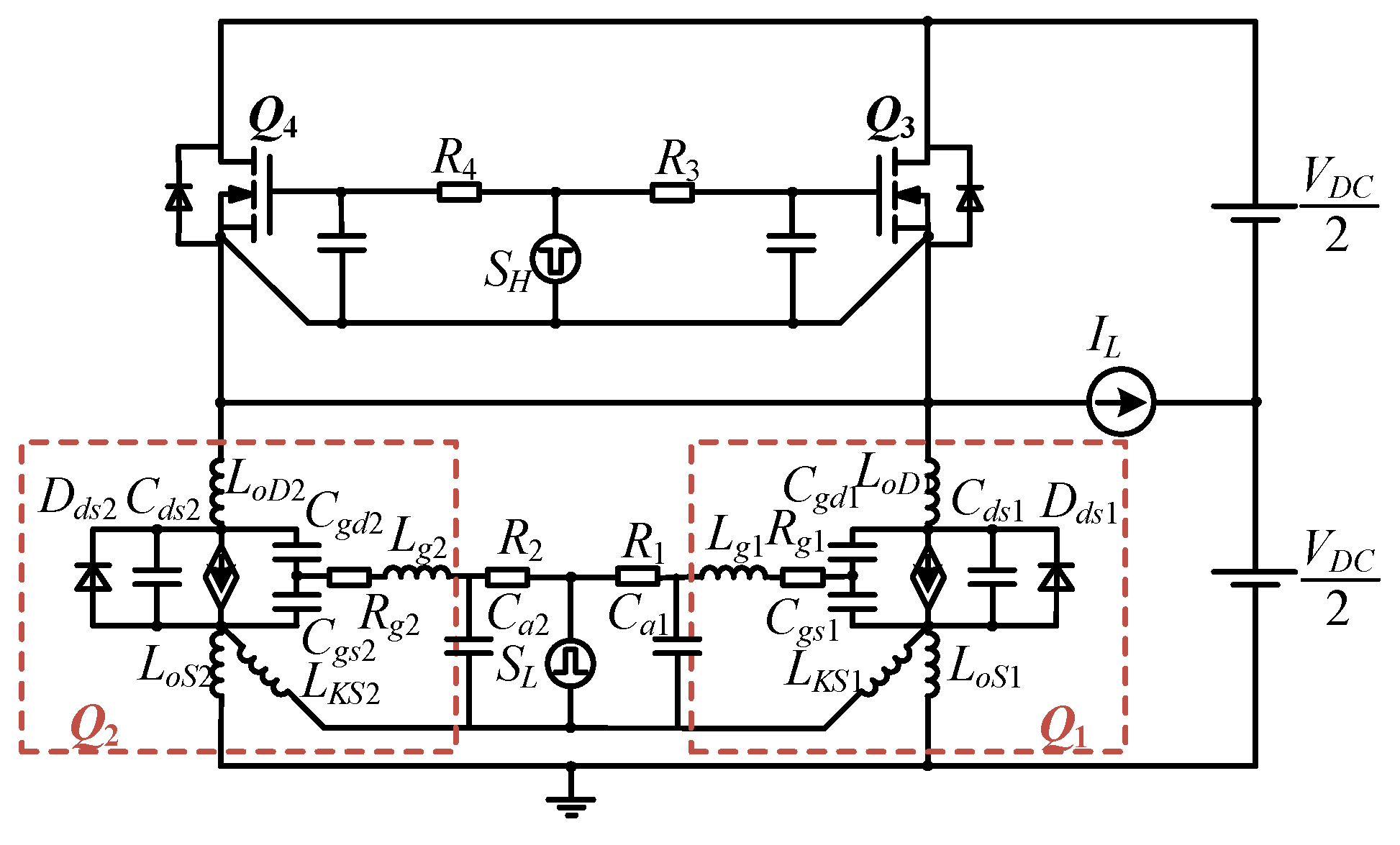
2. Dynamic Model of the Interference Path

To clarify the crosstalk parasitic oscillation mechanism under the conventional gate drive (CGD), this section establishes the power loop and drive loop transfer functions for paralleled SiC MOSFETs in a phase-leg circuit, We further propose a dynamic model to characterize gate voltage disturbances, revealing the interference mechanism of crosstalk-induced parasitic oscillations in parallel SiC MOSFET application.

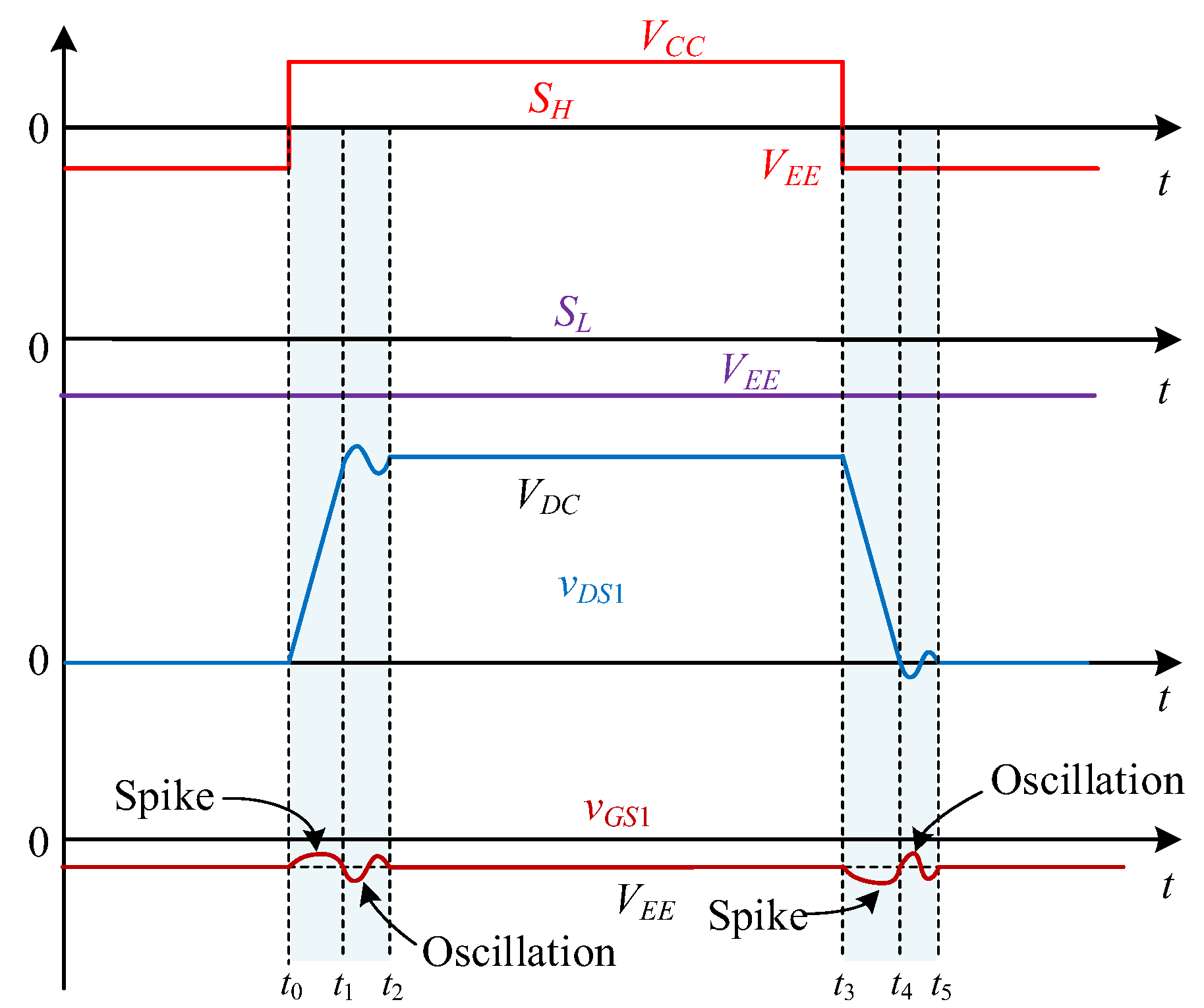
2.1. Typical Voltage Oscillation Phenomenon

Figure 1 depicts the equivalent circuit of a phase-leg configuration with paralleled devices under conventional gate drive (CGD), where drive resistors R1 ~ R4 are explicitly labeled. The drive signals of the gate drive are denoted as SH and SL on the high and low sides, respectively. These circuits are used to analyze the gate voltage performance during the transient process, which is disturbed by the switching action of the active devices Q3 and Q4 on the high side. As an example for analysis, the paralleled devices on the low side are the passive devices, denoted as Q1 and Q2, which are replaced by junction capacitance equivalent circuits for better understanding. If the high-side phase-leg devices Q3 and Q4 are the passive devices, the operation manner is the same because of symmetry. We will not show this in detail because of the limited space. It should be noted that the model’s accuracy depends on the junction capacitance accuracy of the SiC MOSFET, which the power device manufacturers provide inside the datasheet. Most manufacturers would select junction capacitance under the JESD24 standard [37]. The JESD24 standard outlines terms, definitions and procedures for testing power MOSFETs, including electrical verification and thermal characterization. It establishes frameworks for consistent measurement practices, e.g., defining input capacitance, output capacitance and reverse transfer capacitance. Hence, researchers usually believe that the junction capacitance model and the model derived from it are meaningful and appropriate for scientific soundness and knowledge advancement.
The high-side phase-leg devices Q3 and Q4 are connected in parallel. They are treated as the interference source due to the switching actions. In general, SiC MOSFETs operate with significantly higher dv/dt compared to their Si IGBT counterparts. The pulse voltage at the drain-source terminals of active devices is considered the main interference source for the gate voltage of passive devices. For simplification, this paper refers to Q3 and Q4 as the active devices, and to Q1 and Q2 as the passive devices. The dynamic process of load current IL flowing out of the phase-leg is analyzed for simplicity. Because the switching speed is fast and the absolute time of the dynamic process is short, the load current value of the phase-leg structure can be approximated as constant. The load current IL flows in the positive direction from the phase-leg midpoint to the DC bus midpoint is chosen as an example to demonstrate how the current flows into an actual load (resistive and/or capacitive) and works to generate the voltage oscillation phenomenon.
Figure 1 details the phase-leg equivalent circuit with paralleled devices under conventional gate drive (CGD). In Figure 1, the junction capacitance equivalent circuits are denoted as follows. This paper considers the widely used discrete Kelvin package, such as TO247-4. The four pins of the device are denoted as gate (G), drain (D), Kelvin source (KS), and power source (S), respectively. The corresponding stray inductances of the pins are Lg, Ld, Lks, and Ls, respectively. The internal gate resistance of the SiC MOSFET is denoted as Rg. As usual, Cgs, Cgd, and Cds represent the internal junction capacitances, where Ciss = Cgs + Cgd, Coss = Cgd + Cds, and Crss = Cgd. The channel current of the SiC MOSFET is denoted as id, and the parasitic body diode as Dds. The corner marks 1 and 2 are denoted to separate each device.
Figure 2 demonstrates the crosstalk-induced parasitic oscillation phenomenon in the SiC MOSFET parallel phase-leg configuration shown in Figure 1. In Figure 2, vGS1 represents the gate voltage of Q1, while vDS1 denotes its drain-source voltage. SH is the drive signal of the active devices Q3 and Q4, and SL is the drive signal of the passive devices Q1 and Q2. The drive signal SL of the passive devices Q1 and Q2 remains at the turn-off bias level VEE to illustrate the interference path during the double-pulse test, which is also a simplification for the interference path during the dead time of the phase-leg configuration in a converter.
At time t0, the drive signal SH of the active devices Q3 and Q4 starts to rise to the turn-on bias level VCC, and the active devices Q3 and Q4 gradually turn on, causing the drain-source voltage vDS1 of the passive device Q1 to start rising. This results in interference with the gate voltage vGS1 of the passive device Q1, and the detailed mechanism proceeds as follows:
Stage 1 [t0, t1]: At the time-instance t0, the drive signal SH transitions from VEE to VCC, and QH (refers to Q3 and Q4) turns on, causing the drain voltage of high-side devices vDS3 to drop to nearly 0 V. Meanwhile, the drive signal of the low-side devices SL remains at a low level; the QL (refers to Q1 and Q2) channel remains off while its parasitic diodes act as freewheeling diodes. According to KVL, VDC = vDS3 + vDS1, so the vDS1 (drain voltage of Q1) gradually increases from 0 to VDC. During this stage, the rise in vDS1 also causes the gate-drain parasitic capacitance Cgd1 to generate a displacement current igd1, which flows into the drive circuit of Q1, leading to a forward voltage spike in the gate voltage of Q1. This mode ends when vDS1 reaches VDC for the first time.
Stage 2 [t1, t2]: At the time-instance t1, the Q1 drain voltage vDS1 rises to VDC. At this stage, the high-frequency oscillation of vDS1 will excite the Q1 gate voltage vGS1 to generate a high-frequency crosstalk parasitic oscillation, and the oscillation lasts until the moment of t2, when the Q1 gate voltage vGS1 returns to the negative turn-off bias voltage VEE. Thus, it enters a new steady state.
Stage 3 [t2, t3]: The gate voltage of the high-side device is maintained at the positive conduction bias voltage VCC, the channel of Q1 has a continued flow of load current, and the gate voltage of Q1 is maintained at the negative turn-off bias voltage VEE.
Stage 4 [t3, t4]: During this stage, the gate voltage vGS1 perturbation is caused by the decrease in the drain voltage vDS1 and further decreases to generate a negative voltage spike. This mode ends at the time-instance t4 when the drain voltage vDS1 decreases to 0.
Stage 5 [t4, t5]: At the time-instance t4, the drain voltage vDS1 goes back to near the bias voltage VEE. During this stage, the high-frequency oscillation of vDS1 will excite the Q1 gate voltage vGS1 to generate high-frequency crosstalk parasitic oscillation, and the oscillation continues until the moment of t5, when the Q1 gate voltage vGS1 returns to the turn-off bias voltage VEE, and enters a new steady-state process.
After time-instance t5, the waveforms would show cyclic repetition, starting again from t0. In addition, as it is symmetric, the interference crosstalk parasitic oscillation of Q2 is similar to that of Q1. It will not be further described from stage to stage due to space limitations.
From the preceding analysis, crosstalk parasitic oscillation occurs during switching dynamic processes, primarily triggered by variations in the drain voltage vDS1. Owing to their inherently higher dv/dt capability compared to Si IGBT, SiC MOSFETs exhibit pulsed drain-source voltages that act as the dominant interference source for passive devices’ gate voltages. Specifically, the pulsed drain voltage of SiC MOSFETs is the primary interference source of the voltage oscillation at the passive device’s gate, which contains abundant harmonics in high-frequency bands during high-speed switching. These dynamics are categorized into two phases: The first phase involves a typical interference-induced gate voltage spike, occurring during [t0, t1] and [t3, t4]. The second phase consists of high-frequency crosstalk parasitic oscillations, occurring during [t1, t2] and [t4, t5].
To address high-frequency oscillations above the switching frequency, this paper develops a dynamic model to analyze crosstalk parasitic oscillations originating from the active device switching. This model enables the prediction and calculation of the dynamic component of the gate voltage response to the disturbance of the pulsed and oscillating drain voltage.
The dynamic model is a double-input, double-output system. The double inputs are the disturbance voltage source and the drive signal; the double outputs are the gate voltages of the parallel devices. For a better understanding, this dynamic model is described with the disturbance component and the drive component.

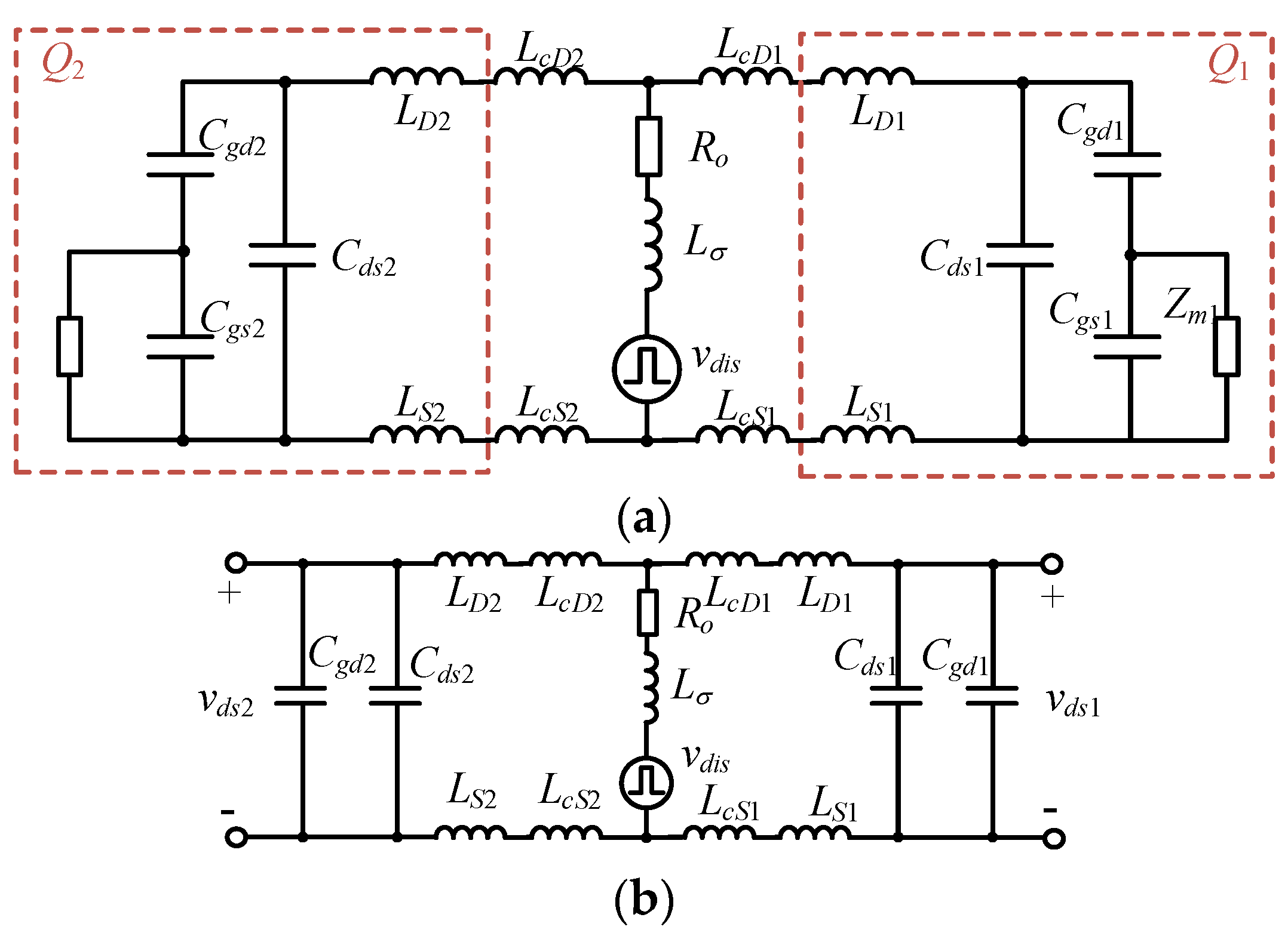
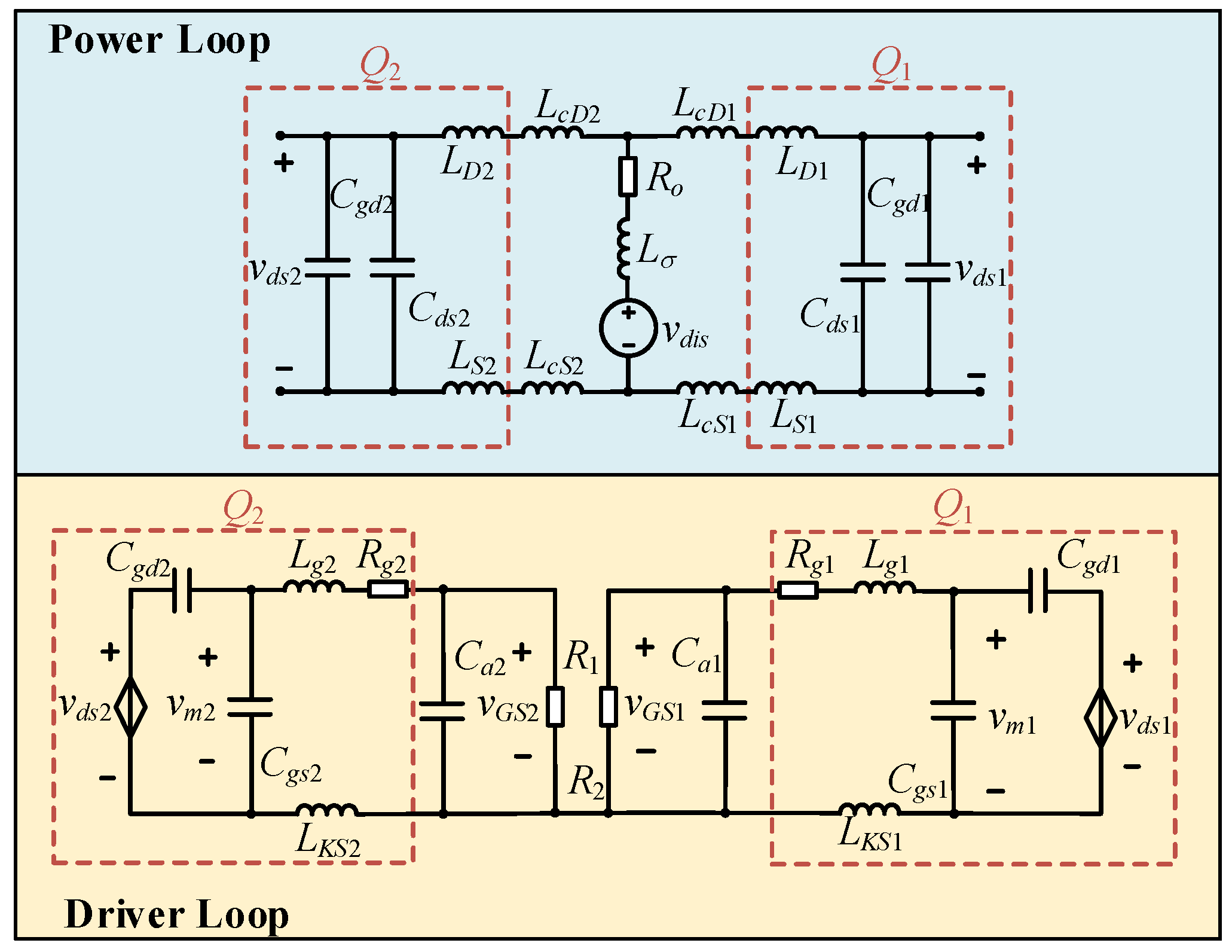
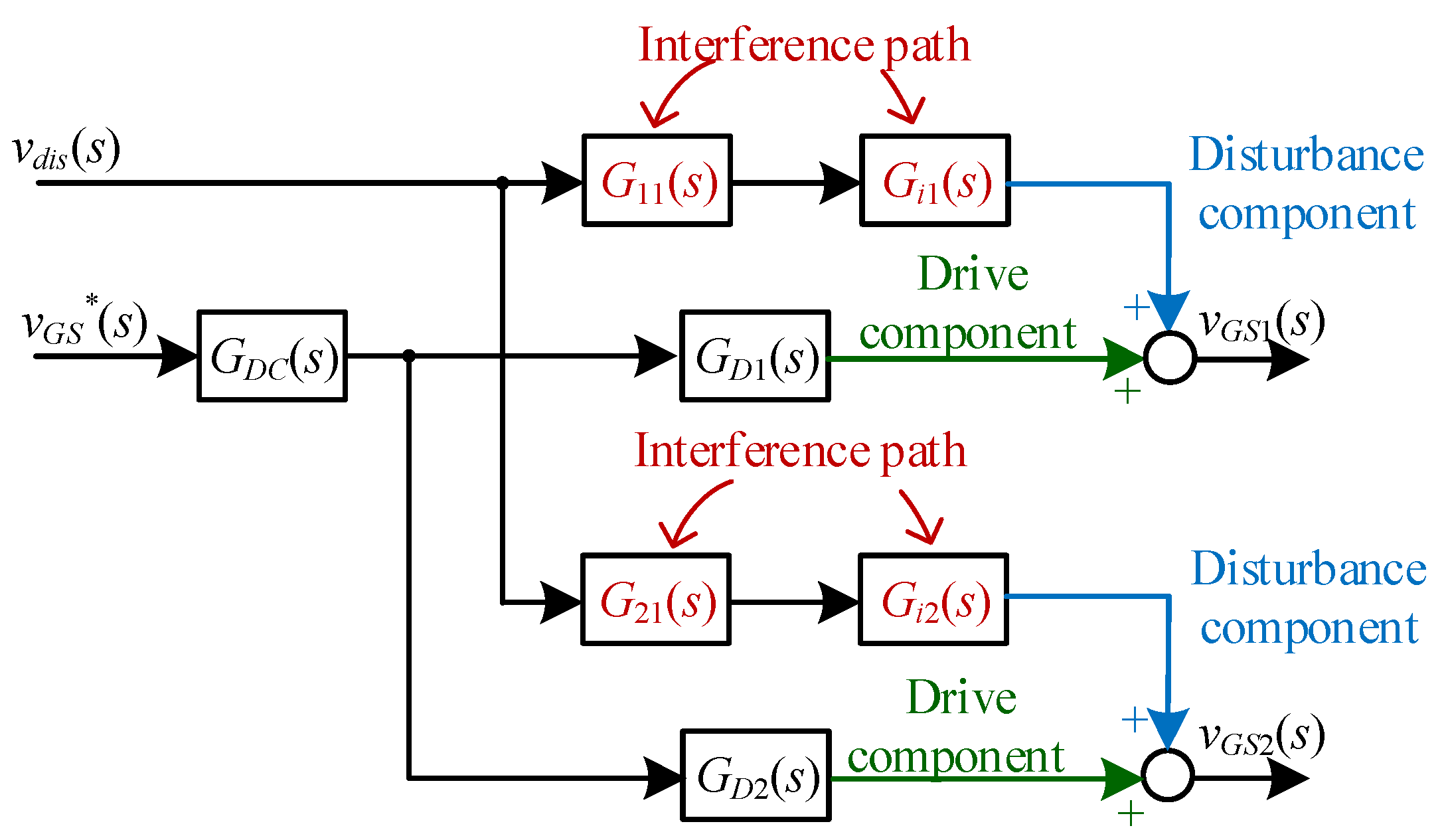
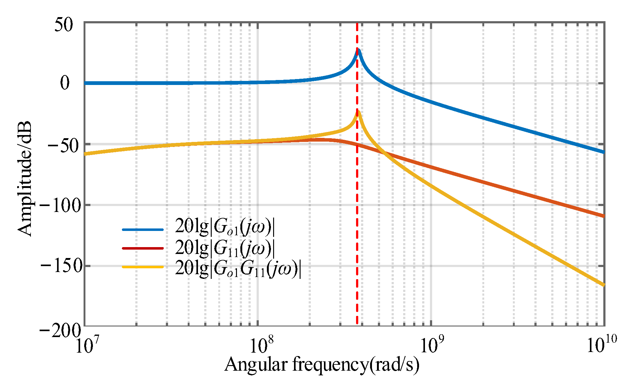
2.2. Dynamic Model: Disturbance Component

To derive the disturbance component of the dynamic model, i.e., coupling from the disturbance voltage source vdis to gate voltages, according to the superposition principle, the drive signal vGS* is set to zero at first. Subsequently, Figure 1 is further simplified to obtain the equivalent circuit in Figure 3, isolating the path from the disturbance voltage source vdis to the gate voltages.
In Figure 3, vdis represents the pulsed drain voltage, which is treated as the disturbance voltage source. The power loop inductance Lσ encompasses active device lead inductance and stray inductance (between the DC capacitor and phase-leg circuit). Ro denotes the total equivalent resistance in the power loop, including PCB trace resistance and the MOSFETs’ on-resistance. LcD1 and LcD2 are drain-side power line inductances, while LcS1 and LcS2 represent source-side inductances of passive devices. LD1 and LD2 represent the drain pin inductances, and LS1 and LS2 represent the power source pin inductances of the passive devices. For linearization, this paper assumes Cgs, Cgd and Cds as constants and neglects parasitic body diode reverse recovery effects.
As shown in Figure 3a, the voltage across Cds1 is vds1, the voltage across Cds2 is vds2, the voltage at the midpoint between Cgd1 and Cgs1 is vm1 and the voltage between Cgd2 and Cgs2 is vm2. In numerical terms, the voltages vm1 and vm2 in the drive loop are much smaller than those of the power loop vds1 and vds2. Therefore, to demonstrate the behavior of the power loop, vm1 and vm2 are treated as 0 for simplification. Thus, the part from vdis to vds1 and vds2 can be approximated to be independent of Zm1 and Zm2 (the drive loop impedances of two parallel devices). Finally, the simplified equivalent circuit in Figure 3b is derived.
In Figure 3b, the drive loop is decoupled from the power loop, where Cgd1, Cds1 and Cgd2, Cds2 are directly paralleled. The transfer functions from the disturbance voltage source vdis to the drain-source capacitance voltages vds1 and vds2 are as follows:
G 11 ( s ) = v d s 1 v d i s = 1 [ L σ ( C o s s 1 + C o s s 2 ) + 2 C o s s 1 ( L o d 1 + L o s 1 ) + C o s s 2 ( L o d 2 + L o s 2 ) ] s 2 + R o ( C o s s 1 + C o s s 2 ) s + 1
G 21 ( s ) = v d s 2 v d i s = 1 [ L σ ( C o s s 1 + C o s s 2 ) + C o s s 1 ( L o d 1 + L o s 1 ) + 2 C o s s 2 ( L o d 2 + L o s 2 ) ] s 2 + R o ( C o s s 1 + C o s s 2 ) s + 1
where Lod1 and Lod2 represent the drain power line inductance of the passive devices, including their pin inductances, e.g., Lod1 = LcD1 + LD1, Lod2 = LcD2 + LD2; similarly, Los1 and Los2 represent the power line inductance at the power source terminals of the passive devices, including their pin inductances, e.g., Los1 = LcS1 + LS1, Los2 = LcS2 + LS2.
Furthermore, the transfer functions from drain-source capacitance voltages vds1 and vds2 to vm1 and vm2 can be derived as follows:
G 12 ( s ) = v m 1 v d s 1 = Z m 1 | | 1 C g s 1 s 1 C g d 1 s + Z m 1 | | 1 C g s 1 s
G 22 ( s ) = v m 2 v d s 2 = Z m 2 | | 1 C g s 2 s 1 C g d 2 s + Z m 2 | | 1 C g s 2 s
where Zm1 = Rg1 + s(Lg1 + LKS1) + R1 || (1/sCa1) and Zm2 = Rg2 + s(Lg2 + LKS2) + R2 || (1/sCa2). Among them, Ca1 and Ca2 are the potential auxiliary capacitors. Rg1 and Rg2 represent the gate internal resistances, and R1 and R2 represent the driving resistances of the parallel-connected passive devices. Lg1 and Lg2 represent the gate line inductances and pin inductances, while LKS1 and LKS2 represent the Kelvin source line inductances and pin inductances of the parallel-connected passive devices, respectively.
To calculate the gate voltage vGS1 and vGS2 of the disturbed parallel devices obtained (at both ends of the pins), taking their respective external parallel impedances of the gates Z1 = R1 || (1/sCa1) and Z2 = R2 || (1/sCa2), we have
G 13 ( s ) = v G S 1 v m 1 = Z 1 Z m 1 = Z 1 R g 1 + s ( L g 1 + L K S 1 ) + Z 1
G 23 ( s ) = v G S 2 v m 2 = Z 2 Z m 2 = Z 2 R g 2 + s ( L g 2 + L K S 2 ) + Z 2
Based on Equations (1) to (6), the transfer functions of the crosstalk parasitic oscillation of each parallel device based on the power loop are derived:
G 11 ( s ) = 1 [ L σ ( C o s s 1 + C o s s 2 ) + 2 C o s s 1 ( L o d 1 + L o s 1 ) + C o s s 2 ( L o d 2 + L o s 2 ) ] s 2 + R o ( C o s s 1 + C o s s 2 ) s + 1 G i 1 ( s ) = G 12 ( s ) G 13 ( s ) = R 1 C g d 1 ( R 1 + R g 1 ) s [ R 1 C a 1 L i 1 + 2 C i s s 1 ( L i 1 + R 1 R g 1 C a 1 ) ( R 1 + R g 1 ) + R 1 C a 1 ( L i 1 + R 1 R g 1 C a 1 ) ] s 2 + [ L i 1 + R 1 R g 1 C a 1 + C i s s 1 ( R 1 + R g 1 ) 2 + R 1 C a 1 ( R 1 + R g 1 ) ] s + ( R 1 + R g 1 ) v G S 1 ( s ) v d i s ( s ) = G 11 ( s ) G i 1 ( s )
G 21 ( s ) = 1 [ L σ ( C o s s 1 + C o s s 2 ) + C o s s 1 ( L o d 1 + L o s 1 ) + 2 C o s s 2 ( L o d 2 + L o s 2 ) ] s 2 + R o ( C o s s 1 + C o s s 2 ) s + 1 G i 2 ( s ) = G 22 ( s ) G 23 ( s ) = R 2 C g d 2 ( R 2 + R g 2 ) s [ R 2 C a 2 L i 2 + 2 C i s s 2 ( L i 2 + R 2 R g 2 C a 2 ) ( R 2 + R g 2 ) + R 2 C a 2 ( L i 2 + R 2 R g 2 C a 2 ) ] s 2 + [ L i 2 + R 2 R g 2 C a 2 + C i s s 2 ( R 2 + R g 2 ) 2 + R 2 C a 2 ( R 2 + R g 2 ) ] s + ( R 2 + R g 2 ) v G S 2 ( s ) v d i s ( s ) = G o 2 ( s ) G 21 ( s )
where Li1 and Li2 are the sum of the gate line inductance and pin inductance, and the Kelvin source line inductance and pin inductance of the parallel devices, e.g., Li1 = Lg1 + LKS1 and Li2 = Lg2 + LKS2.
Building on this analysis, we derive transfer functions relating the disturbance voltage source vdis to the gate voltages vGS1 and vGS2. For clarity, Equations (7) and (8) are graphically presented in Figure 4, highlighting the interference propagation path. For a specific SiC MOSFET, the time-domain gate voltage response to high-frequency oscillation can be predicted using transient parameters from datasheets. Furthermore, frequency-domain analysis enables the prediction of oscillating characteristics in parallel device applications.

2.3. Dynamic Model: Drive Component

In practical parallel-device applications, the gate voltage is not confined to turned-off bias but incorporates the pulse drive component. Therefore, we extend the disturbance component analysis to derive a comprehensive gate voltage expression accounting for dynamic disturbance effects.
To derive the drive component of the dynamic model, i.e., coupling from drive signal vGS* to gate voltages, we apply the superposition principle by setting the disturbance voltage source vdis to zero.
The drive signal vGS* charges and discharges the gate voltage auxiliary capacitors Ca1, Ca2 and the input capacitors Ciss1, Ciss2 through the drive resistors R1 and R2 of the parallel devices, as shown in Figure 5.
In this context, the transfer function GDC(s) relating the drive signal to the common terminal of the parallel devices can be expressed as
G D C ( s ) = v c v G S * = ( R 2 C i 2 + R g 2 C i s s 2 + R 1 C i 1 + R g 1 C i s s 1 ) s + 1 [ C i L c + R 2 R g 2 C a 2 C i s s 2 + L c g 2 C i 2 + C i s s 2 L i 2 + ( R 1 C i 1 + R g 1 C i s s 1 ) ( R 2 C i 2 + R g 2 C i s s 2 ) + R 1 R g 1 C a 1 C i s s 1 + L c g 1 C i 1 + C i s s 1 L i 1 ] s 2 + ( R 2 C i 2 + R g 2 C i s s 2 + R 1 C i 1 + R g 1 C i s s 1 ) s + 1
Furthermore, based on the impedance relationships in the equivalent circuit shown in Figure 5, the transfer functions GD1(s) and GD2(s) from vc (the drive voltage at the common terminal of the parallel devices) to vGS1 and vGS2 can be obtained:
G D 1 ( s ) = v G S 1 v c = R g 1 C i s s 1 s + 1 ( R 1 R g 1 C a 1 C i s s 1 + L c g 1 C i 1 + C i s s 1 L i 1 ) s 2 + ( R 1 C i 1 + R g 1 C i s s 1 ) s + 1
G D 2 ( s ) = v G S 2 v c = R g 2 C i s s 2 s + 1 ( R 2 R g 2 C a 2 C i s s 2 + L c g 2 C i 2 + C i s s 2 L i 2 ) s 2 + ( R 2 C i 2 + R g 2 C i s s 2 ) s + 1
Finally, the complete expressions for the gate voltages, including the disturbance component and the drive component, can be obtained according to the superposition principle:
v G S 1 ( s ) = [ G o 1 ( s ) G i 1 ( s ) G D C ( s ) G D 1 ( s ) ] [ v d i s ( s ) v G S * ] v G S 2 ( s ) = [ G o 2 ( s ) G i 2 ( s ) G D C ( s ) G D 2 ( s ) ] [ v d i s ( s ) v G S * ]
Figure 6 presents the block diagram corresponding to Equation (12), illustrating both interference propagation paths and complete gate voltage expressions. Here, the disturbance component refers to the portion of the gate voltage vGS perturbed by the disturbance source via interference coupling. Conversely, the drive component describes the ideal charging and discharging process of the drive signal vGS* through the drive resistor to the respective gate voltage in the ideal case, without disturbance effects. The complete gate voltage expressions are obtained by summing the disturbance and drive components for each device.
The dynamic model makes it possible to mathematically analyze the crosstalk parasitic oscillation operation principle and propose a suppression strategy with precise feedback control.

3. Crosstalk Parasitic Oscillation Suppression Strategy

In industrial applications, SiC MOSFETs are frequently paralleled to enhance converter power capability through current handling capacity scaling. However, the gate voltage interference path in parallel configurations exhibits significantly higher complexity compared to single-device operation. Leveraging the proposed dynamic model, the frequency-domain analysis is necessary for a better understanding, providing the oscillation suppression strategy with the novel insight provided by the dynamic model.

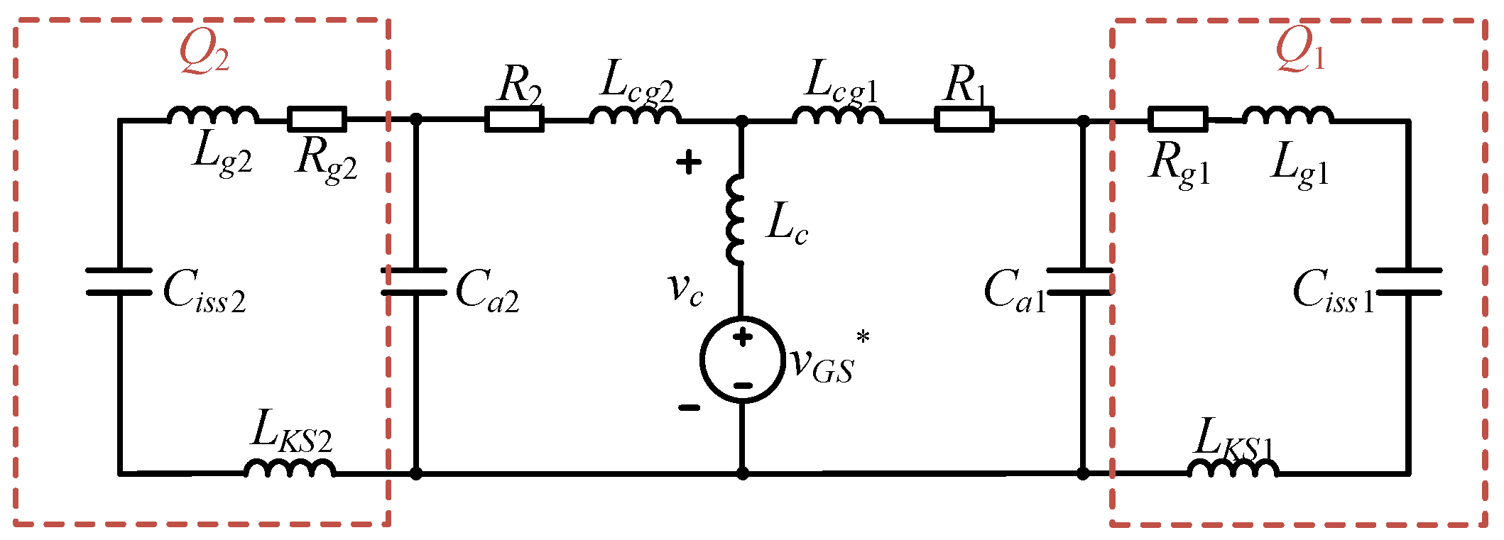
3.1. Crosstalk Parasitic Oscillation in Parallel Devices

From Equation (7), the power loop transfer functions G11(s) and G21(s) and the parallel devices’ interference paths have standard second-order system characteristics. From the transfer functions, it is easy to obtain the parallel devices’ power loop natural undamped frequency as
ω n o 1 = 1 L σ ( C o s s 1 + C o s s 2 ) + 2 C o s s 1 ( L o d 1 + L o s 1 ) + C o s s 2 ( L o d 2 + L o s 2 )
The parallel devices’ power loop damping ratio is
ζ o 1 = R o ( C o s s 1 + C o s s 2 ) 2 L σ ( C o s s 1 + C o s s 2 ) + 2 C o s s 1 ( L o d 1 + L o s 1 ) + C o s s 2 ( L o d 2 + L o s 2 )
The parameters of a typical industrial 1200 V 45 mΩ SiC MOSFET used as an example for analysis with the dynamic model are shown in Table 2, which are the parameters of IMZ120R045M1.
Taking the drive resistor R1 = 10 Ω, R2 = 10 Ω and gate terminals auxiliary shunt capacitance Ca1 = 1 nF, Ca2 = 1 nF, it is estimated that the power loop inductance is Lσ = 20 nH, the power loop stray resistance (including the devices’ on-resistance and the line resistance) is about Ro = 0.5 Ω, and the device pin inductance is about 10 nH. From Equation (7), the transfer function amplitude of the gate voltage disturbance for one of the parallel devices can be obtained, as shown in Figure 7. It should be noted that this figure is a Bode plot; hence, the horizontal axis uses the angular frequency (rad/s) instead of the frequency (Hz).

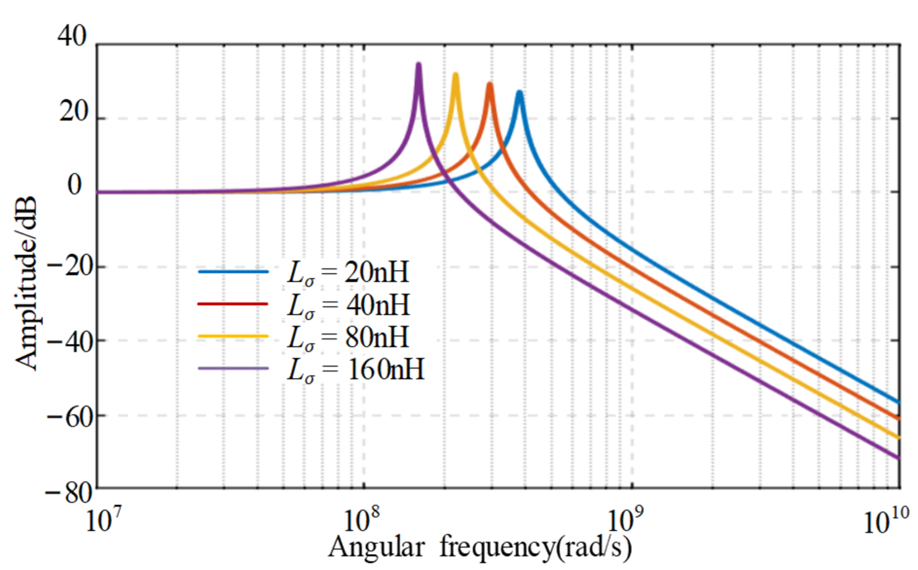
3.1.1. Impact of Power Loop Stray Inductance

As Figure 7 demonstrates, the power loop transfer function exhibits a pronounced resonance peak at 60.68 MHz with a magnitude of 27.1282 dB. This resonance is coupled to the gate voltage via the driver loop, owing to the drive loop transfer function’s insufficient high-frequency attenuation. Consequently, high-amplitude oscillations emerge at the passive device’s gate voltage.
From Equations (13) and (14), it can be observed that the size of the power stray inductance affects both the natural undamped frequency and the damping ratio of the power loop transfer function G11(s) of the parallel devices. Taking the parallel device in Table 1 as an example, the transfer function G11(s) amplitude of the gate voltage interference path under different power stray inductances can be plotted according to Equation (7), as shown in Figure 8.
As Figure 8 reveals, increasing Lσ from 20 nH to 160 nH, its undamped natural frequency decreases from 60.723 MHz to 25.48 MHz, a decrease of 58.03%, and the resonance peak increases from 27.1105 to 34.7, an increase of 27.3%. It should also be noted that the 160 nH stray inductance is very large and not ordinary in application. However, this paper only uses this value to demonstrate that the resonant frequency will gradually decrease with the increase in stray inductance.
An increase in power loop stray inductance Lσ lowers the natural frequency and damping ratio of the power loop, thereby degrading oscillation suppression capability. With a reduced damping ratio, the relative resonance peak Mro amplifies, collectively exacerbating the amplitude of high-frequency oscillations coupled to the gate voltage.
Thus, in SiC MOSFET applications, minimizing Lσ through optimized PCB design and packaging techniques is critical for mitigating crosstalk-induced parasitic oscillations and enhancing system reliability.
The resonant frequency ωro1 and the relative resonant peak Mro1 of the power loop transfer function Go1(s) can be obtained from the damped self-oscillating frequency and damping ratio:
ω r o 1 = ω n o 1 1 2 ζ o 1 2 M r o 1 = 1 2 ζ o 1 1 ζ o 1 2
According to Equation (15), the high-frequency oscillation frequency of the gate voltage is primarily determined by the power loop inductance Lσ and the two output capacitances Coss1 and Coss2 of the parallel devices. Although the change in drain voltage vds causes a change in the output capacitance during the switching process of the SiC MOSFETs, this change is so small at the moment when high-frequency oscillations occur that it can be ignored. Therefore, typical output capacitance values from the SiC MOSFET datasheet can be used for calculation.
In summary, during high-speed switching, the passive devices experience disturbances from the voltage variation in the active devices. These disturbances propagate via stray inductance, parallel line inductance and the passive device’s junction capacitance, inducing gate voltage perturbations. Furthermore, the system’s stray inductance resonates with the parallel devices’ output capacitance, exciting crosstalk parasitic oscillation.

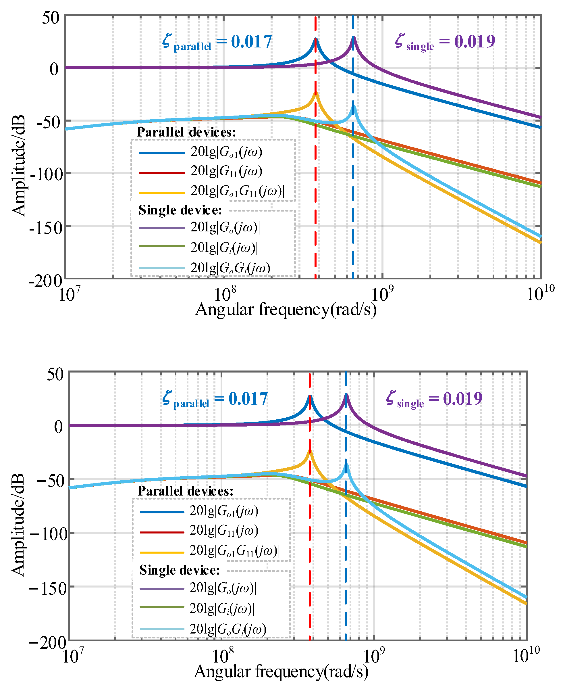
3.1.2. Comparison Between Parallel Devices and Single Device

To better understand the different performance between parallel devices and single devices, we further analyzed the gate voltage interference path between parallel and single devices under the same operation condition. The equivalent circuit diagram of a single SiC MOSFET under high-frequency switching is similar to that of a parallel-connected SiC MOSFET, as shown in Figure 1; only Q1 and Q3 are connected. The derivation of the analytical expression for the gate voltage interference path in the single device is as follows:
G o ( s ) = 1 L σ C o s s s 2 + R o C o s s s + 1 G i ( s ) = R C r s s s R C a L i C i s s s 3 + ( R R g C a C i s s + L i C i s s ) s 2 + ( R g C i s s + R C i s s + R C a ) s + 1 v G S ( s ) v d i s ( s ) = G o ( s ) G i ( s )
where vGS denotes the gate voltage of Q1.
From Equation (16), for a single-device condition, the natural undamped frequency of the power loop transfer function Go(s) of the power loop is
ω n o = 1 L σ C o s s
The power loop damping ratio of the single-device condition is
ζ o = R o 2 C o s s L σ
Using the same parasitic parameters as the parallel configuration, the gate voltage disturbance transfer function amplitude is derived from Equation (16), as shown in Figure 9. In addition, from Equations (14) and (18), and by combining the parameters in Table 1, it can be calculated that, compared with the power loop transfer function Go(s) of a single device, the power loop transfer function G11(s) of the parallel devices has a lower damping ratio. At their respective resonance frequencies, the damping ratio of the transfer function of the parallel devices is 0.017, while that of the single device is 0.019, as shown in Figure 9. This reduced damping ratio is coupled to the gate voltage through the drive loop. Moreover, the parallel devices have a lower resonance frequency of 105.41 MHz, while the resonance frequency of the single device is 60.37 MHz. The cutoff frequency of the power loop transfer function of the parallel devices is also lower. Compared with that of the single device, the cutoff frequency of the parallel devices is reduced by 42.63%, containing a lower oscillation frequency component. Furthermore, compared with the drive loop transfer function Gi(s) of a single device, the drive loop transfer function Gi1(s) of the parallel devices also has a lower damping ratio and less attenuation in the same frequency band.
As analyzed previously, the gate voltage interference path in parallel devices exhibits heightened complexity and sensitivity to parasitic stray parameters. Consequently, crosstalk-induced parasitic oscillations are exacerbated in parallel configurations compared to single-device operation, necessitating dedicated suppression strategies for parallel SiC MOSFET applications.

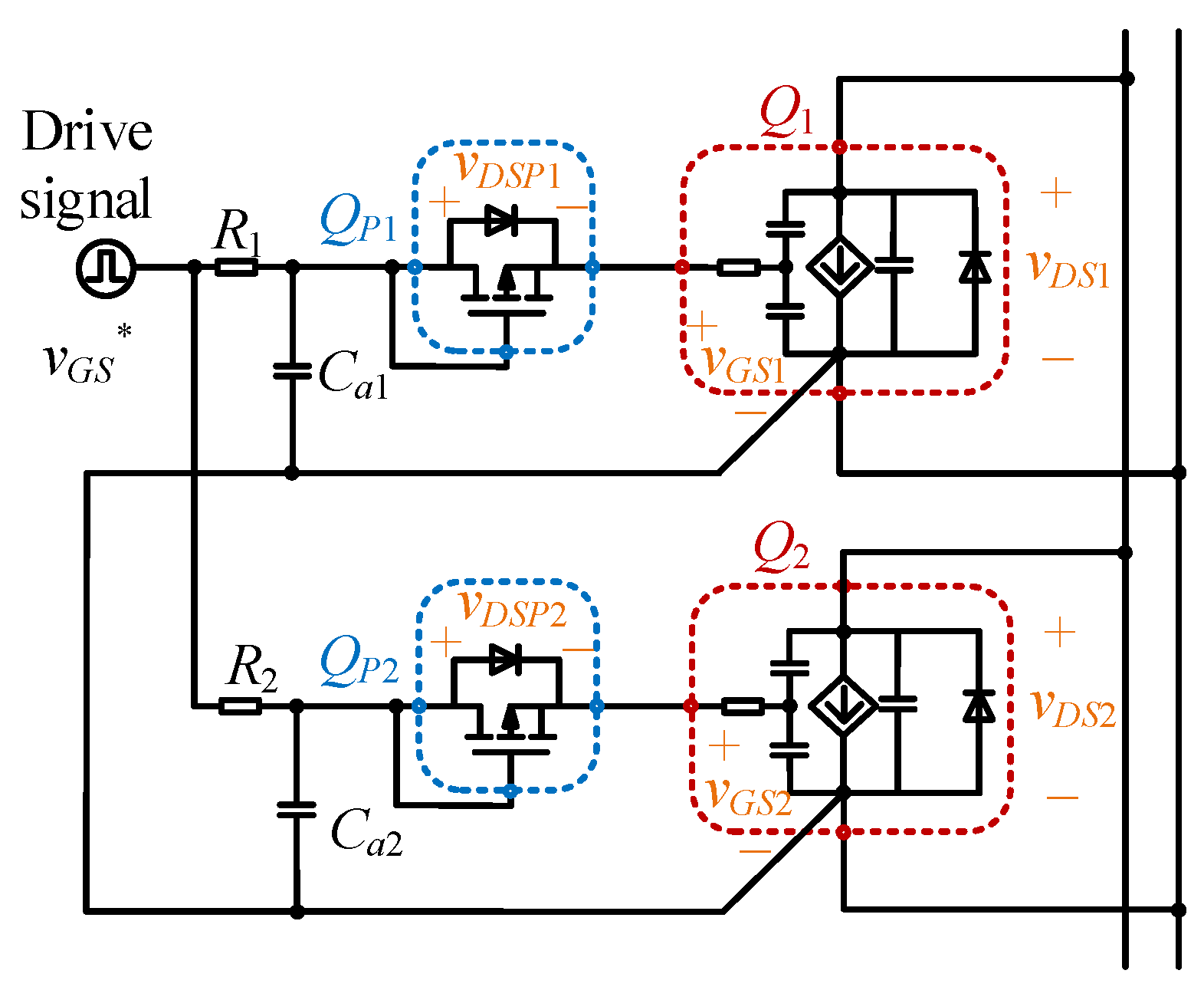
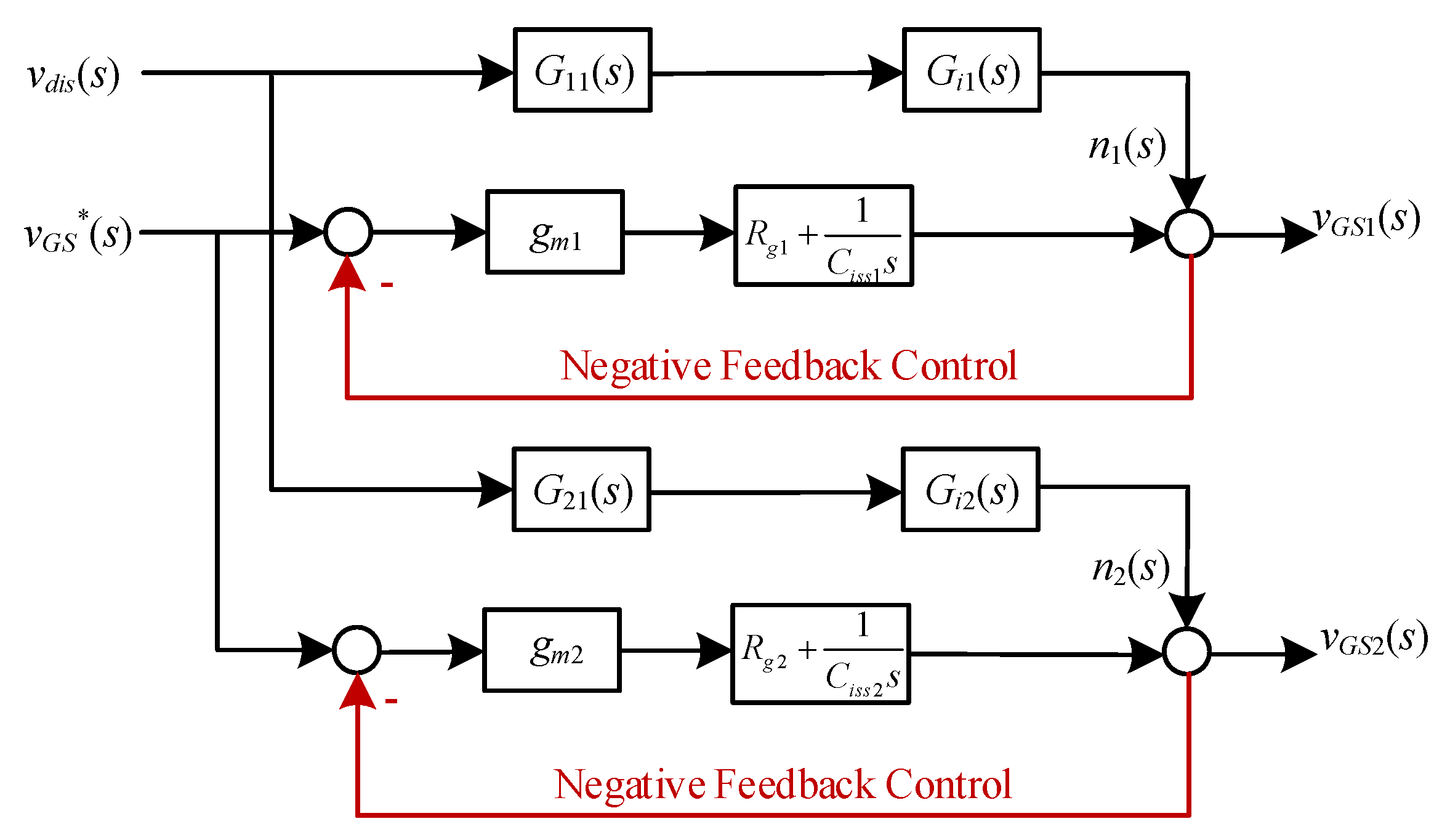
3.2. Operation Principle of NFAGD in Parallel Devices

To mitigate oscillation-induced instability and overstress that degrade device lifetime, the following section presents a suppression strategy leveraging closed-loop feedback control.
Figure 6 shows that the driver circuit is an open-loop system from vGS* to vGS1 and vGS2. When SiC MOSFET devices are applied in parallel, pulse voltage interference can couple to the gate through the parallel line inductance and Miller capacitance, disturbing the gate voltage of the parallel devices. To suppress this disturbance, a feedback closed-loop can be constructed, as shown in Figure 10.
Figure 10 illustrates the crosstalk parasitic oscillation suppression strategy. An ordinary SiC MOSFET driver chip is employed to generate the drive signal vGS*, and P-channel auxiliary MOSFETs QP1 and QP2 are added near the gates of the two paralleled SiC MOSFETs, giving Q1 and Q2 as an example. As this kind of gate driver uses active devices and a negative feedback control method, it is called Negative Feedback Active Gate Drive (NFAGD) for short.
In Figure 10, the drain and gate of the P-channel auxiliary MOSFET are connected together, and the gate-source voltage of the P-channel auxiliary MOSFET is the difference between the drive signal vGS* of the driven SiC MOSFETs and its own gate-source voltage, which is exactly the voltage error signal of the closed-loop control system in Figure 11.
Furthermore, the current flowing through the P-channel auxiliary MOSFET is controlled by its own transconductance gm, depending on its gate-source voltage. Therefore, the circuit in Figure 10 forms the closed-loop control system in Figure 11 by connecting the drain and gate of the two P-channel auxiliary MOSFETs QP1 and QP2, utilizing their respective gains, gm1 and gm2.
Take one of the parallel devices of the two passive devices as an example to explain its operation principle. SiC MOSFET Q1 in Figure 10 is used as a passive device to be clamped at turn-off; it needs to resist external disturbance from the pulsed drain voltage. The output voltage of the gate driver chip is the turn-off bias voltage VEE. Therefore, the drive signal vGS* is equal to VEE. In the steady state, the gate voltage vGS1 of Q1 equals the turn-off bias voltage VEE. However, if vGS1 fluctuates due to disturbance, the negative feedback mechanism is triggered.
If a disturbance causes the gate voltage vGS1 of Q1 to rise such that SP1’s potential exceeds DP1’s by the threshold voltage, the QP1 channel conducts. The driver chip then discharges the input capacitance Ciss1 of Q1 through the QP1 channel, leading to a decrease in vGS1. Conversely, if the disturbance causes vGS1 to decrease, and the potential of DP1 becomes higher than that of SP1, the QP1 parasitic body diode conducts, charging the input capacitance Ciss1 of Q1, causing vGS1 to increase. This negative feedback mechanism ensures that any vGS1 fluctuations are clamped to the drive signal vGS*.
Figure 11 is the corresponding control block diagram version of the proposed gate driver circuit in Figure 10. It shows that the drive signal vGS* is used as a reference signal in the gate negative feedback control loop. The difference between the reference signal and the gate voltages vGS1 and vGS2 of the driven parallel SiC MOSFETs is used to control their input capacitances Ciss1 and Ciss2. This is achieved through the transconductance gm1 and gm2 of the auxiliary P-channel MOSFETs, with the gate internal resistors Rg1 and Rg2 as the controlled objects.
When considering the disturbances n1(s) and n2(s), a current is generated through the Miller capacitor and can be described with the above dynamic model. This current charges and discharges the input capacitance of the driven parallel SiC MOSFETs, thereby interfering with the gate voltage. If vGS1 and vGS2 increase (or decrease), the difference from the reference value vGS* increases. The transconductance of the auxiliary MOSFETs then regulates the input capacitors, discharging (or charging) them, and restoring vGS1 and vGS2 to stability.
The gate driver circuit does not require additional circuit design. It can be accomplished using only a standard SiC MOSFET driver chip, a driver resistor, an auxiliary MOSFET, and an auxiliary capacitor. The negative feedback control aims to ensure that the parallel SiC MOSFETs’ gate voltages precisely track the drive reference vGS* while rejecting pulsed drain voltage disturbances.

3.3. Parameter Design Recommendation

For the convenience of usage, this paper approximates that the transconductance of the auxiliary MOSFETs QP1 and QP2 are non-time-varying constants gm1 and gm2, and the reverse transconductance of the parasitic diodes is also expressed using gm1 and gm2. At the same time, this paper considers that the on-state threshold of the parasitic diodes in the auxiliary MOSFETs equals the channel’s conduction threshold.
From Figure 11, the closed-loop transfer function Negative Feedback Active Gate Drive (NFAGD) application strategy for parallel SiC MOSFETs is
G d 1 ( s ) = v G S 1 ( s ) v G S * ( s ) = G 1 ( s ) 1 + G 1 ( s ) G d 2 ( s ) = v G S 2 ( s ) v G S * ( s ) = G 2 ( s ) 1 + G 2 ( s )
where G1(s) is the open-loop transfer function of the NFAGD of one of the devices in parallel, and G2(s) is the open-loop transfer function of the NFAGD of the other devices in parallel:
G 1 ( s ) = g m 1 ( R g 1 + 1 C i s s 1 s ) = g m 1 R g 1 C i s s 1 s + 1 C i s s 1 s G 2 ( s ) = g m 2 ( R g 2 + 1 C i s s 2 s ) = g m 2 R g 2 C i s s 2 s + 1 C i s s 2 s
According to the open-loop transfer functions G1(s) and G2(s), it can be determined that the NFAGD application strategy for parallel SiC MOSFETs shown in Figure 10 is a type I system. This system has open-loop gains of gm1/Ciss1 and gm2/Ciss2 with open-loop amplification as follows:
K v 1 = lim s 0 G 1 ( s ) s = g m 1 C i s s 1 K v 2 = lim s 0 G 2 ( s ) s = g m 2 C i s s 2
In general, the input capacitance of the driven parallel SiC MOSFETs is about nF level, and the transconductance of the auxiliary MOSFET of P-channel can be selected as >> 1(S) MOSFET, gm1 >> Ciss1, gm2 >> Ciss2, and the open-loop amplification is sufficiently large, so that, when vGS1 and vGS2 track the vGS* of the rising (falling) slope, the difference between them is the deviation of vGS1 and vGS2, which is very small, and does not affect the turn-on and turn-off effects of the driven parallel SiC MOSFETs.
Moreover, the large open-loop amplification ensures a sufficiently large rejection ratio for the disturbance signals, preventing the noise signals n1(s) and n2(s) from disturbing the gate voltages vGS1 and vGS2.
Building on theoretical foundations, the proposed transconductance-based crosstalk-induced parasitic oscillation suppression strategy for parallel SiC MOSFETs neutralizes interference sources via negative feedback control, automatically stabilizing gate voltages.

4. Experiment Verification

This section shows the experimental verification of the proposed NFAGD application strategy for parallel SiC MOSFETs and its comparison with conventional gate drives. The NFAGD circuit used in the experiments is shown in Figure 10. Its counterpart, the conventional gate drive (CGD), as shown in Figure 1, gives two sets of typical industrial gate drive resistance for comparison: CGD Case 1 refers to a 10 Ω gate drive resistance, while CGD Case 2 refers to a 15 Ω gate drive resistance.
The double-pulse test platform and the synchronous buck converter experimental prototype, including its PCB layout, are both considered, as shown in Figure 12. These two kinds of circuits are composed of phase-leg configurations, which are typical for applications and suffer from crosstalk parasitic oscillation.
Table 3 shows the key parameters for the experimental research used in this paper. The turn-on and turn-off bias voltages are set following the datasheet suggestions and engineering experience. NFAGD parameters are tuned following the methodology in reference [35]. Following the test guidance and equipment recommendation in reference [38], the bandwidth and accuracy of the measurement equipment are high enough, where the Cybertek P6501 probe with a 500 MHz bandwidth measures the voltage waveforms, the PEM CWT1 Rogowski current waveform sensor measures the current waveforms and the power analyzer PA5000H measures efficiency.

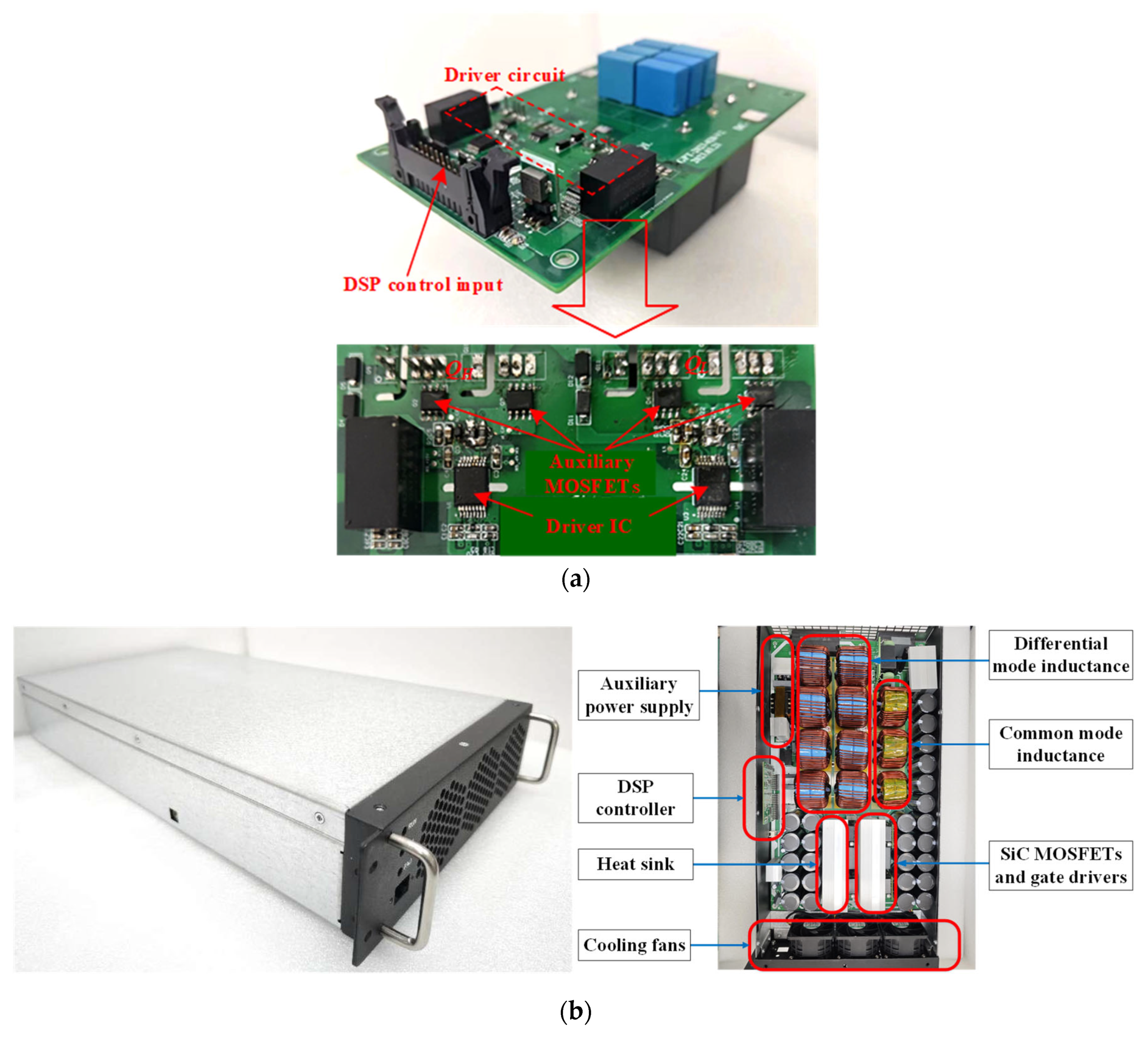
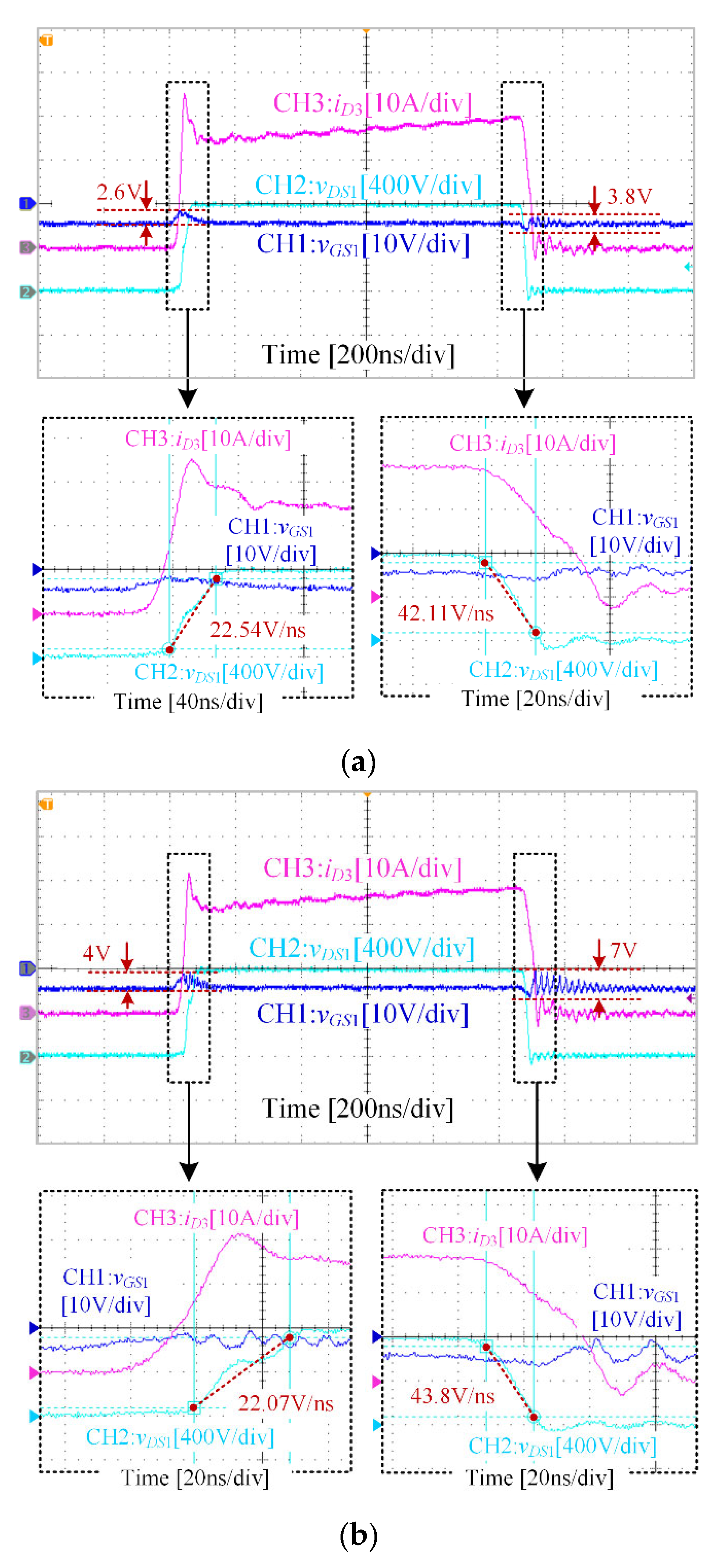
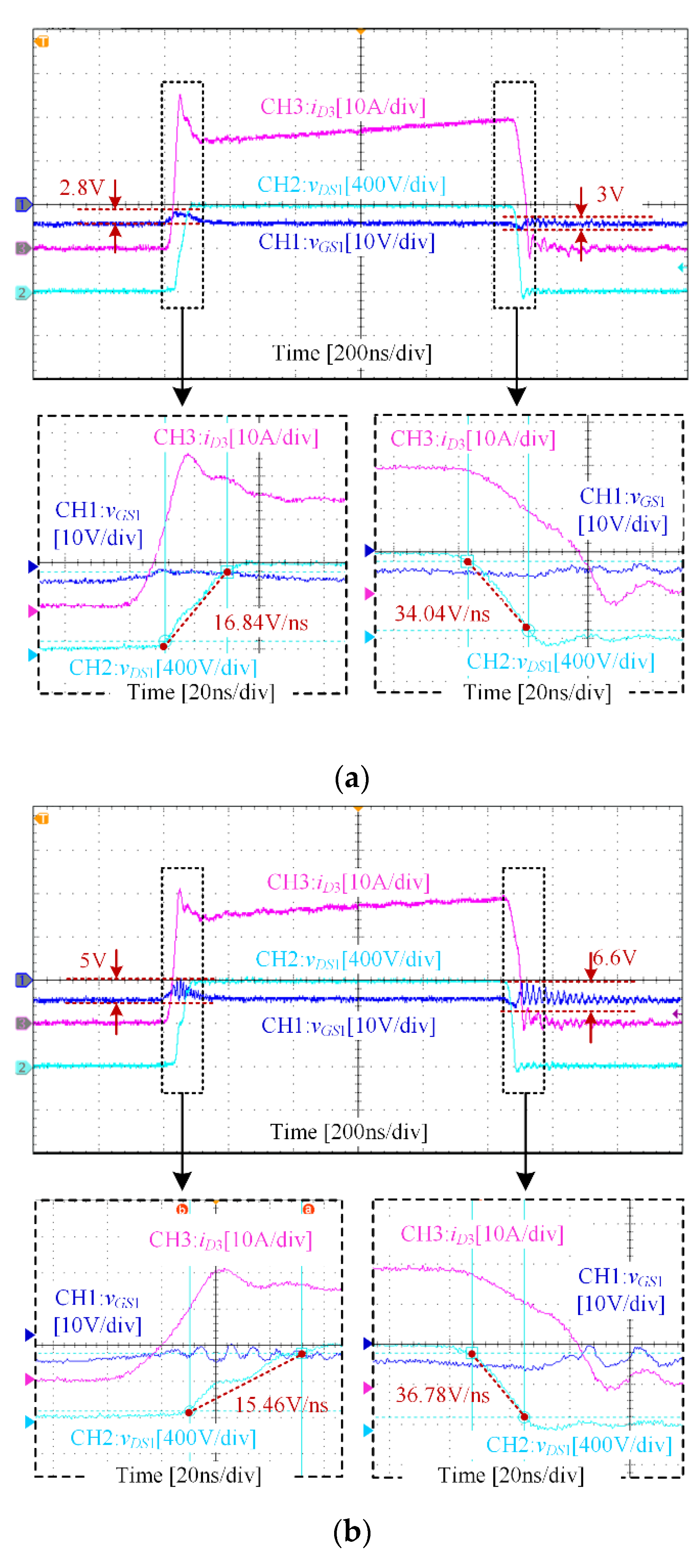
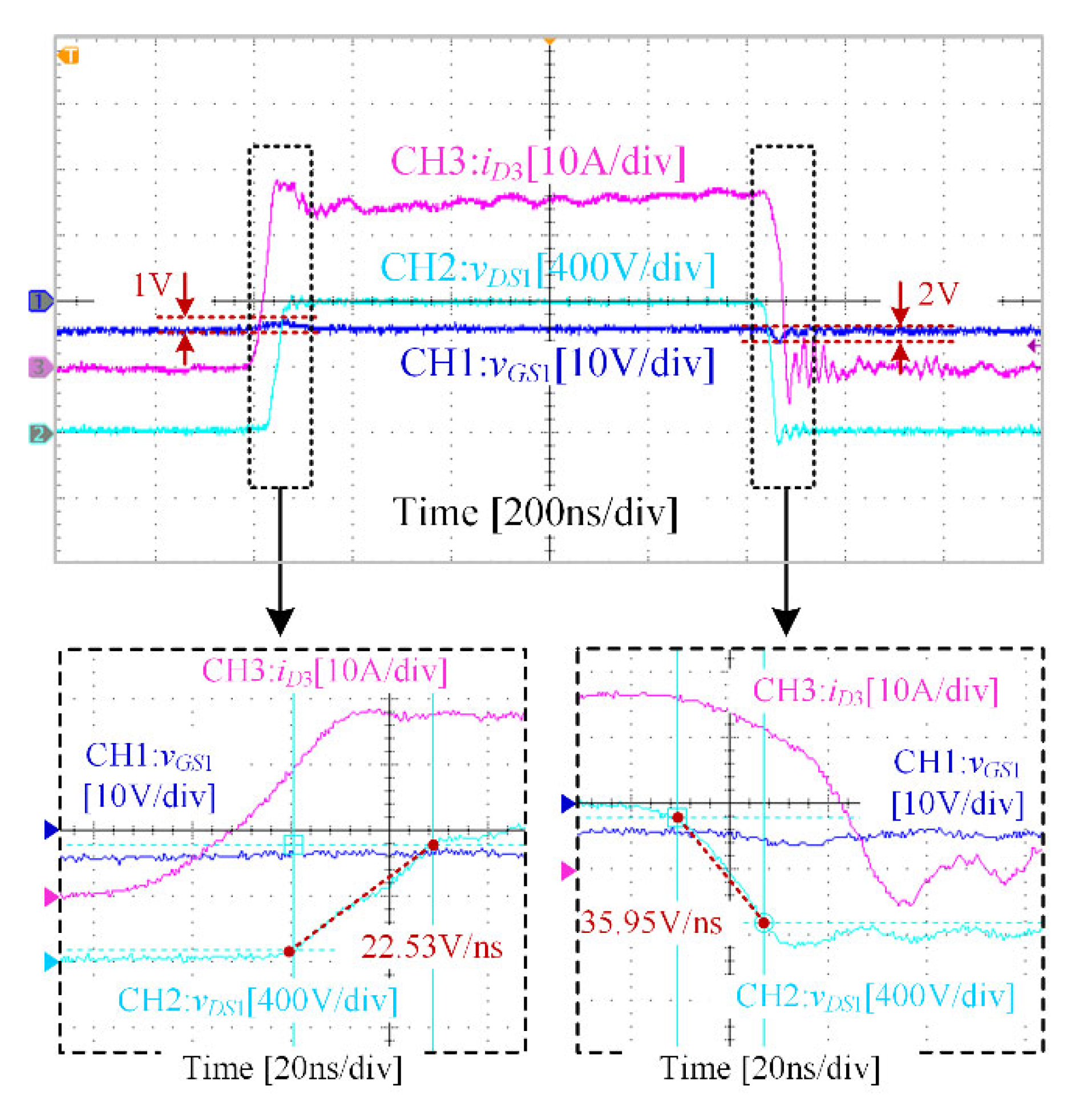
4.1. Double-Pulse Test

The double-pulse test results represent the gate drive performance of gate voltage stability under high dv/dt over 20 V/ns. In this test, the DC input voltage is VDC = 800 V, and the load current is IL = 25 A, as shown in Figure 1.
Figure 13 and Figure 14 show the experimental results of a conventional gate drive (CGD), representing Case 1 and Case 2, respectively. In the double-pulse test, the active device is the high-side one to test the low-side device gate voltages and evaluate the gate drives’ crosstalk parasitic oscillation features. Both the single device and the parallel device conditions are tested. In the parallel devices condition, both the phase-leg Q1 and Q3 and phase-leg Q2 and Q4 are enabled for the double-pulse test. In the single-device condition, only the phase-leg composed of Q1 and Q3 is enabled for the double-pulse test. In the waveforms, CH1 is the gate voltage of Q1, CH2 is the drain voltage of Q1 and CH3 is the drain current of Q3.
Figure 13a demonstrates the waveforms of a single device under CGD Case 1. During the turn-on transient of the active device, the peak-to-peak crosstalk parasitic oscillation is 2.6 V. During the turn-off transient, the peak-to-peak crosstalk parasitic oscillation is 3.8 V. The corresponding dv/dt is 22.54 V/ns and 42.11 V/ns, respectively, which is a very high switching speed of over 20 V/ns. Under this condition, the speed/crosstalk ratio is KSC = 11.08.
For the parallel condition in Figure 13b, the dv/dt during the turn-on transient is 22.07 V/ns, and the dv/dt during the turn-off transient is 43.8 V/ns. The dv/dt during each transient is similar to that of the single-device condition given in Figure 13a. However, the crosstalk parasitic oscillation peak-to-peak voltages are different. During the turn-on transient, the peak-to-peak crosstalk parasitic oscillation is 4 V, 54% higher than the single-device condition, 2.6 V. During the turn-off transient, the peak-to-peak crosstalk parasitic oscillation is 7 V, 84% higher than the single-device condition, 3.8 V. The crosstalk parasitic oscillation in the parallel condition is more severe than in the single-device condition, and the speed/crosstalk ratio decreased to KSC = 6.26, mainly because the gate voltage interference path becomes complex and sensitive to the influence of parasitic stray parameters.
Figure 14a depicts the single-device waveforms under CGD Case 2. During the turn-on transient of the active device, the peak-to-peak crosstalk-induced parasitic oscillation is 2.8 V. During the turn-off transient, the peak-to-peak crosstalk parasitic oscillation is 3 V. The corresponding dv/dt is 16.84 V/ns and 34.04 V/ns, respectively. Neither of the dv/dt is over 20 V/ns. The switching speed is lower than that of CGD Case 1 in Figure 13a. However, the speed/crosstalk ratio is KSC = 11.35, which is kept similar to that in Figure 13a.
For the parallel condition in Figure 14b, the dv/dt during the turn-on transient is 15.46 V/ns, and the dv/dt during the turn-off transient is 36.78 V/ns. The dv/dt during each transient is similar to the single-device condition in Figure 14a. However, the crosstalk parasitic oscillation peak-to-peak voltages are different. During the turn-on transient, the peak-to-peak crosstalk parasitic oscillation is 5 V, 79% higher than the single-device condition. During the turn-off transient, the peak-to-peak crosstalk parasitic oscillation is 6.6 V, 120% higher than the single-device condition. The speed/crosstalk ratio further decreased to KSC = 5.57, indicating that the efficiency would have a high probability of being impacted in the systematic converter application with these gate drive parameters.
Consistent with CGD Case 1, parallel operation in CGD Case 2 exhibits amplified crosstalk-induced parasitic oscillations compared to single-device conditions. Both experimental results cope with the previous analysis given in Equations (7) and (8), where the parallel devices also have a lower damping ratio and less attenuation in the same frequency band; the gate voltage interference path becomes complex and sensitive to the influence of parasitic stray parameters.
The crosstalk parasitic oscillation in CGD Case 2 is suppressed. For the single device, the peak-to-peak crosstalk parasitic oscillation is 3.8 V in Figure 13a under CGD Case 1, while it is 3 V in Figure 14a under CGD Case 2, showing a suppression of approximately 27%. Similarly, for parallel devices, the peak-to-peak crosstalk parasitic oscillation is 7 V in Figure 13b under CGD Case 1; while it is 6.6 V under CGD Case 2, showing a suppression of approximately 6%. The increase in gate drive resistance in CGD Case 2 slows the switching speed, thus suppressing the crosstalk parasitic oscillation.
However, it should also be noted that the suppression of crosstalk parasitic oscillation is much more difficult, as the decrease percentage is only 6% for parallel devices, while for single devices, the rate is more significant, at 27%. Moreover, the improvement in crosstalk parasitic oscillation suppression is achieved by slowing the switching speed. From Figure 13a to Figure 14a, the maximum dv/dt decreases from 42.11 V/ns to 34.04 V/ns; from Figure 13b to Figure 14b, the maximum dv/dt decreases from 43.8 V/ns to 36.78 V/ns. The increase in gate drive resistance in CGD Case 2 slows the switching speed, which would cause an increased cross-section of the voltage and current, causing an increased switching loss compared to devices under CGD Case 1. Increasing the gate drive resistance cannot satisfy the demand to suppress the crosstalk parasitic oscillation without slowing the switching speed.
To bridge this gap, the parameters of NFAGD are tuned, as presented in Table 2, aiming to match the dv/dt to be the same as CGD Case 1 while achieving better suppressed crosstalk parasitic oscillation compared to CGD Case 2. Figure 15 shows the corresponding waveforms of the proposed NFAGD application strategy for parallel SiC MOSFETs.
As shown in Figure 15, during the turn-on transient of the active device, the peak-to-peak crosstalk parasitic oscillation is 1 V, only 20% of that under CGD Case 2 in Figure 14b. During the turn-off transient, the peak-to-peak crosstalk parasitic oscillation is 2 V, only 30% of that under CGD Case 2 in Figure 14b. During the turn-on transient of the active device, the peak-to-peak crosstalk parasitic oscillation is 1 V, only 25% of that under CGD Case 1 in Figure 13b. During the turn-off transient, the peak-to-peak crosstalk parasitic oscillation is 2 V, only 28% of that under CGD Case 1 in Figure 13b. Hence, the crosstalk parasitic oscillation performance of NFAGD is better than CGD’s.
Figure 15 also shows that the dv/dt of devices under NFAGD is 22.53 V/ns and 35.95 V/ns, respectively. These dv/dt values are similar to those under CGD Case 1. These comprehensive comparisons show that the proposed NFAGD application strategy for parallel SiC MOSFETs can suppress the crosstalk parasitic oscillation under high dv/dt over 20 V/ns. It outperforms its counterparts, decreasing about 70% of the peak-to-peak crosstalk parasitic oscillation, attaining the best crosstalk parasitic oscillation suppression performance. The speed/crosstalk ratio can be increased to KSC = 17.98, indicating the efficiency would have a low probability of being impacted in the systematic converter application with this gate drive.
These experimental results align with the theoretical framework established in the last section. The proposed transconductance-based suppression strategy for parallel SiC MOSFETs effectively neutralizes interference sources through negative feedback control, autonomously stabilizing gate voltages by mitigating crosstalk-induced parasitic oscillations.

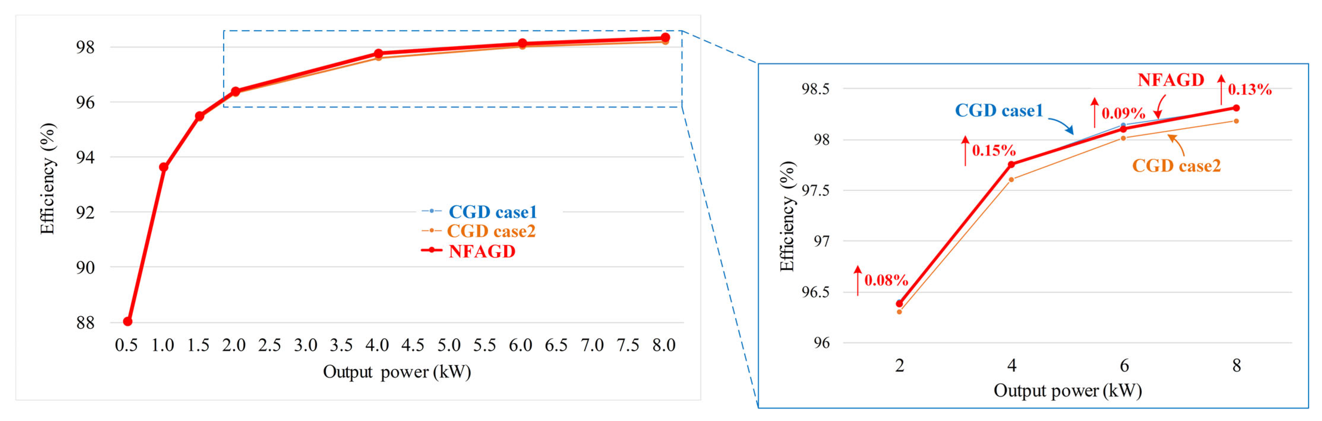
4.2. Synchronous Buck Converter Prototype Verification

A synchronous buck converter experimental prototype was built to further verify the effectiveness of the proposed NFAGD application strategy for parallel SiC MOSFETs in a converter, as shown in Figure 12b. To further verify the effectiveness of the proposed NFAGD application strategy for parallel SiC MOSFETs in a converter, a synchronous buck converter experimental prototype was built, as shown in Figure 12b. The input is 800 V, and the output is 400 V. The converter operates under a 30 kHz switching frequency with an 8 kW rated power. The converter’s devices are connected in parallel and implemented with SiC MOSFET IMZ120R045M1, as used in the analysis and double-pulse test above.
Figure 16 compares synchronous buck converter efficiencies under three gate drive strategies: CGD Case 1, CGD Case 2, and NFAGD. During the efficiency test, different gate driver boards were used to change the gate drive strategies, while the power loop, control circuits, and PCB layout were the same. Gate driver boards were the only modified element.
As it is shown in Figure 16, the converter under the proposed NFAGD application strategy has a similar efficiency to CGD Case 1 across the entire operation range, due to the similar switching speeds of the two gate drives. Compared to CGD Case 2, the converter shows an efficiency improvement of about 0.08% at a light load of 2 kW under the drive of the proposed NFAGD application strategy, saving about 1.6 W switching loss; at a half load of 4 kW, the NFAGD converter has an efficiency improvement of about 0.15%, saving about 6 W switching loss; at full load 8 kW, the converter shows an efficiency improvement of about 0.13% under the drive of the proposed NFAGD application strategy, saving about 10.4 W switching loss.
The switching waveforms of the proposed NFAGD in Figure 15 and its counterpart CGD Case 2 in Figure 14b, which can be treated as the testing waveforms under the full-load 8 kW condition, are compared to evaluate the switching loss. The switching loss corresponding to the higher dv/dt condition in Figure 15 is about 43.2 W, and the switching loss corresponding to the lower dv/dt condition in Figure 14b is about 54.72 W. Based on this calculation, the reduced switch loss means a 0.14% efficiency improvement with the proposed NFAGD, which copes with the efficiency test results in Figure 16, where a 0.13% increase is shown at 8 kW. The proposed NFAGD has a larger dv/dt than that in CGD Case 2. Hence, the switching loss would be reduced by using the proposed NFAGD. Thus, the efficiency is improved.
Comparing the switching waveforms of the proposed NFAGD in Figure 15 and its counterpart CGD Case 1 in Figure 13b, their dv/dt is similar, so their switching loss is similar, and their efficiency is similar, as shown in Figure 16. The efficiency of the NFAGD is not reduced. Considering the theoretical analysis in Section 3 and the double-pulse test results in Section 4.1, the proposed NFAGD can bypass interference sources through negative feedback automatic control. This strategy automatically suppresses crosstalk parasitic oscillation, thereby achieving voltage stability.
In sum, the efficiency comparison experiments under different gate drive circuits demonstrate that the proposed NFAGD application strategy for parallel SiC MOSFETs is suitable for systematic application, as it suppresses the crosstalk parasitic oscillation without reducing efficiency.

5. Conclusions

This paper proposes a Negative Feedback Active Gate Drive (NFAGD) application strategy for parallel SiC MOSFETs to avoid gate voltage stress without decreasing efficiency. This strategy would fill the lack of active gate drive control in the systematic converter with parallel SiC MOSFETs because the crosstalk parasitic oscillation makes it challenging to control in a power converter with SiC MOSFETs switching at high dv/dt over 20 V/ns. This paper investigates a dynamic model for gate voltage-interfered oscillation in parallel SiC MOSFETs. It shows that the gate voltage interference path becomes complex and sensitive to the influence of parasitic stray parameters. The dynamic model also makes it possible to mathematically analyze the operation principle of the proposed NFAGD application strategy. Based on the dynamic model, the operation principle of the proposed NFAGD application strategy is given. The double-pulse test results demonstrate that this strategy can effectively suppress crosstalk parasitic oscillation without sacrificing the switching speed of SiC MOSFETs, decreasing about 70% of the peak-to-peak crosstalk parasitic oscillation. The speed/crosstalk ratio can be increased to KSC = 17.98, indicating that the efficiency would have a low probability of being impacted in the systematic converter application with this gate drive. An 8 kW synchronous buck converter prototype was built, and efficiency comparison experiments under different gate drive circuits demonstrate that the proposed NFAGD application strategy for parallel SiC MOSFETs is suitable for systematic application, as it suppresses the crosstalk parasitic oscillation without reducing efficiency, and even increases the efficiency by about 0.08~0.13%.

Author Contributions

Conceptualization, T.S. and T.Q.Z.; methodology, T.S.; software, Z.B.; validation, T.S., Y.S. and Z.B.; formal analysis, Y.Z.; investigation, T.S.; resources, T.Q.Z.; data curation, P.J.; writing—original draft preparation, Y.S.; writing—review and editing, T.S.; visualization, Z.B.; supervision, T.Q.Z.; project administration, Y.Z.; funding acquisition, P.J. All authors have read and agreed to the published version of the manuscript.

Funding

This work was supported in part by the General Programs of the National Natural Science Foundation of China under Grant 52377165, in part by the Beijing Natural Science Foundation under Grant 3232044 and the National Natural Science Foundation of China under Grant 52237008.

Data Availability Statement

Data are contained within the article.

Conflicts of Interest

The authors declare no conflicts of interest.

Nomenclature

NFAGDNegative feedback active gate drive.
Q1, Q2Passive devices
Q3, Q4Active devices
QP1, QP2P-channel auxiliary MOSFETs
vdisDisturbance voltage source
vGS*Gate drive signal
R1, R2, R3, R4External gate drive resistances
LσPower loop inductance
Rg1, Rg2Internal gate resistances
Ciss1, Ciss2Input capacitance
Lg1, Lg2Drive stray inductance
LKS1, LKS2Kelvin stray inductance
LoD1, LoD2Drain stray inductance
LoS1, LoS2Source stray inductance
gm1, gm2Transconductance of QP1 and QP2
KSCSpeed/crosstalk ratio

References

  1. Zeng, Z.; Shao, W.; Hu, B.; Chen, H.; Liao, X.; Chen, W.; Li, H.; Ran, L. Chances and challenges of photovoltaic inverters with silicon carbide devices. Renew. Sustain. Energy Rev. 2017, 78, 624–639. [Google Scholar] [CrossRef]
  2. Qian, Z.; Zhang, J.; Sheng, K. Status and Development of Power Semiconductor Devices and Its Applications. Proc. CSEE 2014, 34, 5149–5161. [Google Scholar]
  3. Sheng, K.; Ren, N.; Xu, H. A Recent Review on Silicon Carbide Power Devices Technologies. Proc. CSEE 2020, 40, 1735–1741. [Google Scholar]
  4. Wang, F.; Zhang, Z. Overview of Silicon Carbide Technology: Device, Converter, System, and Application. CPSS Trans. Power Electron. Appl. 2016, 1, 13–32. [Google Scholar] [CrossRef]
  5. Shi, B.; Zhao, Z.; Jiang, Y.; Zhu, Y. Multi-Time Scale Transient Models for Power Semiconductor Devices (Part I: Switching Characteristics and Transient Modeling). Trans. China Electrotech. Soc. 2017, 32, 16–24. [Google Scholar]
  6. Jiang, Y.; Zhao, Z.; Shi, B.; Yuan, L. Multi-Time Scale Transient Models for Power Semiconductor Devices (Part II: Applications Analysis and Model Connection). Trans. China Electrotech. Soc. 2017, 32, 25–32. [Google Scholar]
  7. He, J.; Liu, Y.; Bi, D.; Li, X. Impacts of Voltage Probes for Accurate Measurement of High-Frequency Transient Voltage of Wide-Bandgap Devices. Trans. China Electrotech. Soc. 2021, 36, 362–372. [Google Scholar]
  8. Schrittwieser, L.; Leibl, M.; Haider, M.; Thöny, F.; Kolar, J.W.; Soeiro, T.B. 99.3% efficient three-phase buck-type all-SiC SWISS rectifier for DC distribution systems. IEEE Trans. Power Electron. 2019, 34, 126–140. [Google Scholar] [CrossRef]
  9. Li, Y.; Liang, M.; Chen, J.; Zheng, T.Q.; Guo, H. A Low Gate Turn–OFF Impedance Driver for Suppressing Crosstalk of SiC MOSFET Based on Different Discrete Packages. IEEE J. Emerg. Sel. Top. Power Electron. 2019, 7, 353–365. [Google Scholar] [CrossRef]
  10. Li, H.; Qiu, Z.; Shao, T.; Zeng, Y.; Du, H.; Yin, C. A Low Level–Clamped Active Gate Driver for Crosstalk Suppression of SiC MOSFET Based on dv/dt Detection. In Proceedings of the 2021 IEEE Energy Conversion Congress and Exposition (ECCE), Vancouver, BC, Canda, 10–14 October 2021; pp. 5348–5353. [Google Scholar]
  11. Li, H.; Jiang, Y.; Qiu, Z.; Shao, T.; Wang, Y. A Multi-step Active Gate Driver for Suppressing Crosstalk of SiC MOSFET. In Proceedings of the 2020 IEEE 9th International Power Electronics and Motion Control Conference (IPEMC2020-ECCE Asia), Nanjing, China, 29 November–2 December 2020. [Google Scholar]
  12. Qiu, Z.; Li, H.; Jiang, Y.; Shao, T.; Yang, Z.; Wang, J.; Zhang, Z. An Intelligent Three-level Active Gate Driver for Crosstalk Suppression of SiC MOSFET. In Proceedings of the Twelfth Annual IEEE Energy Conversion Congress and Exposition (ECCE 2020), Detroit, MI, USA, 10–15 October 2020. [Google Scholar]
  13. Zhang, Z.; Dix, J.; Wang, F.; Blalock, B.J.; Costinett, D.; Tolbert, L.M. Intelligent Gate Drive for Fast Switching and Crosstalk Suppression of SiC Devices. IEEE Trans. Power Electron. 2017, 32, 9319–9332. [Google Scholar] [CrossRef]
  14. Aichinger, T.; Rescher, G.; Pobegen, G. Threshold Voltage Peculiarities and Bias Temperature Instabilities of SiC MOSFETs. Microelectron. Reliab. 2018, 80, 68–78. [Google Scholar] [CrossRef]
  15. Yu, H.; Liang, S.; Liu, H.; Wang, J.; Shen, Z.J. Numerical Study of SiC MOSFET With Integrated n-/n-Type Poly-Si/SiC Heterojunction Freewheeling Diode. IEEE Trans. Electron Devices 2021, 68, 4571–4576. [Google Scholar] [CrossRef]
  16. Peters, D.; Aichinger, T.; Basler, T.; Rescher, G.; Puschkarsky, K.; Reisinger, H. Investigation of Threshold Voltage Stability of SiC MOSFETs. In Proceedings of the 2018 IEEE 30th International Symposium on Power Semiconductor Devices and ICs (ISPSD), Chicago, IL, USA, 13–17 May 2018; pp. 40–43. [Google Scholar]
  17. Burkart, R.M.; Kolar, J.W. Comparative Life Cycle Costs Analysis of Si and SiC PV Converter Systems Based on Advanced η-ρ-σ Multi–Objective Optimization Techniques. IEEE Trans. Power Electron. 2017, 32, 4344–4358. [Google Scholar] [CrossRef]
  18. Burkart, R.M.; Kolar, J.W. Comparative η–ρ–σ Pareto Optimization of Si and SiC Multilevel Dual-Active-Bridge Topologies With Wide Input Voltage Range. IEEE Trans. Power Electron. 2017, 32, 5258–5270. [Google Scholar] [CrossRef]
  19. Ba, T.; Li, Y.; Liang, M. The Effect of Parasitic Parameters on Gate–Source Voltage of SiC MOSFET. Trans. China Electrotech. Soc. 2016, 31, 64–73. [Google Scholar]
  20. Duan, Z.; Zhang, D.; Fan, T. Modeling and Prediction of Electromagnetic Interference in SiC Motor Drive Systems. Trans. China Electrotech. Soc. 2020, 35, 4726–4738. [Google Scholar]
  21. Zhang, Z.; Guo, B.; Wang, F.F.; Jones, E.A.; Tolbert, L.M.; Blalock, B.J. Methodology for Wide Band-Gap Device Dynamic Characterization. IEEE Trans. Power Electron. 2017, 32, 9307–9318. [Google Scholar] [CrossRef]
  22. Chen, J.; Du, X.; Luo, Q.; Zhang, X.; Sun, P.; Zhou, L. A Review of Switching Oscillations of Wide Bandgap Semiconductor Devices. IEEE Trans. Power Electron. 2020, 35, 13182–13199. [Google Scholar] [CrossRef]
  23. Wang, X.; Zhu, Y.; Zhao, Z.; Chen, K. Impact of Gate-Loop Parameters on the Switching Behavior of SiC MOSFETs. Trans. China Electrotech. Soc. 2017, 32, 23–30. [Google Scholar]
  24. Zhang, W.; Huang, X.; Lee, F.C.; Li, Q. Gate Drive Design Considerations for High Voltage Cascode GaN HEMT. In Proceedings of the 2014 IEEE Applied Power Electronics Conference and Exposition–APEC 2014, Fort Worth, TX, USA, 16–20 March 2014; pp. 1484–1489. [Google Scholar]
  25. Liu, P.; Guo, S.; Yu, R.; Huang, A.Q.; Zhang, L. Analysis of Trade-Off Between Noise and Wide Band-Gap (WBG) Device Switching Speed. In Proceedings of the 2018 IEEE Energy Conversion Congress and Exposition (ECCE), Portland, OR, USA, 23–27 September 2018; pp. 3483–3489. [Google Scholar]
  26. Yang, X.; Li, J.; Ding, Y.; Xu, M.; Zhu, X.; Zhu, J. Observation of Transient Parity-Time Symmetry in Electronic Systems. Phys. Rev. Lett. 2022, 128, 065701. [Google Scholar] [CrossRef]
  27. Yang, X.; Yuan, Y.; Long, Z.; Goncalves, J.; Palmer, P.R. Robust Stability Analysis of Active Voltage Control for High-power IGBT Switching by Kharitonov’s Theorem. IEEE Trans. Power Electron. 2016, 31, 2584–2595. [Google Scholar] [CrossRef]
  28. Wang, K.; Yang, X.; Wang, L.; Jain, P. Instability Analysis and Oscillation Suppression of Enhancement-Mode GaN Devices in Half-Bridge Circuits. IEEE Trans. Power Electron. 2018, 33, 1585–1596. [Google Scholar] [CrossRef]
  29. Zeng, Z.; Li, X. Comparative Study on Multiple Degrees of Freedom of Gate Drivers for Transient Behavior Regulation of SiC MOSFET. IEEE Trans. Power Electron. 2018, 33, 8754–8763. [Google Scholar] [CrossRef]
  30. Zhu, T.; Zhuo, F.; Zhao, F.; Wang, F.; Zhao, T. Quantitative Model-Based False Turn-on Evaluation and Suppression for Cascode GaN Devices in Half-Bridge Applications. IEEE Trans. Power Electron. 2019, 34, 10166–10179. [Google Scholar] [CrossRef]
  31. Zhang, Z.; Wang, F.; Tolbert, L.M.; Blalock, B.J. Active Gate Driver for Crosstalk Suppression of SiC Devices in a Phase-Leg Configuration. IEEE Trans. Power Electron. 2014, 29, 1986–1997. [Google Scholar] [CrossRef]
  32. Zhao, S.; Dearien, A.; Wu, Y.; Farnell, C.; Rashid, A.U.; Luo, F.; Mantooth, H.A. Adaptive Multi-Level Active Gate Drivers for SiC Power Devices. IEEE Trans. Power Electron. 2020, 35, 1882–1898. [Google Scholar] [CrossRef]
  33. STMicroelectronics AN-5355, Mitigation Technique of the SiC MOSFET Gate Voltage Glitches with Miller Clamp. 2019. Available online: https://www.st.com/resource/en/application_note/dm00628522-mitigation-technique-of-the-sic-mosfet-gate-voltage-glitches-with-miller-clamp-stmicroelectronics.pdf (accessed on 15 February 2025).
  34. Avago Technologies AN-5314, Active Miller Clamp. 2010. Available online: https://docs.broadcom.com/doc/AV02-0072EN (accessed on 15 February 2025).
  35. Shao, T.; Zheng, T.Q.; Li, H.; Liu, J.; Li, Z.; Huang, B.; Qiu, Z. The Active Gate Drive Based on Negative Feedback Mechanism for Fast Switching and Crosstalk Suppression of SiC Devices. IEEE Trans. Power Electron. 2022, 37, 6739–6754. [Google Scholar] [CrossRef]
  36. Shao, T.; Zheng, T.Q.; Li, Z.; Li, H.; Liu, J. SiC MOSFET Gate Driver Design Based on Interference Dynamic Response Mechanism. Trans. China Electrotech. Soc. 2021, 36, 4204–4214. [Google Scholar]
  37. JESD24; Power MOSFETs. JEDEC: Arlington, VA, USA, 1985.
  38. Gao, Y.; Chen, Q. Silicon Carbide Power Semiconductor Devices: Characteristics, Testing and Applications; China Machine Press: Beijing, China, 2021. [Google Scholar]
Figure 1. Equivalent circuit in the phase-leg configuration with paralleled devices under conventional gate drive (CGD).
Electronics 14 02100 g001
Figure 2. Schematic diagram of waveforms in parallel phase-leg configuration.
Electronics 14 02100 g002
Figure 3. Simplified equivalent circuit for power loop: (a) before decoupling, (b) after decoupling.
Electronics 14 02100 g003
Figure 4. Equivalent path from the disturbance vdis to gate voltages vGS1 and vGS2.
Electronics 14 02100 g004
Figure 5. Equivalent path for the drive signal vGS*.
Electronics 14 02100 g005
Figure 6. Block diagram of transfer function for gate voltage interference path in parallel devices.
Electronics 14 02100 g006
Figure 7. Amplitude of the transfer function of gate voltage disturbances in parallel devices.
Electronics 14 02100 g007
Figure 8. Effect of different power stray inductance on gate voltage disturbances in parallel devices.
Electronics 14 02100 g008
Figure 9. Parallel devices vs. single device.
Electronics 14 02100 g009
Figure 10. Negative Feedback Active Gate Drive (NFAGD) application strategy for parallel SiC MOSFETs.
Electronics 14 02100 g010
Figure 11. The feedback control loop of the gate drive.
Electronics 14 02100 g011
Figure 12. Outlook of the experimental platforms: (a) the double-pulse test platform, (b) the synchronous buck converter experimental prototype.
Electronics 14 02100 g012
Figure 13. Double-pulse test results of CGD Case 1: (a) single device, (b) parallel devices.
Electronics 14 02100 g013
Figure 14. Double-pulse test results of CGD Case 2: (a) single device, (b) parallel devices.
Electronics 14 02100 g014
Figure 15. NFAGD waveforms for parallel devices.
Electronics 14 02100 g015
Figure 16. Efficiency test results of the synchronous buck converter prototype.
Electronics 14 02100 g016
Table 1. The features of different drive methods.
Drive MethodTypical Max. dv/dtInfluence of Switching Speed 1Typical Gate Parasitic Oscillation 2Speed/Crosstalk Ratio KSCConstitutive
Complexity 3
Conventional Gate Drive (CGD) [29]35 V/ns100%6.6 V @36.78 V/ns5.572 devices: 1R, 1 IC
Gate Impedance Regulation (GIR) [31]25 V/ns 71%1.5 V @24.4 V/ns [31]16.27 [31]5 devices: 1R, 2 IC, 1 SW, 1 C
Gate Voltage Control (GVC) [31]25 V/ns 71%3.2 V @24.9 V/ns [31]7.78 [31]7 devices: 1R, 3 IC, 2 SW, 1 D
Intelligent Gate Drive (IGD) [13]20 V/ns57%4.16 V @22 V/ns [13]5.29 [13]8 devices: 1R, 3 IC, 2 SW, 2 D
Multi-level Active Gate Driver [32]10 V/ns29%10 V @10.7 V/ns [32]1.07 [32]7 devices: 1R, 2 IC, 4 SW
Active Miller Clamp (AMC) [15,33]20 V/ns57%10 V @30 V/ns [33]3 [33]7 devices: 1R, 2 IC, 4 SW
Negative Feedback Active Gate Drive (NFAGD) 40 V/ns114%2 V @35.95 V/ns17.984 devices: 1R, 1 IC, 1 SW, 1C
Note 1: The switching speed comparison takes CGD dv/dt as the base. Note 2: The peak-to-peak crosstalk parasitic oscillation is taken from the experimental results inside the references. Note 3: R denotes drive resistors, C denotes auxiliary capacitors, SW denotes auxiliary switch devices, D denotes auxiliary diodes, and IC denotes driver ICs.
Table 2. The SiC MOSFET parameters used for analysis.
ParametersSymbolsType Values
Input CapacitanceCiss1900 pF
Output CapacitanceCoss115 pF
Reverse Transmission CapacitanceCrss13 pF
Gate Internal ResistorRg4 Ω
Table 3. Experimental parameters.
ParametersValues/Type
Turn-on bias voltage (VCC)15 V
Turn-off bias voltage (VEE)−4 V
CGD Case 1: drive resistance10 Ω
CGD Case 2: drive resistance15 Ω
NFAGD: drive resistance1.65 Ω
NFAGD: auxiliary MOSFET (QP)BSO201SP
NFAGD: auxiliary capacitor (Ca)10 nF
Disclaimer/Publisher’s Note: The statements, opinions and data contained in all publications are solely those of the individual author(s) and contributor(s) and not of MDPI and/or the editor(s). MDPI and/or the editor(s) disclaim responsibility for any injury to people or property resulting from any ideas, methods, instructions or products referred to in the content.

