
Initial/Last-State-Correlated SAR Control with Optimized Trajectory to Reduce Reverse Overshoot and Smooth Current Switching of Hybrid LDOs

 , ,
, ,
Abstract
1. Introduction
2. Operating Principles of a Conventional SAR Controller in Hybrid LDO
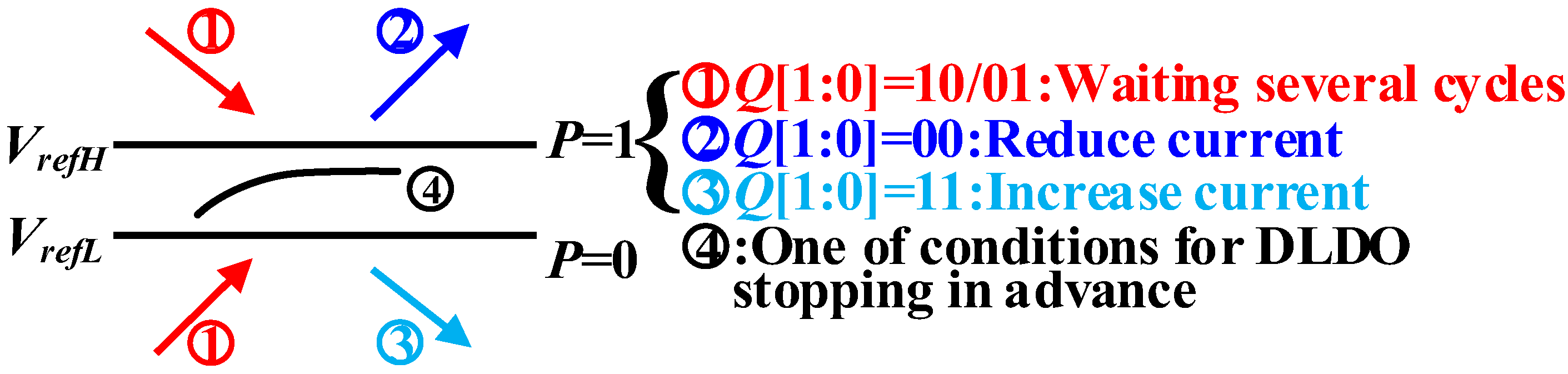
2.1. Adjusting Process of Conventional SAR Controller
- P = 1: The SAR controller continues to adjust the output current.
- P = 0: This represents one of the conditions for DLDO stopping operation in advance.
- Q [1:0] = 10/01: The SAR controller waits for several clock cycles.
- Q [1:0] = 11: The SAR controller regulates the DLDO to increase the output current.
- Q [1:0] = 00: The SAR controller regulates the DLDO to reduce the output current.
2.2. Current Switching of Conventional SAR Controller with CLASS-D
3. Optimized Trajectory of Initial/Last-State Correlated SAR Controller with ALDO
3.1. Trajectory of the SAR Controller with CLASS-D
3.2. Optimized Trajectory of the Initial/Last-State-Correlated SAR with ALDO
4. Design Difficulties of Optimized Trajectory Implementation in Hybrid LDO
- The waiting cycle number and threshold width need to be precisely calculated to attain the specific stable state.
- The current switching logic needs to be designed to smooth the output voltage response.
- The compensation resistance RM needs to be accurately derived under different load conditions to achieve adaptive miller compensation.
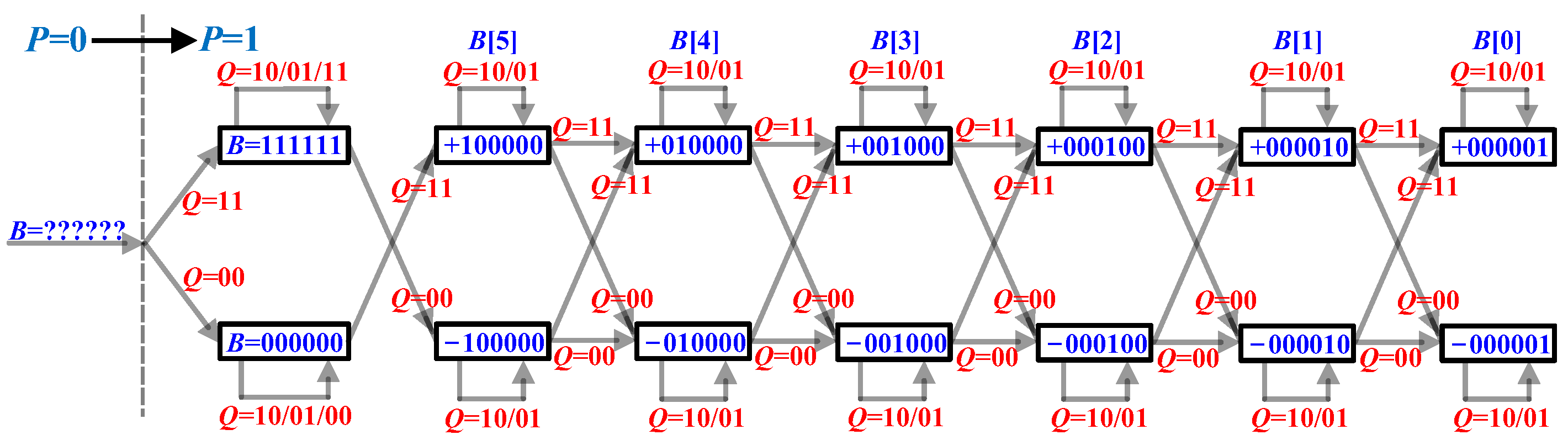
4.1. Waiting Cycle Number and Threshold Width
- Threshold width: After the proposed SAR control, the output voltage can achieve into the hysteresis region. Considering output current capacity of the ALDO, the hysteresis region can only contain a specific stable state. However, with the ending position setting logic, the stable state N = Nspecific + 1 can be adjusted to the specific stable state. Therefore, the threshold region can contain less than three stable states, and the threshold width satisfies Vw < 2I0RL, MIM.
- Waiting cycle number: In Figure 14, the output voltage of Track II and Track III can converge to V3 and V4, with ALDO capable of adjusting the output voltage to the reference voltage. For all other tracks, Track I and Track IV are closest to Track II and Track III. Therefore, Track I and Track IV are most difficult to distinguish from Track II and Track III. For Track I and Track II, the output voltage of Track II needs to achieve V2 so as to distinguish Track I and Track II.
4.2. Current Switching Logic
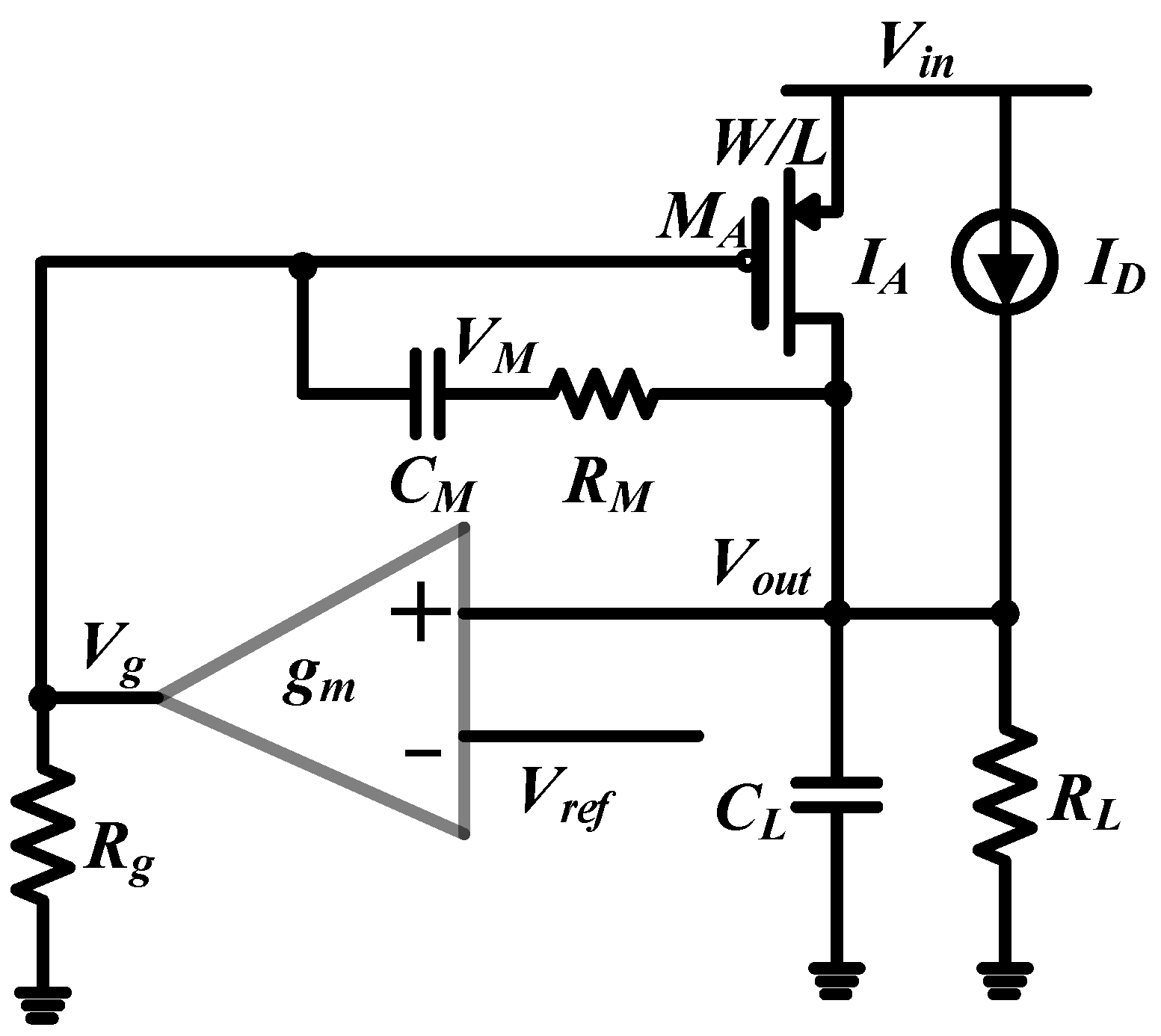
4.3. RM Design in the Adaptive Miller Compensation According to the Load Range
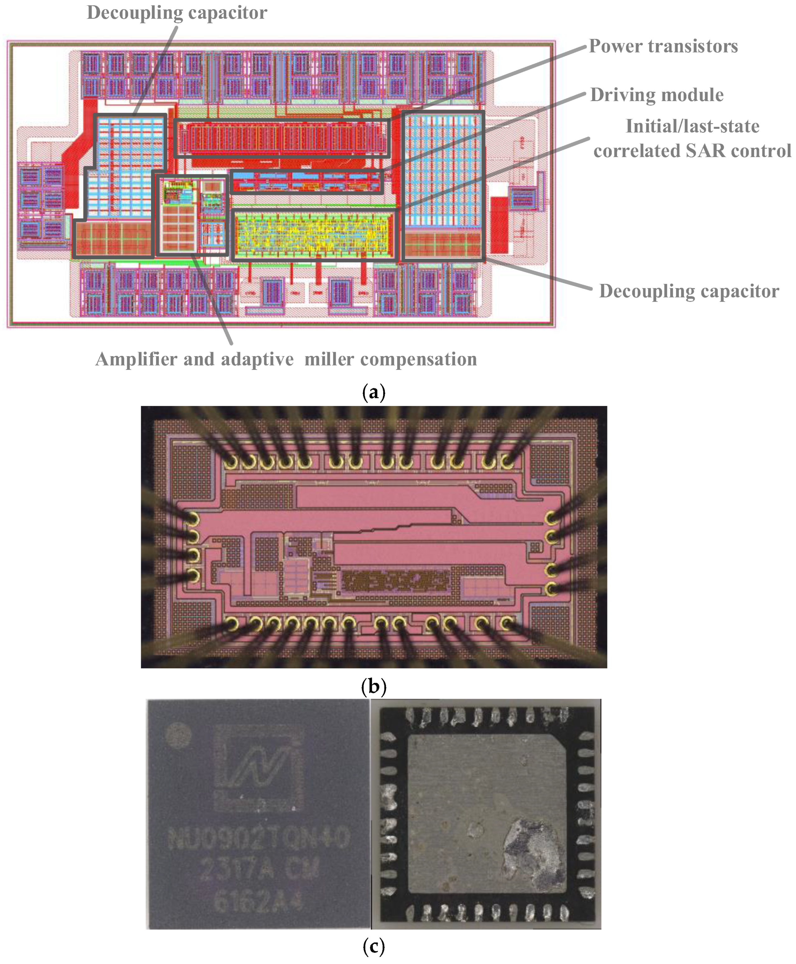
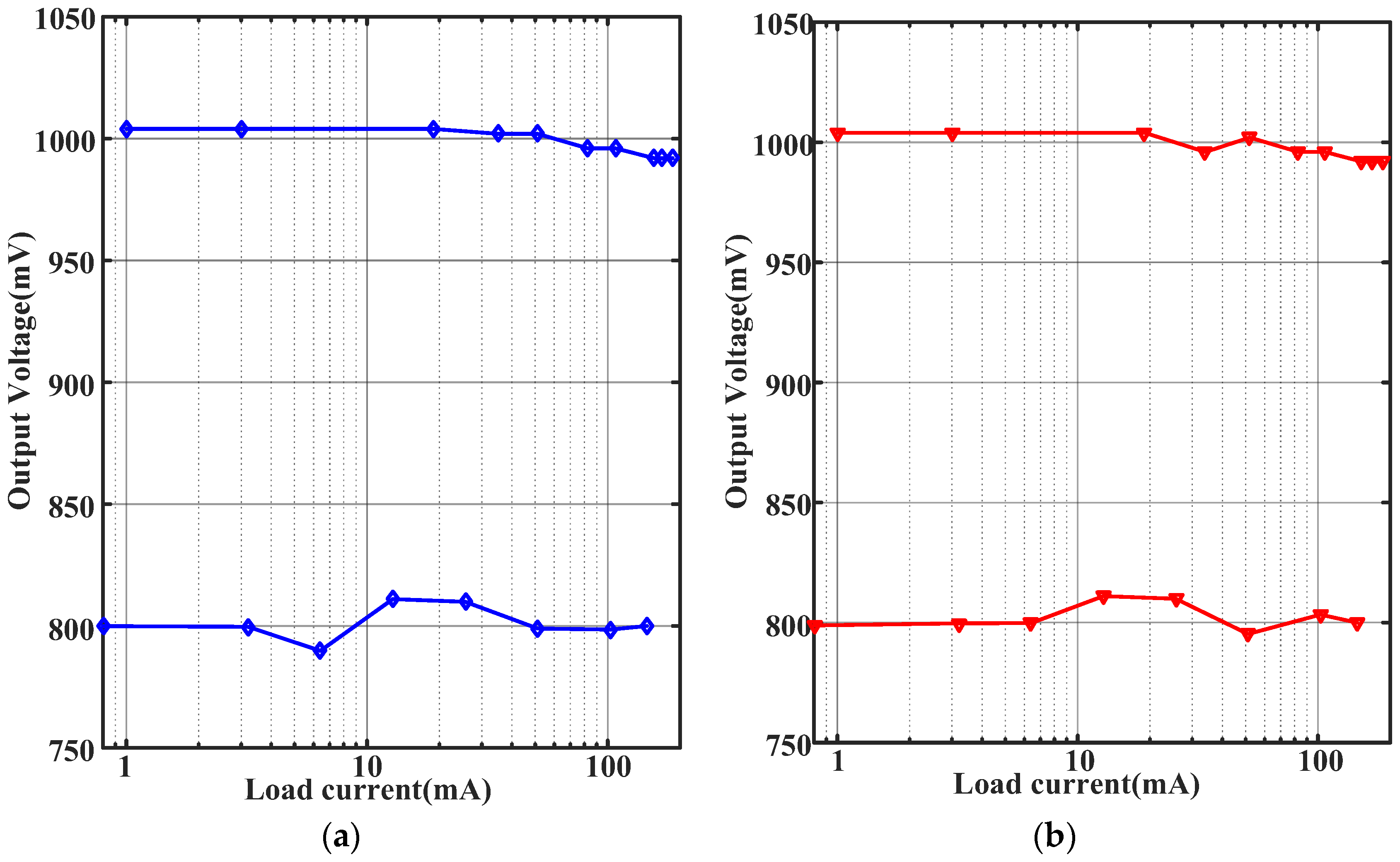
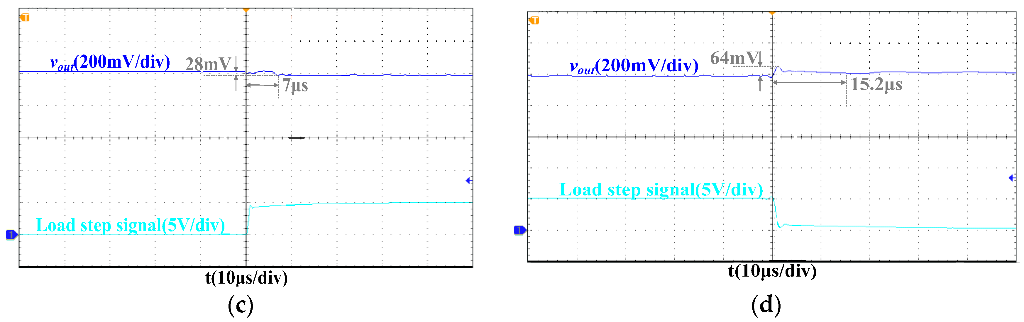
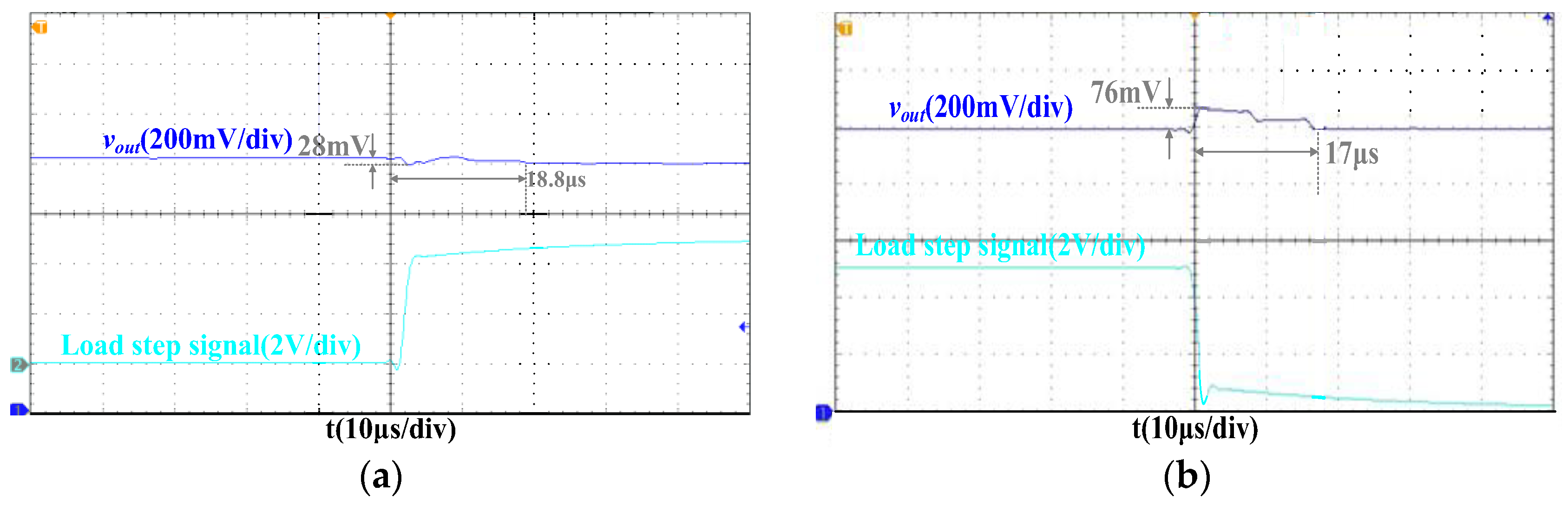
5. Layout and Experiment
6. Conclusions
Author Contributions
Funding
Data Availability Statement
Conflicts of Interest
References
- Lee, Y.J.; Jung, M.Y.; Singh, S.; Kong, T.H.; Kim, D.Y.; Kim, K.H.; Kim, S.H.; Park, J.J.; Park, H.J.; Cho, G.H. A 200mA digital low-drop-out regulator with coarse-fine dual loop in mobile application processors. In Proceedings of the 2016 IEEE International Solid-State Circuits Conference (ISSCC), San Francisco, CA, USA, 31 January–4 February 2016; pp. 150–151. [Google Scholar]
- Liu, X.; Krishnamurthy, H.K.; Na, T.; Weng, S.; Ahmed, K.Z.; Ravichandran, K.; Tschanz, J.; De, V. A Modular Hybrid LDO with Fast Load-Transient Response and Programmable PSRR in 14nm CMOS Featuring Dynamic Clamp Tuning and Time-Constant Compensation. In Proceedings of the 2019 IEEE International Solid-State Circuits Conference (ISSCC), San Francisco, CA, USA, 17–21 February 2019; pp. 234–236. [Google Scholar]
- Tsou, W.J.; Yang, W.H.; Lin, J.H.; Chen, H.; Chen, K.H.; Wey, C.L.; Lin, Y.H.; Lin, S.R.; Tsai, T.Y. Digital low-dropout regulator with anti PVT-variation technique for dynamic voltage scaling and adaptive voltage scaling multicore processor. In Proceedings of the 2017 IEEE International Solid-State Circuits Conference (ISSCC), San Francisco, CA, USA, 5–9 February 2017; pp. 338–339. [Google Scholar]
- Kim, S.; Shih, Y.-C.; Mazumdar, K.; Jain, R.; Ryan, J.; Tokunaga, C.; Augustine, C.; Kulkarni, J.; Ravichandran, K.; Tschanz, J.; et al. Enabling wide autonomous DVFS in a 22nm graphics execution core using a digitally controlled hybrid LDO/switched-capacitor VR with fast droop mitigation. In Proceedings of the 2015 IEEE International Solid-State Circuits Conference (ISSCC) Digest of Technical, San Francisco, CA, USA, 22–26 February 2015. [Google Scholar]
- Chen, F.; Lu, Y.; Mok, P.K.T. A Fast-Transient 500-mA Digitally Assisted Analog LDO With 30-μ V/mA Load Regulation and 0.0073-ps FoM in 65-nm CMOS. IEEE J. Solid State Circuits 2021, 56, 511–520. [Google Scholar] [CrossRef]
- Yang, F.; Mok, P.K.T. A Nanosecond-Transient Fine-Grained Digital LDO With Multi-Step Switching Scheme and Asynchronous Adaptive Pipeline Control. IEEE J. Solid State Circuits 2017, 52, 2463–2474. [Google Scholar] [CrossRef]
- Jayaraman, K.; Rawy, K.; Kim, T.T.-H. A 0.6-V power efficient digital LDO with 99.7% current efficiency utilizing load current aware clock modulation for fast transient response. In Proceedings of the 2016 IEEE Asia Pacific Conference on Circuits and Systems (APCCAS), Jeju, Republic of Korea, 25–28 October 2016; pp. 103–106. [Google Scholar]
- Anusha, G.; Kumar, A.; Kandpal, K. A Fully On-Chip Low-Dropout Regulator for SoC applications. Procedia Comput. Sci. 2020, 171, 1009–1017. [Google Scholar] [CrossRef]
- Oh, J.; Park, J.E.; Hwang, Y.H.; Jeong, D.K. A 480mA Output-Capacitor-Free Synthesizable Digital LDO Using CMP-Triggered Oscillator and Droop Detector with 99.99% Current Efficiency, 1.3ns Response Time, and 9.8A/mm2 Current Density. In Proceedings of the 2020 IEEE International Solid- State Circuits Conference (ISSCC), San Francisco, CA, USA, 16–20 February 2020; pp. 382–384. [Google Scholar]
- Lo, Y.-L.; Chen, W.-J. A 0.7 V input output-capacitor-free digitally controlled low-dropout regulator with high current efficiency in 0.35 μm CMOS technology. Microelectron. J. 2012, 43, 756–765. [Google Scholar] [CrossRef]
- Nasir, S.B.; Sen, S.; Raychowdhury, A. Switched-Mode-Control Based Hybrid LDO for Fine-Grain Power Management of Digital Load Circuits. IEEE J. Solid State Circuits 2018, 53, 569–581. [Google Scholar] [CrossRef]
- Zhang, Y.; Zhao, X.; Wang, Y.; Dong, L. A fully integrated overshoot-reduction low-dropout regulator based on hybrid NMOS/PMOS power transistors technique for SoC applications. Microelectron. J. 2022, 125, 105471. [Google Scholar] [CrossRef]
- Salem, L.G.; Warchall, J.; Mercier, P.P. A Successive Approximation Recursive Digital Low-Dropout Voltage Regulator With PD Compensation and Sub-LSB Duty Control. IEEE J. Solid State Circuits 2018, 53, 35–49. [Google Scholar] [CrossRef]
- Nasir, S.B.; Gangopadhyay, S.; Raychowdhury, A. A 0.13 μm fully digital low-dropout regulator with adaptive control and reduced dynamic stability for ultra-wide dynamic range. In Proceedings of the 2015 IEEE International Solid-State Circuits Conference (ISSCC) Digest of Technical Papers, San Francisco, CA, USA, 22–26 February 2015; pp. 1–3. [Google Scholar]
- Li, S.; Calhoun, B.H. A 745 pA Hybrid Asynchronous Binary-Searching and Synchronous Linear-Searching Digital LDO with 3.8 × 10⁵ Dynamic Load Range, 99.99% Current Efficiency, and 2 mV Output Voltage Ripple. In Proceedings of the 2019 IEEE International Solid- State Circuits Conference (ISSCC), San Francisco, CA, USA, 17–21 February 2019; pp. 232–234. [Google Scholar]
- Akram, M.A.; Hong, W.; Hwang, I. Capacitorless Self-Clocked All-Digital Low-Dropout Regulator. IEEE J. Solid State Circuits 2019, 54, 266–276. [Google Scholar] [CrossRef]
- Ma, X.; Lu, Y.; Martins, R.P.; Li, Q. A 0.4 V 430 nA quiescent current NMOS digital LDO with NAND-based analog-assisted loop in 28 nm CMOS. In Proceedings of the 2018 IEEE International Solid State Circuits Conference (ISSCC), San Francisco, CA, USA, 11–15 February 2018; pp. 306–308. [Google Scholar]
- Xu, W.; Upadhyaya, P.; Wang, X.; Tsang, R.; Lin, L. A 1A LDO regulator driven by a 0.0013 mm2 Class-D controller. In Proceedings of the 2017 IEEE International Solid-State Circuits Conference (ISSCC), San Francisco, CA, USA, 5–9 February 2017; pp. 104–105. [Google Scholar]
- Jooq, M.K.Q.; Moaiyeri, M.H.; Al-Shidaifat, A.; Song, H. Ultra-Efficient and Robust Auto-Nonvolatile Schmitt Trigger-Based Latch Design Using Ferroelectric CNTFET Technology. IEEE Trans. Ultrason. Ferroelectr. Freq. Control 2022, 69, 1829–1840. [Google Scholar] [CrossRef] [PubMed]
- Huang, M.; Lu, Y.; U, S.-P.; Martins, R.P. An Analog-Assisted Tri-Loop Digital Low-Dropout Regulator. IEEE J. Solid State Circuits 2018, 53, 20–34. [Google Scholar] [CrossRef]
- Nasir, S.; Sen, S.; Raychowdhury, A. A Reconfigurable Hybrid Low Dropout Voltage Regulator for Wide-Range Power Supply Noise Rejection and Energy-Efficiency Trade-Off. IEEE Trans. Circuits Syst. II Express Briefs 2018, 65, 1864–1868. [Google Scholar] [CrossRef]


| Output Voltage Level | Changing Direction | P | Q [1] | Q [0] |
|---|---|---|---|---|
| VrefL < Vout < VrefH | × | 0 | × | × |
| Vout < VrefL | ↑ | 1 | 1 | 0 |
| Vout < VrefL | ↓ | 1 | 1 | 1 |
| Vout > VrefH | ↑ | 1 | 0 | 0 |
| Vout > VrefH | ↓ | 1 | 0 | 1 |
| VIN | Vref | I0 | fCLK | CL | VrefH | VrefL |
|---|---|---|---|---|---|---|
| 1.8 V | 1 V | 5 mA | 50 MHz | 100 nF | 1.01 V | 0.99 V |
| Initial State | Q | Starting Position |
|---|---|---|
| 000000–011111 | 11 | 100000 (>last state) |
| 100000–111111 | 11 | 111111 (>last state) |
| 000000–011111 | 00 | 000000 (<last state) |
| 100000–111111 | 00 | 011111 (<last state) |
| Q | Ending Position | Gate Volatge |
|---|---|---|
| 11 | Last state | 0 |
| 00 | Last state-6′b000001 | VDD |
| Differential Equation | Discrete Form | Calculated Quantity |
|---|---|---|
| Control Methods | Conventional SAR | Proposed SAR | ||
|---|---|---|---|---|
| Load step (Ω) | 100→3.5 | 100→35 | 100→3.5 | 100→35 |
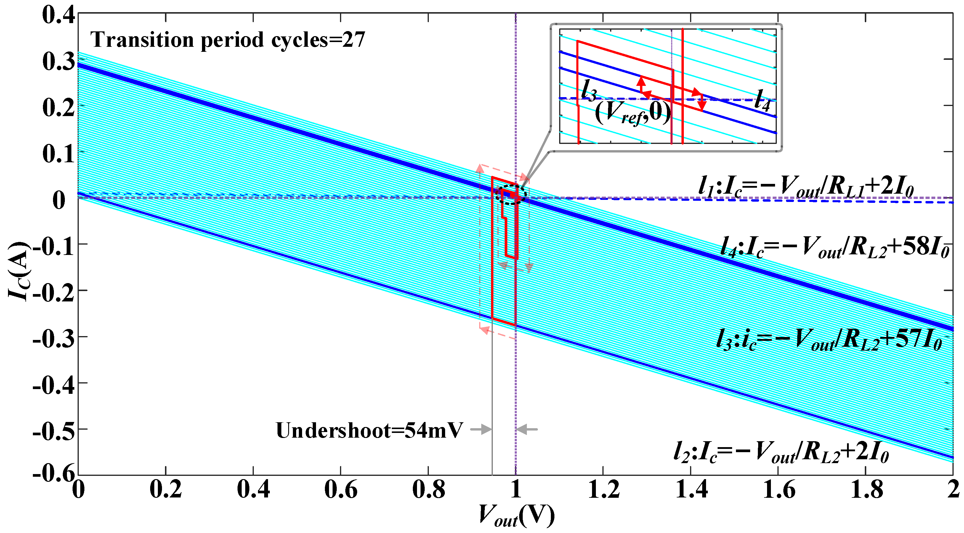
| Overshoot/Reverse Overshoot (mV) | 54 | 88 | 75 | 23 |
| Response time (Tclk) | 27 | 35 | 24 | 16 |
| Literature | This Paper | JSSC, 2018 [13] | JSSC, 2021 [5] | ISSCC, 2020 [9] | ISSCC, 2019 [15] |
|---|---|---|---|---|---|
| Process | 180 nm BCD | 65 nm CMOS | 65 nm CMOS | 28 nm CMOS | 65 nm CMOS |
| Area (mm2) | 0.63 | 0.023 | 0.36 | 0.049 | 0.048 |
| Output Capacitance (nF) | 0.1 | 0.4 | 0.25 | 0.00411 | 100 |
| vin (V) | 1.2 | 0.5–1 | 1.2 | 0.5–1 | 0.5–1 |
| vout (V) | 1 | 0.3–0.45 | 0.6–1.15 | 0.45–0.95 | 0.4–0.95 |
| Power (mW) | 1–200 | 0.03–0.9 | <575 | 72–45 | <0.257 |
| Current Peak Efficiency | 99.9% | 99.8% | 99.98% | 99.99% | 99.99% |
| Clock Frequency (MHz) | 1–100 | 1–240 | 100 | 120 | × |
| Load Regulation (mV/mA) | <0.06 | <5.6 | 0.03 | × | <10 |
| Linear Regulation (mV/V) | 1.6 | 2.3 | × | × | × |
| Overshoot/Current step (mV/mA) | 0.51 | 37.7 | 0.122 | 0.26 | 283.3 |
| Transient time/Current step (μs/mA) | 0.113 | 0.014 | 0.00049 | 0.0000033 | 35.2 |
Disclaimer/Publisher’s Note: The statements, opinions and data contained in all publications are solely those of the individual author(s) and contributor(s) and not of MDPI and/or the editor(s). MDPI and/or the editor(s) disclaim responsibility for any injury to people or property resulting from any ideas, methods, instructions or products referred to in the content. |
© 2025 by the authors. Licensee MDPI, Basel, Switzerland. This article is an open access article distributed under the terms and conditions of the Creative Commons Attribution (CC BY) license (https://creativecommons.org/licenses/by/4.0/).
Share and Cite
Wang, Y.; Ke, J.; Min, R.; Xu, H.; Guan, Z.; Zhang, S.; Liu, C.; Feng, J. Initial/Last-State-Correlated SAR Control with Optimized Trajectory to Reduce Reverse Overshoot and Smooth Current Switching of Hybrid LDOs. Electronics 2025, 14, 2051. https://doi.org/10.3390/electronics14102051
Wang Y, Ke J, Min R, Xu H, Guan Z, Zhang S, Liu C, Feng J. Initial/Last-State-Correlated SAR Control with Optimized Trajectory to Reduce Reverse Overshoot and Smooth Current Switching of Hybrid LDOs. Electronics. 2025; 14(10):2051. https://doi.org/10.3390/electronics14102051
Chicago/Turabian StyleWang, Yinyu, Jinkun Ke, Run Min, Hangyu Xu, Zhaoliang Guan, Shuo Zhang, Chang Liu, and Jingbo Feng. 2025. "Initial/Last-State-Correlated SAR Control with Optimized Trajectory to Reduce Reverse Overshoot and Smooth Current Switching of Hybrid LDOs" Electronics 14, no. 10: 2051. https://doi.org/10.3390/electronics14102051
APA StyleWang, Y., Ke, J., Min, R., Xu, H., Guan, Z., Zhang, S., Liu, C., & Feng, J. (2025). Initial/Last-State-Correlated SAR Control with Optimized Trajectory to Reduce Reverse Overshoot and Smooth Current Switching of Hybrid LDOs. Electronics, 14(10), 2051. https://doi.org/10.3390/electronics14102051