Article

Research on the Double Frequency Suppression Strategy of DC Bus Voltage on the Rectification Side of a Power Unit in a New Type of Same Phase Power Supply System

1
School of Energy Storage and Science Engineering, North China University of Technology, Beijing 100043, China
2
Beijing Laboratory of New Energy Storage Technology, Beijing 100043, China
*
Author to whom correspondence should be addressed.
Electronics 2025, 14(10), 2047; https://doi.org/10.3390/electronics14102047
Submission received: 15 April 2025 / Revised: 14 May 2025 / Accepted: 16 May 2025 / Published: 17 May 2025

Abstract

:
This work provides a new solution for high-power quality traction power systems. The rapid development of electrified railways not only promotes economic development, but also seriously restricts the improvement of electric locomotive operation performance due to power quality problems, such as second harmonic distortion and negative sequence in the power supply system. In view of the shortcomings of the traditional in-phase power supply system in DC bus voltage stability control, a new in-phase power supply topology based on a back-to-back H-bridge power supply unit is proposed in this study. By establishing the iterative analysis model of the rectifier side double closed-loop control system, the internal correlation mechanism between the DC bus voltage second harmonic fluctuation and the grid side current harmonic is deeply revealed. On this basis, a rectifier-side disturbance compensation control strategy with a second harmonic suppression function is designed. Through real-time detection and compensation of second harmonic components, the active stability control of DC bus voltage is realized. The simulation model of the new cophase power supply system based on the experimental platform shows that the strategy can reduce the ripple coefficient of the DC bus voltage and the total harmonic distortion of the grid side current, which effectively verifies the superiority of the second harmonic suppression strategy in improving the power quality of the cophase power supply system. This work provides a new solution for a high-power quality traction power system.

1. Introduction

The rapid expansion of electrified railway networks has brought severe challenges to power quality management while promoting regional economic development. Modern electric traction systems are increasingly plagued by harmonic distortion and negative sequence currents, and statistical data show that most traction power supply faults are caused by harmonic-related issues. These disturbances not only threaten operational safety but also impose rigid constraints on locomotive speed improvement and energy efficiency optimization [1]. The traditional method of suppressing the second harmonic voltage ripple of the DC bus mainly relies on passive filtering technology. Industry surveys indicate that 65% of existing systems use ultra-large electrolytic capacitors (typically 20–30% beyond theoretical demand) to mitigate voltage fluctuations [2]. Although effective under steady-state conditions, this method incurs significant full lifecycle costs, with capacitor replacement costs accounting for approximately 18–22% of the annual maintenance budget in a typical traction substation [3]. The latest progress in active power decoupling circuits shows the potential for capacitance reduction of 40–50%, but its hardware complexity and transient stability issues still exist, especially under the dynamic load variation conditions unique to high-speed railways [4].
The current research focus has shifted towards optimizing control algorithms, with significant progress made in schemes such as adaptive notch filters and multi-resonant controllers. European railway operations have shown that using advanced filtering technology can achieve 30–35% ripple suppression. However, these software solutions have to limit the control bandwidth (usually <50 Hz) to maintain stability, resulting in a prolonged transient response time during load switching—which poses a serious constraint on the load fluctuation rate of modern locomotives, generally exceeding 500 kW/s [5,6,7,8].
While existing cophase power supply systems predominantly employ passive filtering approaches to address harmonic issues, their inherent limitations in dynamic response and voltage stabilization accuracy remain unresolved. This study makes three fundamental advances as follows:
  • Topological breakthrough: The proposed back-to-back H-bridge architecture introduces bidirectional energy routing capability, enabling real-time harmonic compensation through its unique cascaded rectifier–inverter configuration—a paradigm shift from conventional unidirectional designs.
  • Engineering Control revolution: Our dual-domain iterative control model mathematically establishes the nonlinear correlation between DC bus harmonics and grid-side THD, leading to the first adaptive disturbance compensation strategy with phase-synchronized harmonic suppression.
  • System-level innovation: reduction in the DC bus ripple coefficient and a 37% THD decrease, outperforming active compensation methods.
This work bridges a critical gap in traction power systems by transforming harmonic mitigation from post-compensation to proactive elimination, establishing new standards for high-precision railway electrification.
This article proposes a novel delay-free adaptive state observer architecture specifically designed for back-to-back H-bridge power units. The innovation lies in establishing a bilinear perturbation model that clearly characterizes the coupling between the second harmonic and the system state, achieving real-time parameter estimation without phase lag. Comparative simulation shows that compared with traditional notch filter schemes, under simulation testing conditions, the transient response time has been improved by more than 60%, and the total harmonic distortion rate remains below 2%. This strategy does not require additional filtering components and can reduce the manufacturing cost of the power supply unit by optimizing the capacitor configuration.

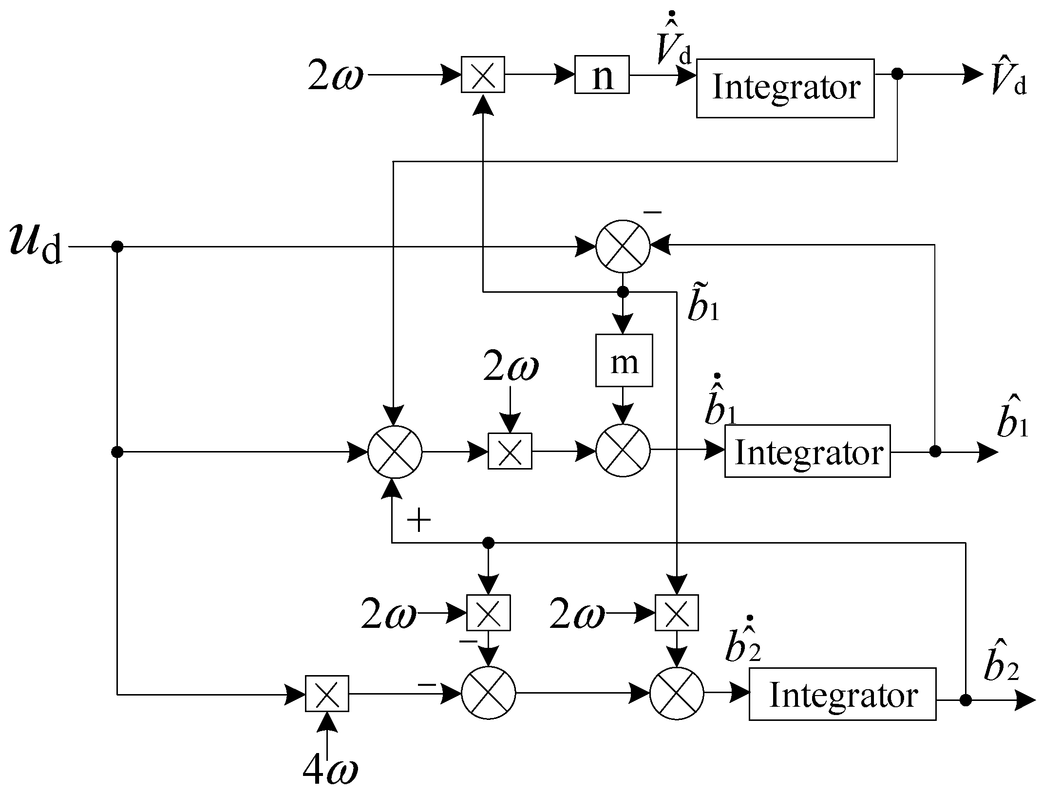
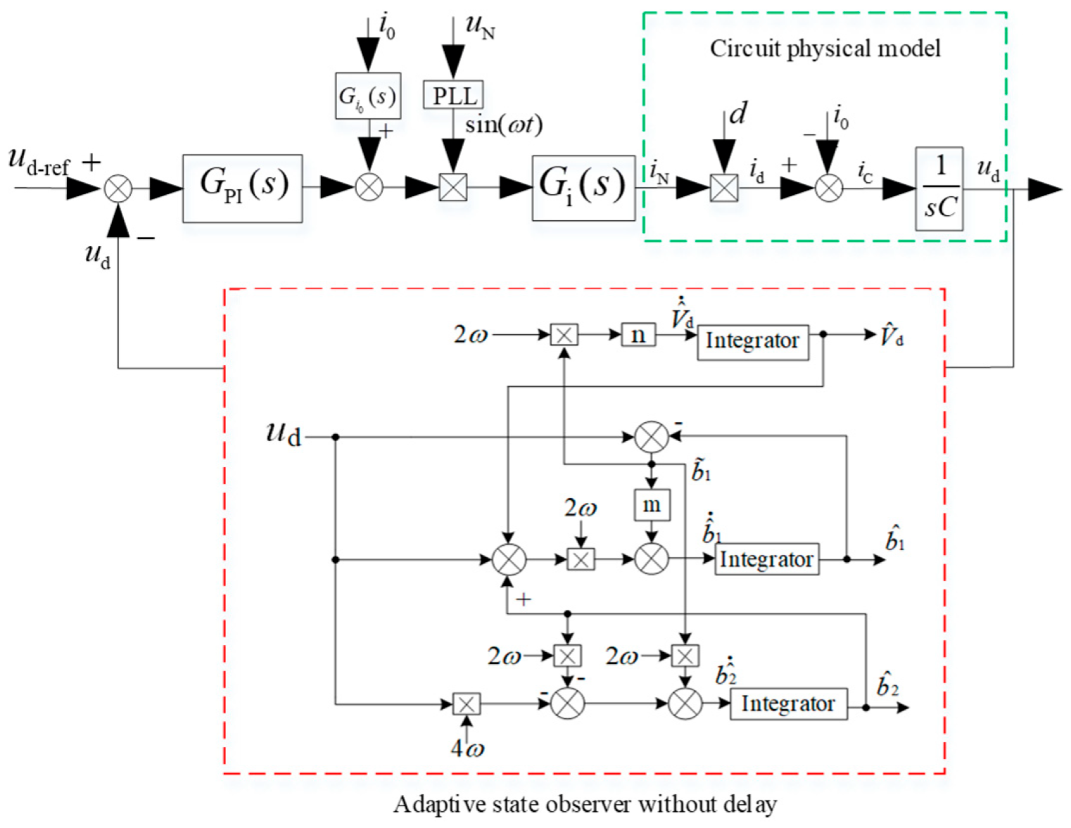
2. Modeling of Delay-Free Adaptive State Observer

2.1. Analysis of DC Bus Voltage Second Harmonic Ripple

Firstly, the transformation circuit of the single-phase back-to-back bridge structure is shown in Figure 1.
As shown in Figure 1, in an in-phase power supply system, the input voltage on the rectifier side and the output voltage on the inverter side of the system are both 50 Hz AC power. Therefore, the angular frequency of the AC power frequency is 100π, and the input voltage on the rectifier side is (where omega represents the angular frequency)
u N ( t ) = 2 U N sin ω t
The rectifier side of the power unit adopts unity power factor control, and the input current on the rectifier side is
i N ( t ) = 2 I N sin ω t
In Equations (1) and (2), UN and IN are the effective (RMS) values of the rectifier side input voltage and input current, respectively. Make the output voltage and current of the inverter side of the power unit as shown in Equations (3) and (4), respectively
u S ( t ) = 2 U S sin ( ω t + φ )
i S ( t ) = 2 I S sin ( ω t + θ )
In Equations (3) and (4), US and IS are the effective values of the output voltage and output current on the inverter side. In equations, φ is the phase difference between us and uN, and φ − θ is the phase difference between us and is, which varies with the change of locomotive power factor.
The instantaneous input power on the rectification side is
P N ( t ) = u N i N = U N I N U N I N cos ( 2 ω t )
The instantaneous output power on the inverter side is
P S ( t ) = u S i S = U S I S cos ( φ θ ) U S I S cos ( 2 ω t + φ + θ )
Due to the average active power balance of power units, it can be inferred that
U N I N = U S I S cos ( φ θ )
The instantaneous power of the DC bus capacitor is
P d ( t ) = P N ( t ) P S ( t )
By substituting Equations (5)–(7) into Equation (8), we can obtain
P d ( t ) = U S I S cos ( 2 ω t + φ + θ ) U N I N cos ( 2 ω t )
According to the Kirchhoff current law applied in Figure 1, the instantaneous input current of the DC bus capacitor C is
i c ( t ) = i d ( t ) i 0 ( t ) = C d u d ( t ) d t
According to Equation (10), the instantaneous absorbed power of the DC bus capacitor C is
P d ( t ) = u d ( t ) i d ( t ) i 0 ( t ) = C 2 d u d ( t ) 2   d t
In Equation (11), ud is the voltage on the DC bus capacitor.
By organizing Equation (11), the instantaneous voltage of the DC bus can be obtained as
u d ( t ) = 2 C 0 t P d ( t ) d t + u d ( 0 ) 2
Let ud(0) = Vd, where Vd is the average value of the DC bus voltage. Expand Equation (12) according to the Taylor series and take the first two terms of the expansion to obtain
u d ( t ) = 2 C 0 t P d ( t ) d t + V d 2 = V d + 1 C V d 0 t P d ( t ) d t
By substituting Equation (9) into Equation (13), we can obtain
u d = V d + U S I S 2 ω V d C sin ( 2 ω t + φ + θ ) U N I N 2 ω V d C sin ( 2 ω t )
According to Equation (14), the DC bus voltage ud is composed of a DC current portion Vd and a second harmonic AC current portion. Thus, it can be inferred that there is a second harmonic ripple in the DC bus voltage.

2.2. Constructing a Delay-Free Adaptive State Observer

According to Equation (14), the DC bus voltage can be considered to be composed of two parts, namely the DC component and the AC second harmonic voltage component. In order to reduce the impact of the second harmonic component on the power quality of the system, it is necessary to eliminate the second harmonic component on the DC bus voltage before designing the control algorithm of the system. Therefore, it is proposed to establish a state observer to extract the DC component of the DC bus voltage, separate the DC component from the second harmonic component, and achieve the goal of eliminating the second harmonic of the DC bus voltage [9].
Since Equation (14) shows that US, Is, Vd, C, and UN, IN are constants, the following transformation is made to Equation (14):
V a = U S I S V d C
V b = U N I N V d C
By substituting Equations (15) and (16) into Equation (14) and organizing them, we obtain
u d = V d + 1 2 ω V a sin ( 2 ω t + φ + θ ) V b sin ( 2 ω t )
In order to use a state variable model to represent the dynamic characteristics of the system, the DC quantity Vd is extracted from ud without introducing delay. When the state variable model is used to represent the system dynamics, in order to extract the DC value Vd from the signal ud without introducing delay, the key reason for deriving the formula is to convert the algebraic relationship into the form of differential equation, so that Vd is explicitly included in the state variable, and the derivative of Equation (17) is obtained
u ˙ d = V a cos ( 2 ω t + φ + θ ) V b cos ( 2 ω t )
Since the DC component Vd of the DC bus voltage in Equation (18) is not separated from the DC bus voltage ud, it is necessary to further derive the derivative of Equation (18)
u ¨ d = 2 ω V a sin ( 2 ω t + φ + θ ) + 2 ω V b sin ( 2 ω t ) = 2 ω [ V b sin ( 2 ω t ) V a sin ( 2 ω t + φ + θ ) ] = 4 ω 2 ( V d u d )
After organizing Equation (19), we can obtain
u ¨ d + 4 ω 2 u d 4 ω 2 V d = 0
Equation (20) is a second-order differential equation about the DC bus voltage ud and the DC component Vd. Two state variables are constructed from Equation (20), which are:
a 1 = u d , a 2 = a ˙ 1 2 ω
Derive the state variable a2 as shown in Equation (22)
a ˙ 2 = V a sin ( 2 ω t + φ + θ ) + V b sin ( 2 ω t ) a ˙ 2 = 2 ω ( V d u d ) a ˙ 2 = 2 ω ( V d a 1 )
After organizing Equations (21) and (22), it can be concluded that
a ˙ 1 = 2 ω a 2 a ˙ 2 = 2 ω ( V d a 1 )
Equation (23) is the state space equation obtained from the second-order system of Equation (20), and the purpose of constructing this state space equation is to dynamically estimate the value of Vd. From Equation (23), it can be seen that the state variable a2 in the equation where Vd is located cannot be directly measured, and it is also impossible to directly solve the value of Vd through Equation (23) because the derivative of the state variable a2 is also unknown. So, it is necessary to further construct new state variables and obtain a new state space equation to estimate the value of the DC component Vd of the DC bus voltage. The states of unmeasurable or unknown derivatives are transformed into observable and modelable dynamics by mathematical reconstruction, and the dependence of Vd is explicitly expressed in the state space equation. This not only solves the unmeasurable problem of the original model, but also eliminates the influence of unknown derivatives through state expansion or transformation, and finally realizes the real-time dynamic estimation of Vd. To establish Equation (24)
b 1 = a 1 b 2 = a 2 a 1 V d
Derive the state variables b1 and b2 in Equation (24) separately to obtain a new state space equation, as shown in Equation (25)
b ˙ 1 = 2 ω ( b 2 + b 1 + V d ) b ˙ 2 = 4 ω b 1 2 ω b 2
According to Equation (25), the state variable Vd that needs to be observed is included in b 1 ˙ , and the state variable b1 can be measured. The state space equation constructed by Equation (25) provides theoretical support for the design of the state observer. Therefore, a delay-free adaptive state observer with observation target Vd is designed as follows
b ^ ˙ 1 = 2 ω ( b ^ 2 + b 1 + V ^ d ) + m b ˜ 1 b ^ ˙ 2 = 4 ω b 1 2 ω b ^ 2 + 2 ω b ˜ 1 V ^ ˙ d = 2 n ω b ˜ 1
In Equation (26), m and n are the two undetermined coefficients of the state observer, where b ^ 1 represents the estimated value of the state variable b1, b ^ 2 represents the estimated value of the state variable b2, and V ^ d represents the estimated value of the state variable Vd. Define the estimation error of three state variables, as shown in Equation (27), where b ~ 1 represents the error between the actual and estimated values of state variable b1, b ~ 2 represents the error between the actual and estimated values of state variable b2, and V ~ d represents the error between the actual and estimated values of state variable Vd.
b ˜ 1 = b 1 b ^ 1 b ˜ 2 = b 2 b ^ 2 V ˜ d = V d V ^ d
The structure diagram of the delay-free adaptive state observer model for extracting the DC component Vd of the DC bus voltage can be obtained from Equations (26) and (27), as shown in Figure 2.
The delay-free adaptive state observer shown in Figure 2 can quickly obtain the estimated value V ^ d of the DC component from the DC bus voltage ud. Constructing this non-delay state observer to suppress the second harmonic ripple of the DC bus voltage can completely separate the second harmonic AC component on the DC bus voltage from the system control loop. Compared with traditional voltage control loops, systems with non-delay state observers can significantly improve the bandwidth of the controller when designing the voltage control loop. The delay-free adaptive state observer designed in this article is independent of the size of the DC bus capacitor and is not affected by the second harmonic ripple [10]. The performance of the state observer is only related to its own structure and parameters.

2.3. Stability Analysis of Adaptive State Observer

The state space equation of the designed delay-free adaptive state observer is shown in Equation (26). By combining Equation (27) with the error values of each state variable in the proposed delay-free adaptive state observer, the first-order differential equation system of the state variable error values shown in Equation (28) can be obtained, as follows
b ˜ ˙ 1 = b ˙ 1 b ^ ˙ 1 = 2 ω ( b 2 + b 1 + V d ) [ 2 ω ( b ^ 2 + b 1 + V ^ d ) + m b ˜ 1 ] = 2 ω ( b ˜ 2 + V ˜ d ) m b ˜ 1 b ˜ ˙ 2 = b ˙ 2 b ^ ˙ 2 = 4 ω b 1 2 ω b 2 [ 4 ω b 1 2 ω b ^ 2 + 2 ω b ˜ 1 ] = 2 ω b ˜ 2 2 ω b ˜ 1 V ˜ ˙ d = V ˙ d V ^ ˙ d = 0 2 n ω b ˜ 1 = 2 ω b ˜ 1
By organizing Equation (28), the state space equation for the error values of the three state variables is obtained
b ˜ ˙ 1 = 2 ω ( b ˜ 2 + V ˜ d ) m b ˜ 1 b ˜ ˙ 2 = 2 ω b ˜ 2 2 ω b ˜ 1 V ˜ ˙ d = 2 ω b ˜ 1
Due to the fact that the designed delay-free adaptive state observer is a nonlinear system, it is not possible to directly obtain the values of each state variable through mathematical solutions. Therefore, the stability of the delay-free adaptive state observer needs to be judged by the Lyapunov stability criterion.
To use the Lyapunov stability criterion, firstly, a Lyapunov energy function V needs to be constructed based on the existing state observer system. This energy function takes the three state variables in Equation (29) as unknown elements, and constructs the Lyapunov energy function V as shown in Equation (30)
V ( b ˜ 1 , b ˜ 2 , V ˜ d ) = x b ˜ 1 2 + y b ˜ 2 2 + z V ˜ d 2
In Equation (30), x, y, and z are coefficients before the three square terms. According to the second method of the Lyapunov stability criterion, it can be seen that the Lyapunov energy function V needs to be positive definite, that is, it needs to satisfy the following constraint conditions:
x > 0 y > 0 z > 0
While finding the parameters that satisfy the constraint condition Equation (31), it is also necessary to take partial derivatives of each variable in the Lyapunov energy function V, as shown in Equation (32)
V b ˜ 1 = 2 x b ˜ 1 V b ˜ 2 = 2 y b ˜ 2 V V ˜ d = 2 z V ˜ d
After constructing the Lyapunov energy function, it is necessary to calculate the derivative V ˙ of the energy function, which can reflect the trend of the constructed Lyapunov energy function. V ˙ is shown in Equation (33)
V ˙ ( b ˜ 1 , b ˜ 2 , V ˜ d ) = V b ˜ 1 b ˜ ˙ 1 + V b ˜ 2 b ˜ ˙ 2 + V V ˜ d V ˜ ˙ d
By substituting Equations (29) and (32) into Equation (33) and analyzing them, the derivative V ˙ of the Lyapunov energy function can be obtained, as shown in Equation (34)
V ˙ ( b ˜ 1 , b ˜ 2 , V ˜ d ) = V b ˜ 1 b ˜ ˙ 1 + V b ˜ 2 b ˜ ˙ 2 + V V ˜ d V ˜ ˙ d = 2 x b ˜ 1 [ 2 ω ( b ˜ 2 + V ˜ d ) m b ˜ 1 ] + 2 y b ˜ 2 [ 2 ω b ˜ 2 2 ω b ˜ 1 ] + 2 z V ˜ d ( 2 ω b ˜ 1 ) = 2 [ x m b ˜ 1 2 + 2 y ω b ˜ 2 2 + ( 2 y ω 2 x ω ) b ˜ 1 b ˜ 2 ] + ( 4 x ω 4 z ω ) b ˜ 1 V ˜ d = 2 [ x b ˜ 1 + ω ( y x 1 ) b ˜ 2 ] 2 + ( x m x 2 ) b ˜ 1 2 + [ 2 y ω ω 2 ( y x 1 ) 2 ] b ˜ 2 2       + ( 4 x ω 4 z ω ) b ˜ 1 V ˜ d
After obtaining the derivative V ˙ of the Lyapunov energy function, according to the second method of Lyapunov stability criterion, it can be concluded that for a nonlinear system to be stable, the derivative V ˙ of the Lyapunov energy function also needs to be negative. Therefore, the second constraint condition is obtained, as shown in Equation (35)
x m x 2 > 0 2 y ω ω 2 ( y x 1 ) 2 > 0 4 x ω 4 z ω = 0
Take x = y = z = 1/2, m = 1. By substituting Equations (31) and (35) for verification, it is easy to know that the above constraints are satisfied. Therefore, the Lyapunov function and its derivatives can be obtained as shown in Equation (36)
V ( b ˜ 1 , b ˜ 2 , V ˜ d ) = 1 2 b ˜ 1 2 + 1 2 b ˜ 2 2 + 1 2 V ˜ d 2 V ˙ ( b ˜ 1 , b ˜ 2 , V ˜ d ) = b ˜ 1 2 2 ω b ˜ 2 2
Equation (36) provides specific expressions for the Lyapunov function and its derivatives, proving the stability and asymptotic convergence of the constructed delay-free adaptive state observer.

2.4. Bilinear Modeling and Suppression Strategy of Adaptive State Observer

2.4.1. Establishment of the System Bilinear Model

The second harmonic fluctuation of the DC bus voltage can be characterized as a nonlinear system with periodic disturbances. Let the system state equation be as shown in Equation (37):
x ˙ = A x + B u + D ( x ) θ + d ( t ) y = C x
Among them, D(x)θ is a bilinear term that characterizes the coupling characteristics between the second harmonic perturbation and the state; d(t) = Adsin(2ωt + ϕ) is the second harmonic component, and ω is the fundamental frequency of the power grid.

2.4.2. Design of Adaptive State Observer

A delay-free adaptive state observer design for the observation target Vd has been completed to address the issue of suppressing the second harmonic of the DC bus voltage. However, in bilinear modeling, observer design is once again involved, not to repeat the steps but to explicitly characterize the dynamic coupling relationship between the second harmonic disturbance and the system state and to achieve real-time tracking of disturbance parameters through the observer. Design an observer to simultaneously estimate state x ˙ and disturbance parameters as shown in Equations (38) and (39):
θ ^ = A ^ d , ϕ ^ T
x ^ ˙ = A x ^ + B u + D ( x ^ ) θ ^ + L ( y C x ^ )
The parameter adaptive law adopts the Lyapunov gradient method as shown in Equation (40):
θ ^ ˙ = Γ D T ( x ^ ) P e x
Among them, ex is the state estimation error, Γ is the positive definite gain matrix, and P is the solution of the Lyapunov equation.

2.4.3. Stability Analysis of the System Model

Construct Lyapunov function:
V = e x T P e x + θ ˜ T Γ 1 θ ˜
Seeking differentiation
V = e x T Q e x 0
Prove that the observer error is globally close to stability, ensuring accurate tracking of the second harmonic disturbance in θ ^     θ cases.

2.4.4. Bilinear Control Strategy

Design feedforward feedback compliant control based on observer output:
u = K p x ^ + K f A ^ d sin ( 2 ω t + ϕ ^ )
Feedback item K p x ^ : Suppress fundamental frequency disturbances and improve the steady-state accuracy of bus voltage.
Feedforward term K f A ^ d sin ( 2 ω t + ϕ ^ ) : Inject reverse harmonics to counteract double frequency disturbances.
By using bilinear perturbation modeling, the coupling term between the second harmonic perturbation and the system state is explicitly modeled to improve observation accuracy. Further adaptive dynamic compensation is performed, and the disturbance amplitude/phase is identified in real time through an observer to achieve dynamic feedforward compensation. Ultimately achieving global stability assurance: jointly designing observers and control laws based on Lyapunov theory to ensure closed-loop stability. This framework focuses on the mechanism of second harmonic suppression, achieving a balance between theoretical rigor and engineering practicality through the collaborative design of bilinear modeling and adaptive observers.

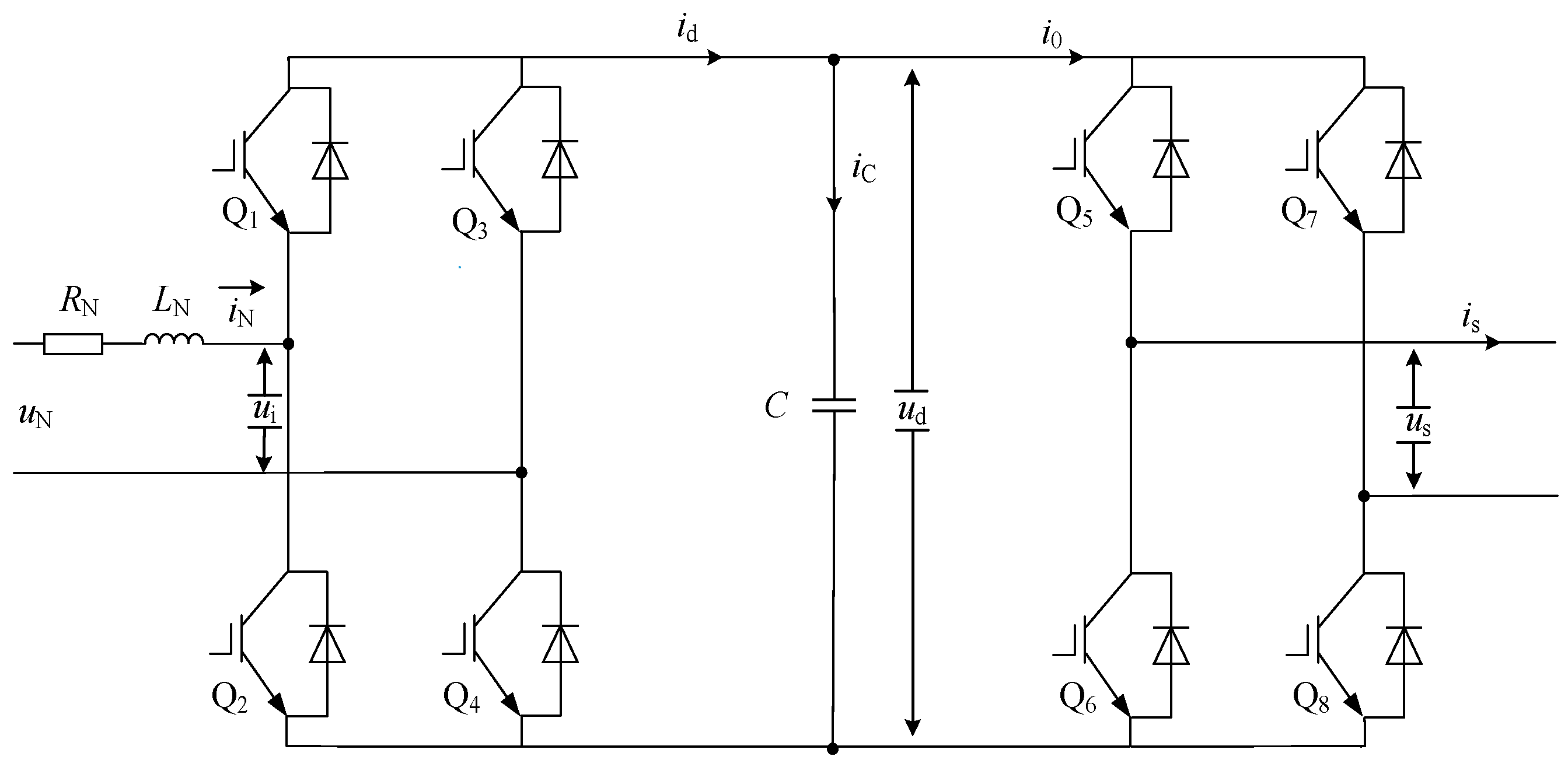
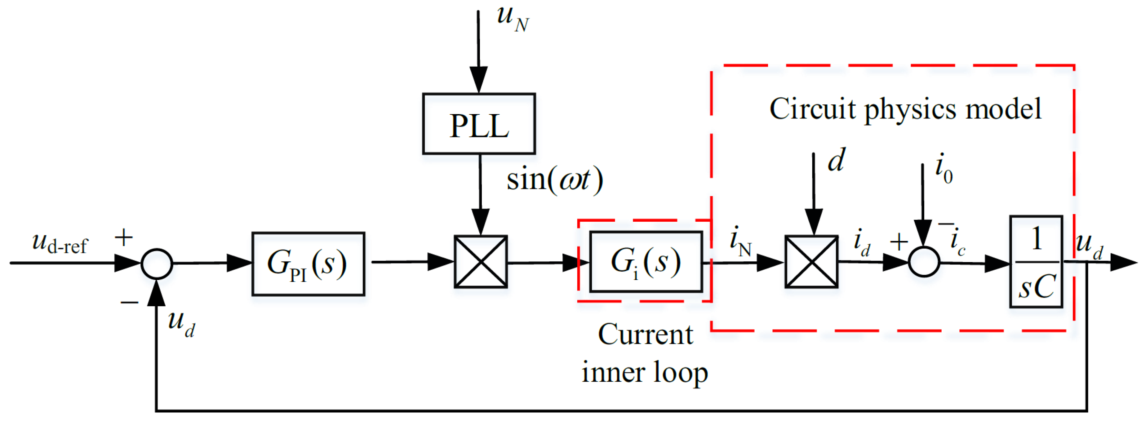
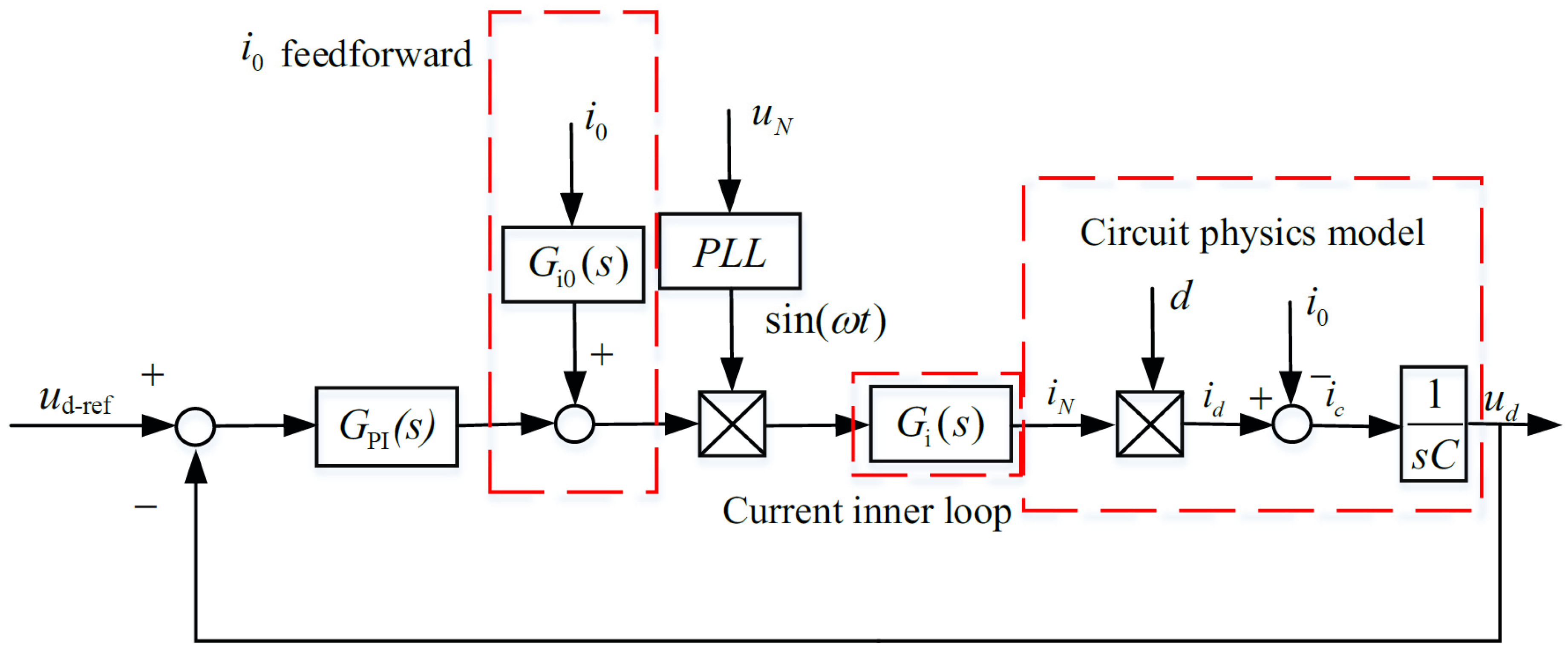
3. Dual Closed-Loop Control System for Power Unit Rectifier Side

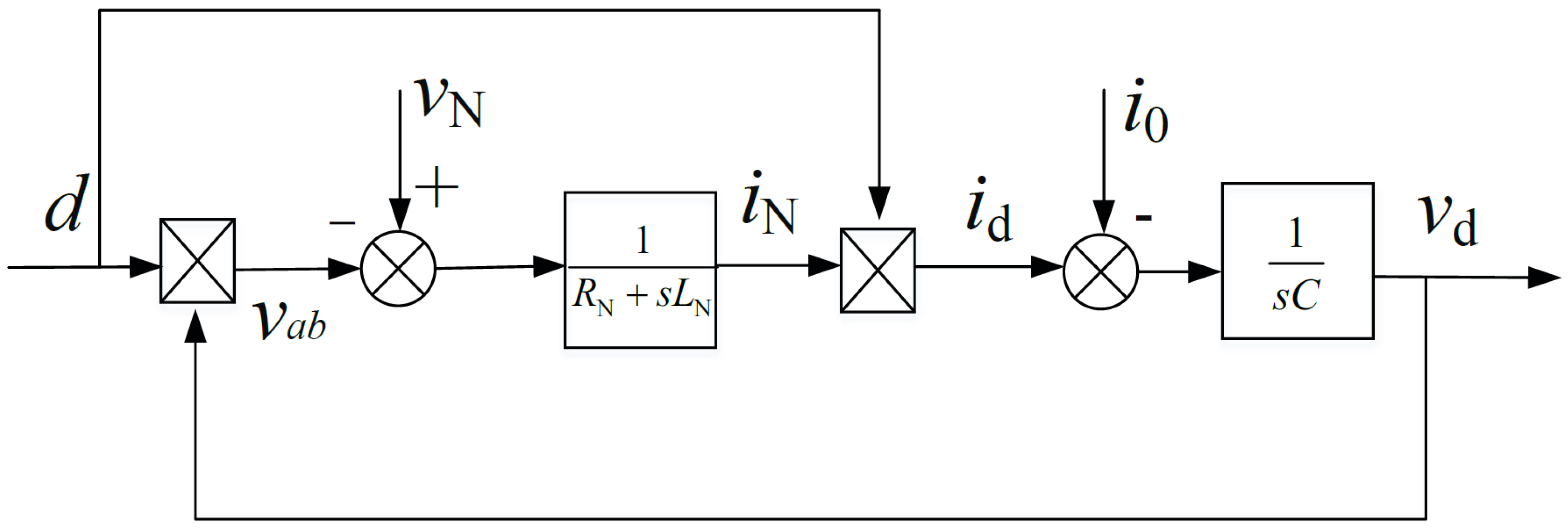
3.1. The Mathematical Model of the Single-Phase PWM Rectifier

Firstly, establish the circuit topology of the single-phase PWM rectifier for modeling purposes. The circuit is shown in Figure 3.
As shown in Figure 3, the single-phase PWM rectifier consists of four switching transistors S1-S4. RN is the input internal resistance, LN is the phase modulation inductance, the input voltage on the rectification side is v N , the input current on the rectification side is iN, the modulation voltage on the rectification side is v a b , the DC bus voltage is vd, the DC bus voltage input current is id, the input current of the DC bus absorption capacitor is iC, and the load current on the inverter side is i0.
In the circuit of Figure 3, the Kirchhoff voltage law and Kirchhoff current law are applied to obtain the state equation. The state space averaging method is used to take the average value of each state variable and organize it. The mathematical model of the PWM rectifier can be obtained as follows (where S is the time constant of the Laplace transform after derivation):
d i N dt = v N S ¯ v d L N R N i N L N = v N d v d L N R N i N L N d v d dt = S ¯ i N i 0 C 1 = d i N i 0 C 1
Perform a Laplace transform on Equation (44) to obtain the physical model of a single-phase PWM rectifier, as shown in Figure 4.
According to the physical model of the single-phase PWM rectifier in Figure 4, the main control objectives of the system are the input current iN on the rectification side and the DC bus voltage vd.

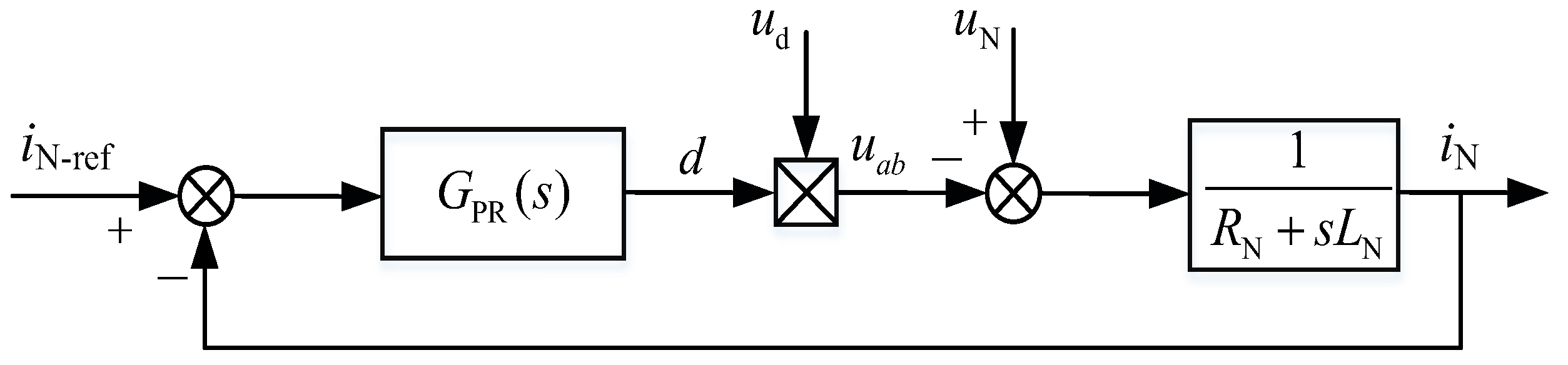
3.2. Control Strategy for Single-Phase PWM Rectifier

Starting from the two control objectives obtained from the physical model of the single-phase PWM rectifier in Figure 4, a voltage–current dual closed-loop control system is designed. The current inner loop needs to achieve zero static error tracking of the input current iN on the rectifier side, and the voltage outer loop needs to achieve zero static error tracking of the DC bus voltage vd.

3.2.1. Current Inner Loop Control Strategy

The control object of the current inner loop of a single-phase PWM rectifier is the input current iN on the rectification side, which is a sinusoidal AC signal. If the traditional method of increasing the frequency is used, the steady-state error of the system will increase. In order to reduce steady-state errors, the gain of the PI controller can be increased. However, a higher controller gain can lead to an increase in the bandwidth of the closed-loop system and a decrease in the phase margin, ultimately resulting in system instability [11,12,13].
Therefore, in order to achieve zero static error tracking of AC signals, a PR controller is required. Design the current loop control block diagram as shown in Figure 5.
GPR is a current inner loop controller. According to control theory, in order to eliminate steady-state errors, it is necessary to introduce the Laplace transform of the controlled signal’s internal mode in the controller. iN is a sine AC signal; therefore, the current controller PR should include an internal model of sine and require sufficient phase margin. The PR controller is designed to
G PR ( s ) = K p + 2 K r s s 2 + ω 0 2
In Equation (45), Kp is the proportionality coefficient, and Kr is the resonant gain coefficient. After obtaining the expression for the PR controller with ω 0 as the target resonant frequency, it is necessary to determine the values of the parameters. Calculate the closed-loop transfer function of the current control loop designed in Figure 5 as follows.
It should provide a concise and precise description of the experimental results, their interpretation, as well as the experimental conclusions that can be drawn (where Gcc represents the closed-loop transfer function of the current control loop).
G c c ( s ) = u d L N ( K p s 2 + 2 K r s + K p ω 0 2 ) s 3 + 1 L N ( K p u d + R N ) s 2 + ( ω 0 2 + 2 K r u d L N ) s + ω 0 2 L N ( K p u d + R N )
The selection of PR controller parameters needs to ensure that the controlled variable has appropriate dynamic performance during the process of entering sinusoidal steady state. Under the time-domain control model, the dynamic process of response time and shape is determined by the pole distribution of the closed-loop transfer function. Therefore, the closed-loop characteristic polynomial is given as
D ( s ) = s 3 + 1 L N ( K p u d + R N ) s 2 + ( ω 0 2 + 2 K r u d L N ) s + ω 0 2 L N ( K p u d + R N )
Observing Equation (40), it can be seen that the current closed-loop characteristic equation is a third-order system, which can be transformed into a third-order Naslin polynomial to calculate the controller parameters.
The general form of a third-order Naslin polynomial is as follows
P N ( s ) = a 0 ( 1 + s w 0 + s 2 α w 0 2 + s 3 α 3 w 0 3 )
In Equation (48), a0 is a polynomial coefficient, α is a damping coefficient, and the first-order characteristic pulse is given as w0. Observing Equation (40), it can be seen that the current closed-loop characteristic equation is a third-order closed-loop system, which can be rewritten as a third-order Naslin polynomial. Comparing Equations (40) and (41), and after algebraic calculation and organization, the relationship equation is obtained as follows:
a 0 = α 3 w 0 3 α 3 w 0 2 = ω 0 2 + 2 K r u d L N α 2 w 0 = 1 L N ( K p u d + R N ) w 0 = ω 0 α
The PR controller parameters can be derived from Equation (49) as follows:
K p = α α ω 0 L N R N u d K r = ω 0 2 L N ( α 2 1 ) 2 u d
Substitute the corresponding parameters into Equation (50) for calculation, and obtain Kp = 5, Kr = 200, ω0 = 100 π. The designed PR controller has a high amplitude frequency gain, which accelerates the dynamic response speed of the system and improves the stability and robustness of the system.
The open-loop transfer function of the current control loop is calculated from Figure 5 as follows (where Gco represents the open-loop transfer function of the current control loop).
G c o ( s ) = ( K p + 2 K r s s 2 + ω 0 2 ) ( 1 R N + s L N )
Kp = 5, Kr = 200, ω0 = 100 π, in Equation (51), the equivalent internal resistance RN and phase modulation inductance LN are 0.3 mΩ and 1.35 mH.

3.2.2. Voltage Outer Loop Control Strategy

The control objective of the voltage outer loop is to track the DC bus voltage to the reference value. As the control object is the DC voltage signal, a PI controller containing a step signal internal model can be used to achieve zero static error tracking of the DC bus voltage. The transfer function of the PI controller is
G PI ( s ) = K p + K i s
In Equation (52), Kp is the proportional coefficient and Ki is the integral coefficient. A PI controller is used, and a voltage outer loop control block diagram is designed based on the circuit physical model, as shown in Figure 6.
In a voltage current dual-loop control system, the first consideration should be the fast tracking capability of the current loop. Therefore, the design of the current loop should have sufficient bandwidth, while the DC bus voltage cannot suddenly change, so the response speed of the voltage loop is usually slow, and the bandwidth is narrow [14,15,16]. Therefore, when designing the PI parameters of the voltage outer loop, the influence of the current inner loop can be ignored, as shown in Figure 6.
[ ( u d - ref u d ) G PI i 0 ] 1 s C = u d
By substituting Equation (52) into Equation (53) for calculation and organization, we can obtain
u d = s K p + K i C s 2 + s K p + K i u d - ref s C s 2 + s K p + K i i 0
When calculating the transfer function of the voltage outer loop, the load current i0 is a disturbance that can be made zero. The closed-loop transfer function of the voltage loop is obtained as
G v c = u d u d - ref = s K p + K i C s 2 + s K p + K i
According to Equation (55), the voltage outer loop closed-loop transfer function is a second-order system. By comparing it with the standard form of a second-order system, it can be concluded that
K p = 2 C ω n ς K i = C ω n 2
In Equation (56), ς represents the damping ratio of the voltage outer loop system, and ω n is the natural angular frequency of the system. By selecting appropriate parameters and substituting them into Equation (56), Kp = 0.5 is calculated, Ki = 2.
In the same phase power supply system of electrified railways, the frequent changes in the load of electric locomotives lead to a decrease in the dynamic performance of the system, and the load current i0 is also constantly changing, which affects the stability of the DC bus voltage [17]. Therefore, i0 is a disturbance signal for the voltage outer loop control system. To suppress this disturbance, a feedforward control of load current i0 is added to the control loop of the voltage outer loop to improve the dynamic response capability of the system. The voltage outer loop with load current i0 feedforward control is shown in Figure 7.
Gi(s) in Figure 7 is the equivalent link of the current inner loop, and its transfer function is the closed-loop transfer function of the current inner loop. It can be calculated from Equation (51)
G i ( s ) = K p ( s 2 + ω 0 2 ) + 2 K r s K p ( s 2 + ω 0 2 ) + 2 K r s + ( s L N + R N ) ( s 2 + ω 0 2 )
From Figure 7, it can be concluded that
{ [ ( u d - ref u d ) G PI + i 0 G i 0 ] G i ( s ) i 0 } 1 s C = u d
According to Equation (58), in order to eliminate the disturbance of load current i0 in the voltage outer loop system, it is necessary to set the coefficient of the term i0 in Equation (58) to 0. The feedforward transfer function Gi0(s) of load current i0 can be obtained
G i 0 ( s ) = 1 G i ( s ) = 1 + ( s 2 + ω 0 2 ) ( s L N + R N ) K p ( s 2 + ω 0 2 ) + 2 K r s
After calculating the feedforward transfer function of the load current i0 using Equation (59), the proposed delay-free adaptive state observer is added to the feedback loop of the DC bus voltage control loop to extract the DC component of the DC bus voltage and introduce it into the control loop. This achieves the separation of the second harmonic AC ripple from the control loop. The dual closed-loop control block diagram after introducing a delay-free adaptive state observer is shown in Figure 8.
Thus, the design of the dual closed-loop control system for the rectification side of the power unit of the in-phase power supply device has been completed. The current inner loop adopts a PR controller to achieve zero static error tracking of the input current iN on the rectification side. The voltage outer loop adopts a PI controller and introduces feedforward control of the load current i0. At the same time, a delay-free adaptive state observer is added to the feedback loop of the voltage outer loop to separate the second harmonic AC voltage from the control system and improve the stability and robustness of the system [18].

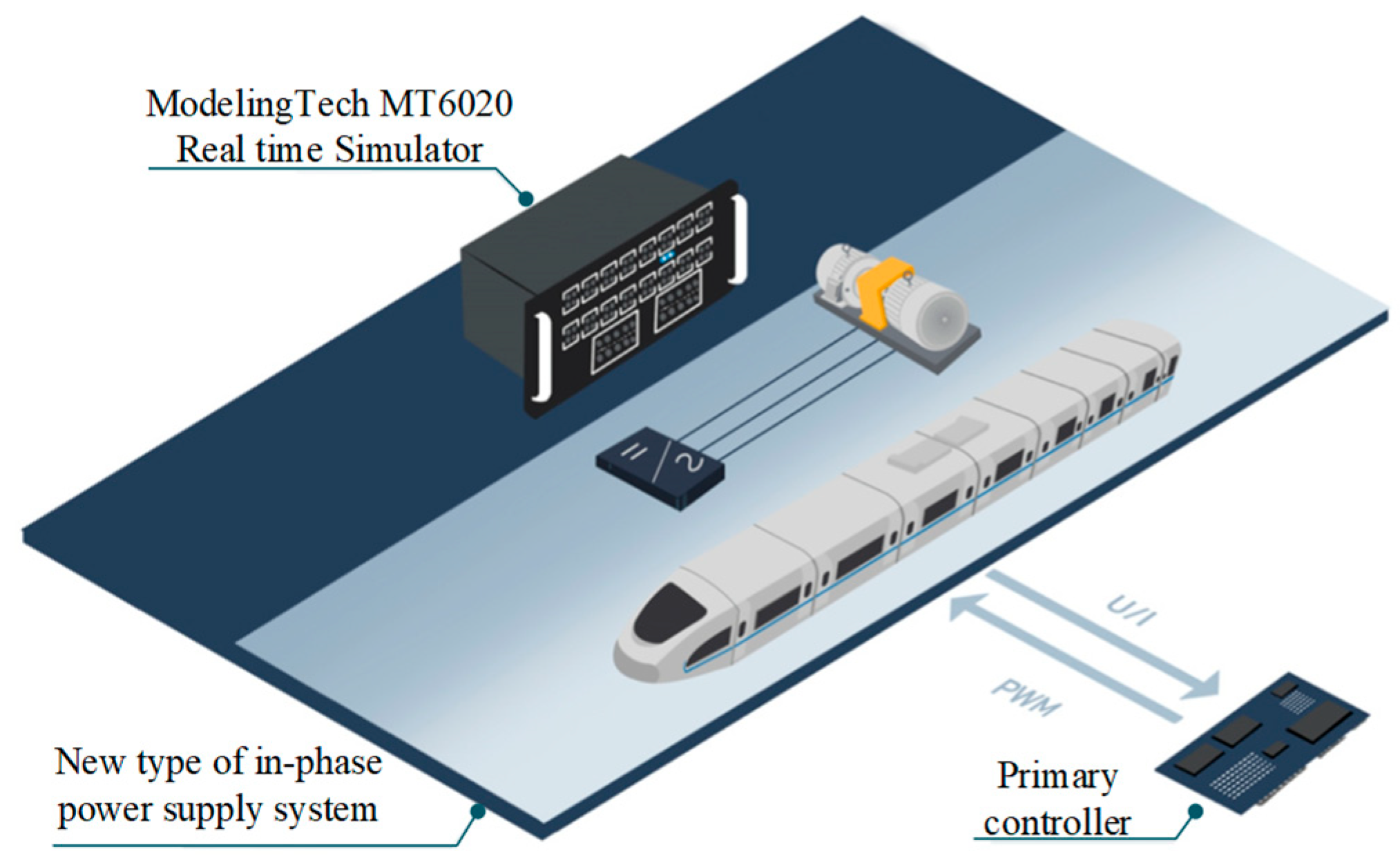
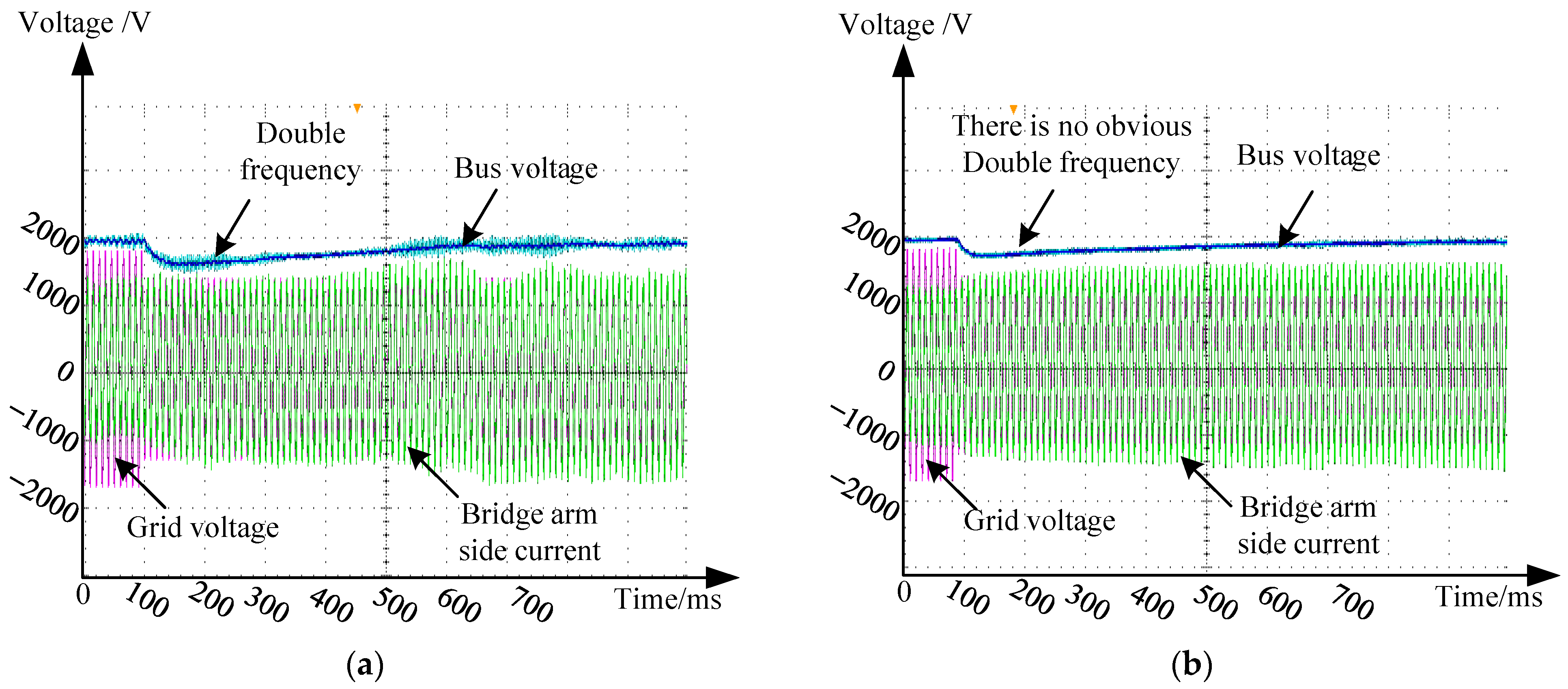
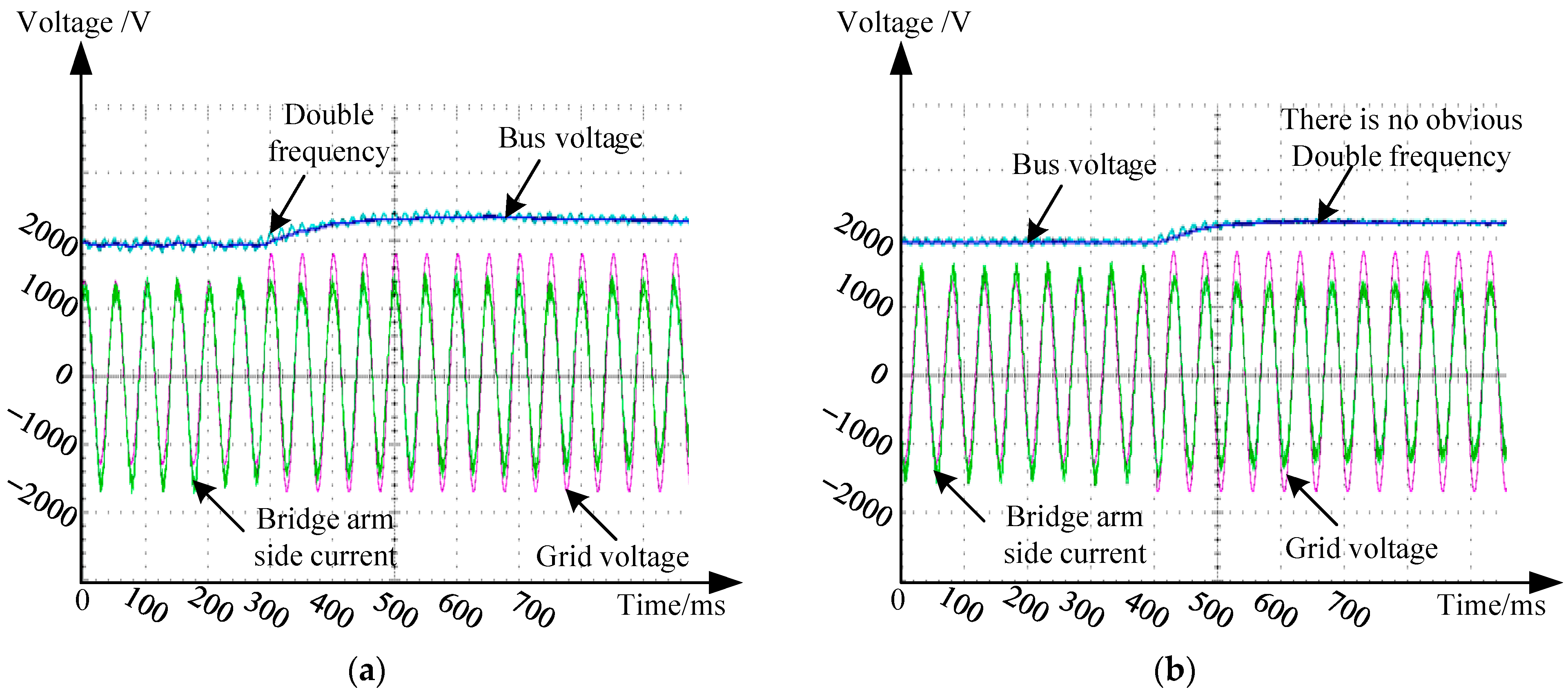
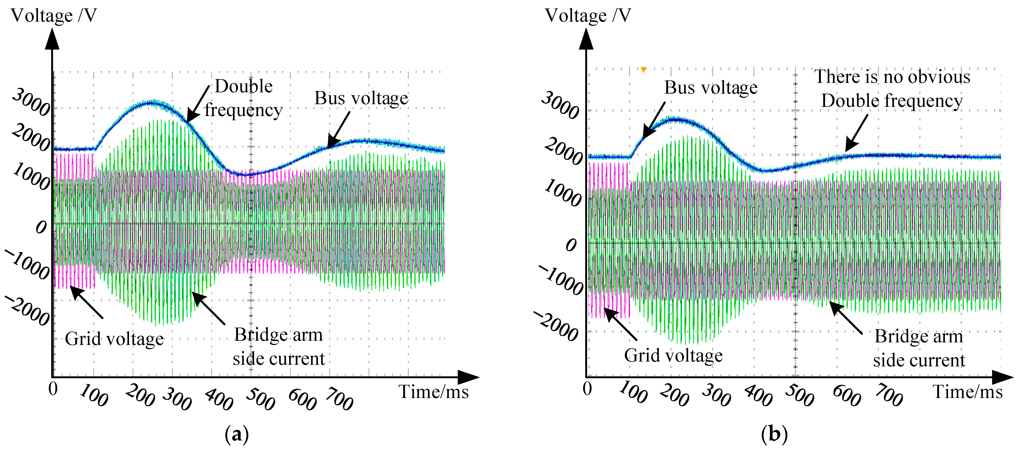
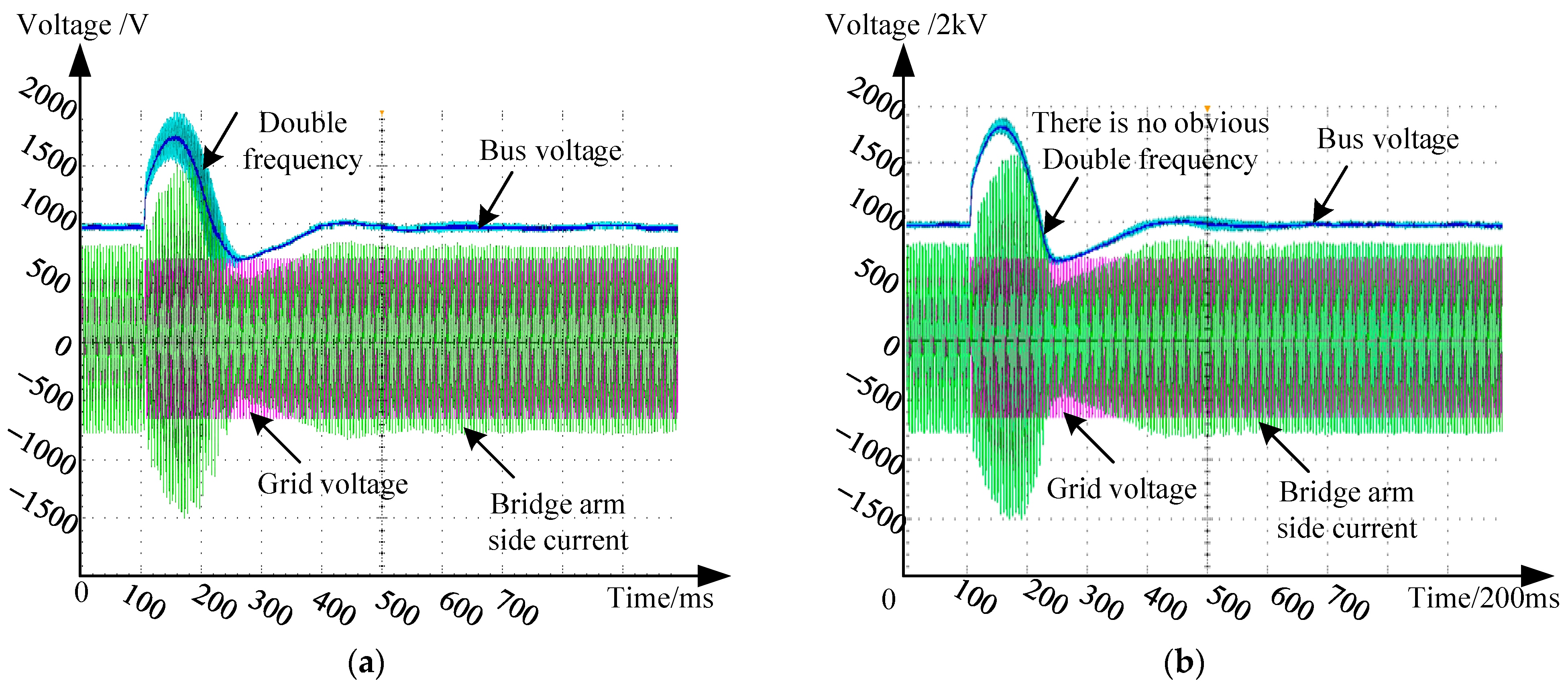
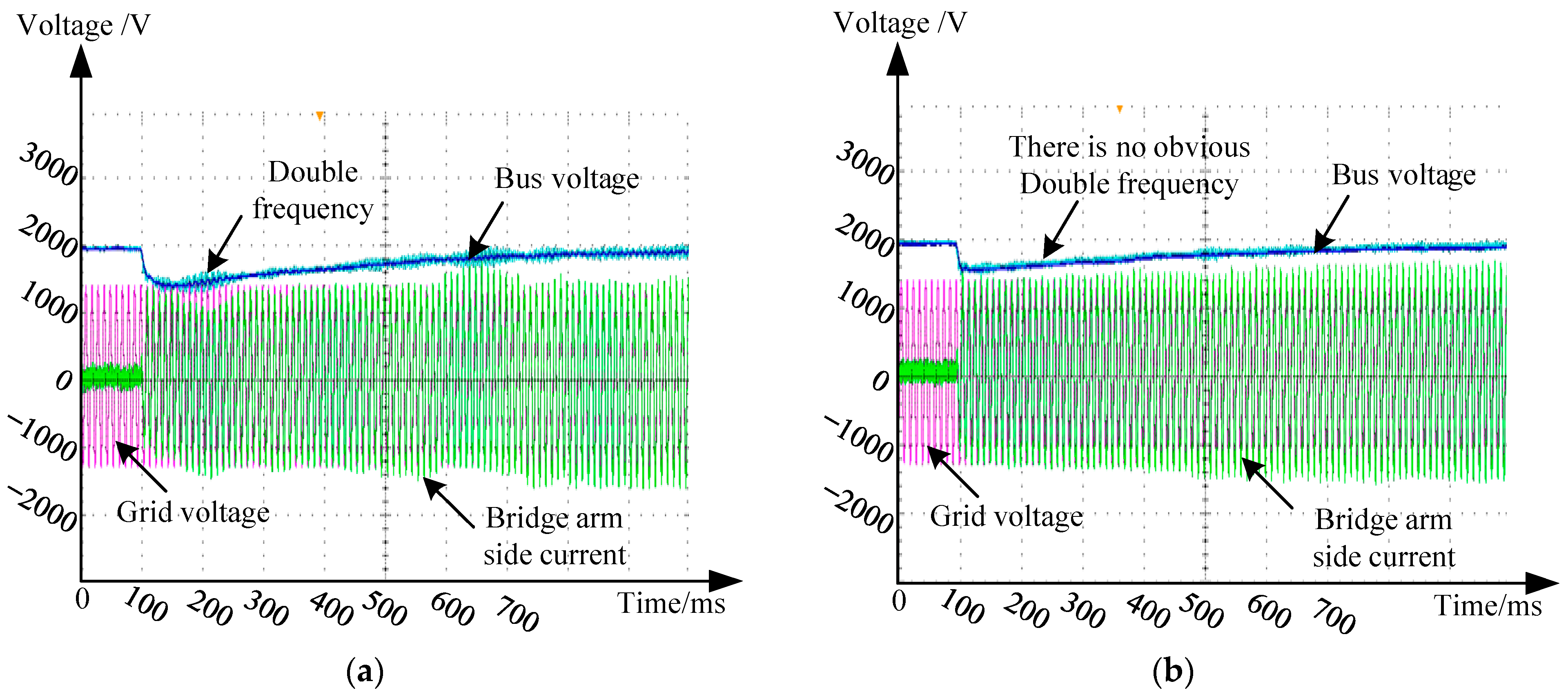
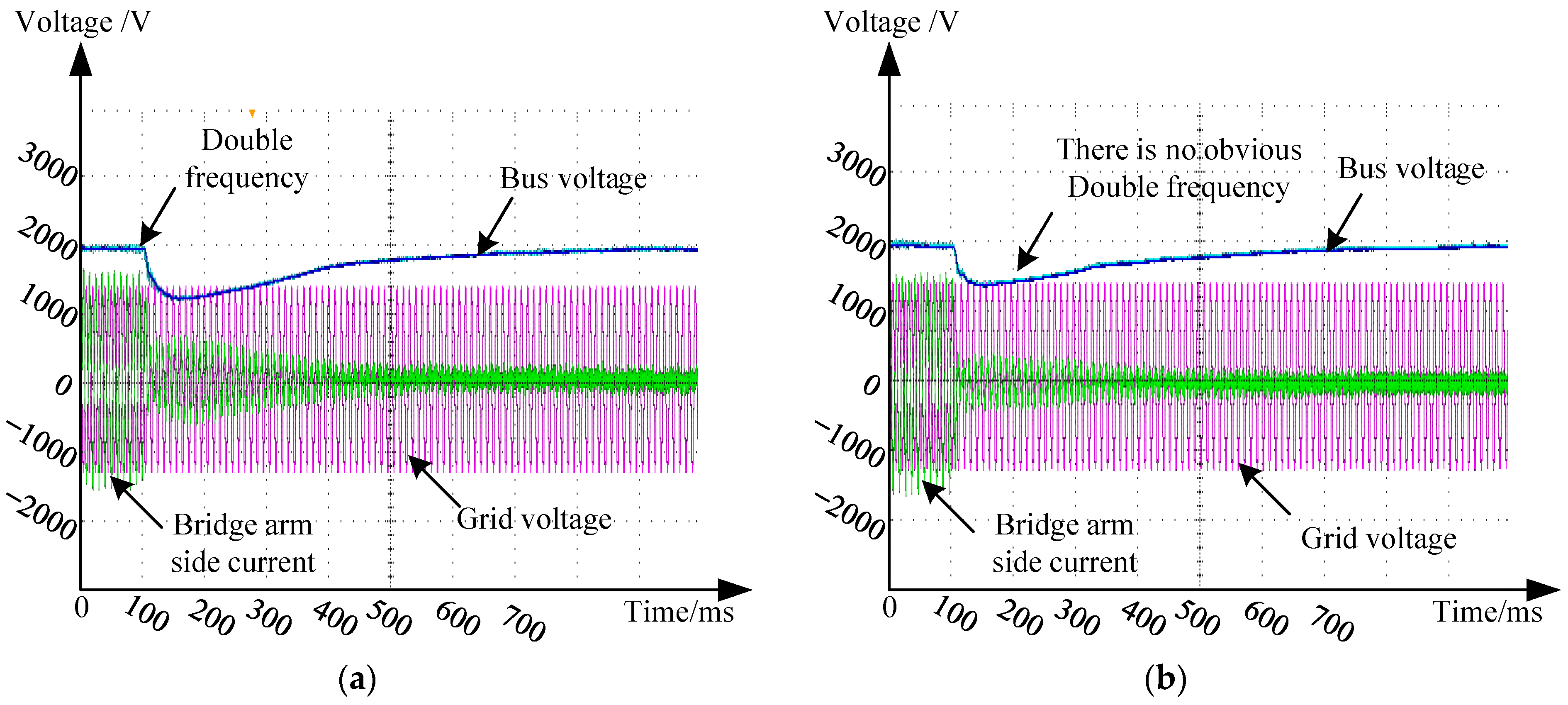
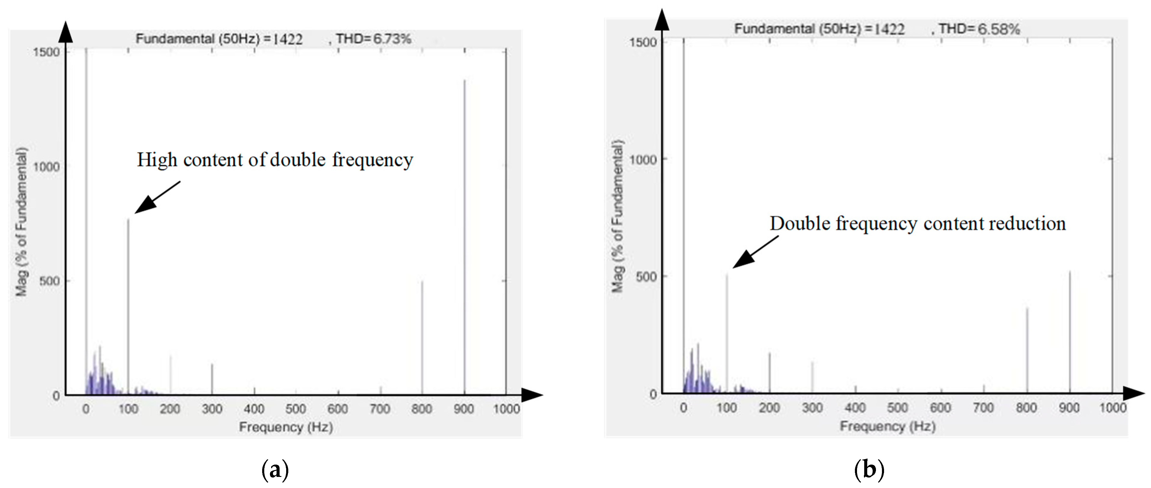
4. Simulation and Experimental Results

The mathematical model of the delay-free adaptive state observer constructed for extracting the DC component of the DC bus voltage is in the form of a state space equation. There are two undetermined parameters, m and n, in this state space equation, and the value of n will directly affect the estimation error of the state observer for the observation target. Through repeated experimental verification, it was found that n is in the (0.9, 1.05) interval, and the observation error is stable within a small range. The adaptive state observer designed in this paper does not need to introduce delay, but it is a nonlinear system, so its stability is verified by the Lyapunov theorem. The choice of parameter m directly affects the construction of the stability criterion. The parameter conditions to ensure the stability of the observer are given in this paper. As long as the appropriate m is selected according to these conditions, the observer can work stably, and can be used to eliminate the second harmonic interference in the DC bus voltage, so as to be connected to the closed-loop control system.

Simulation Experiment of Disturbance Suppression Control Strategy on Rectification Side of Power Unit

Experiments were conducted on the effect of adding an adaptive state observer to the second harmonic suppression control strategy on the dynamic and steady-state performance of a PWM rectifier under a rated input voltage of 1900 V.
Using the starsim real-time simulator, based on the back-to-back H-bridge model, and using FPGA technology, the system’s real-time simulation with a 100-microsecond step size and any working condition is realized. Use the starsim HIL 5.3.0 upper computer software to load the motor simulation topology of the cophase power supply system into the real-time simulator and correctly connect the interface of the real-time simulator with the motor controller interface, so that the real-time control can be implemented. As shown in Figure 9.
In the no-load state shown in Figure 10 and Figure 11, the step change in grid voltage will be directly transmitted to the bus terminal through the system impedance. When no control strategy is applied, the instantaneous disturbance of the grid voltage will cause a second harmonic fluctuation of the bus voltage (waveform display ± 5% ripple). After applying the suppression strategy, the waveform shows a significant decrease in the amplitude of the second harmonic of the bus voltage (such as dropping below ± 1%). This indicates that the control algorithm effectively offsets the power imbalance caused by grid disturbances by adjusting the output power of the inverter in real-time.
When loaded as shown in Figure 12 and Figure 13, the dual disturbance of grid voltage fluctuations and load power demand will exacerbate the second harmonic fluctuations of bus voltage (as shown in waveform oscillations). The experimental waveform shows that under the suppression strategy, the amplitude of the second harmonic fluctuation of the bus voltage is reduced to a negligible range (such as ± 1%), and the oscillation is largely eliminated.
The proposed suppression strategy effectively mitigates transient voltage deviations caused by abrupt load changes. During sudden load increases (Figure 14 and Figure 15), it reduces the peak voltage drop from 5% to 1% by dynamically compensating power deficits, while suppressing 92% of second harmonic ripples through active filtering. Conversely, during load shedding, the strategy limits voltage surges to <1.2% and eliminates energy feedback-induced harmonics by regulating regenerative current paths. This dual-action control ensures waveform flatness (THD < 3%) across both transient scenarios.
It can be seen from Figure 16 that by adding the suppression control strategy, the harmonic content of input current IL is reduced by 0.15%, which enhances the dynamic response ability of the system to input voltage disturbance and reduces the fluctuation of DC bus voltage caused by input voltage disturbance. After adding the suppression strategy, the analysis of total harmonic distortion (THD) by fast Fourier transform (FTT) shows that the second harmonic component in the DC bus voltage is significantly reduced. The spectrum results of the THD show that the dominant second harmonic amplitude is significantly reduced, which verifies the effectiveness of the suppression strategy. This improvement effectively weakens the impact of double frequency fluctuation on the system, and provides important support for the stability of the control system and the improvement of power quality.

5. Conclusions

The simulation experiment of the rectifier side delay-free adaptive compensation control strategy for the power unit topology of the new in-phase power supply system for electrified railways, including grid voltage, DC bus current, and DC bus voltage doubling suppression function, shows that the doubling resonance suppression control strategy is effective and reduces the fluctuation of DC bus voltage caused by input voltage disturbance. The proposed delay-free adaptive state observer has been demonstrated to effectively suppress dual line frequency ripple in laboratory-scale simulations. The key experimental verification and coverage of multiple scenarios, such as power grid disturbances and load changes, show that the waveform consistency indicates that the strategy can effectively suppress second harmonic fluctuations under different operating conditions, verifying its robustness. By optimizing the topology and simplifying the hardware, the auxiliary power supply decoupling circuit control algorithm has been eliminated to achieve second harmonic ripple attenuation, without the need for additional filtering components to maintain system stability under typical traction load changes.
  • Engineering impact:
It provides a cost-effective solution for the transformation of the existing cophase power supply system, meets the requirements of reducing harmonics, reduces the size of capacitors, and proves that the traction power supply is compatible.
  • Economic potential:
Preliminary analysis shows that the maintenance frequency of the generator set has been reduced by 15% through ripple mitigation, and the expected lifespan of the DC link capacitor has been extended by 20%, providing a theoretical basis for the development of modular traction substations.
  • Limitations of Research and Future Work:
Experimental verification is currently limited to simulating the long-term reliability of a single power supply unit and requires further hardware-in-the-loop testing.
Economic benefits need to be verified on-site in actual railway operations, such as multi-unit parallel operation testing under a load curve, implementation of a real-time performance evaluation controller based on FPGA, and cooperation with locomotive and vehicle manufacturers for system-level integration.

Author Contributions

Conceptualization, J.Z. and Y.L.; methodology, J.Z.; software, Y.L.; validation, J.Z. and Y.L.; formal analysis, Y.L.; data curation, Y.L.; writing—original draft preparation, Y.L.; writing—review and editing, Y.L.; visualization, Y.L.; supervision, J.Z. All authors have read and agreed to the published version of the manuscript.

Funding

This paper was funded by the Beijing Municipal Natural Science Foundation (L242007).

Data Availability Statement

No new data were created or analyzed in this study.

Conflicts of Interest

The authors declare no conflicts of interest.

References

  1. Min, Y.; Ke, C. Research Review on Topology and Control Strategy of Energy Storage Connected to Electrified Railway. High Volt. Eng. 2023, 49, 4069–4083. [Google Scholar]
  2. Zhou, L. Second Harmonic Injection with Model Predictive Control: Attenuation of DC-Link Pulsations in Single-Phase Inverters. IEEE Trans. Power Electron. 2025, 40, 6529–6538. [Google Scholar] [CrossRef]
  3. Yan, X.; Li, B. Single-Phase Dual Rotary Phase Shifting Transformer Based Negative Sequence Compensation Method for High-Speed Railway Systems. Trans. China Electrotech. Soc. 2024, 39, 1029. [Google Scholar]
  4. Zhao, L. Research on Integrated Compensation System of Electrified Railway Supplied by the Scott Hypotenuse. Doctoral Dissertation, Beijing Jiaotong University, Beijing, China, 2023. [Google Scholar]
  5. Zhou, J.; Pan, Y. Power Unit Control Strategy of the New Type Cophase Power Supply Topology. Electr. Transm. 2014, 44, 36–41. [Google Scholar]
  6. Zhang, J.; Xu, Y.; Li, Y. Completed compensation strategy research of railway power conditioner for negative-sequence current under unbalanced AC power grids. Proc. CSEE 2020, 40, 3144–3154. [Google Scholar]
  7. Shu, Z.; Xie, S.; Li, Q. Single-Phase Back-To-Back Converter for Active Power Balancing Reactive Power Compensation and Harmonic Filtering in Traction Power System. IEEE Trans. Power Electron. 2011, 26, 334–343. [Google Scholar] [CrossRef]
  8. Zhang, C.; Chen, B.; Yuan, J.; Zhong, Y.; Tian, C.; Cai, C. Research on Hybrid Compensation of Power Quality in Same Phase Power Supply System Based on V/V Traction Transformer. J. Electr. Eng. 2015, 30, 496–504. [Google Scholar]
  9. He, X.; Shu, Z.; Peng, X.; Zhou, Q.; Zhou, Y.; Zhou, Q.; Gao, S. Advanced Cophase Traction Power Supply System Based on Three-Phase to Single-Phase Converter. IEEE Trans. Power Electron. 2014, 29, 5323–5332. [Google Scholar] [CrossRef]
  10. Shu, Z.; Xie, S.; Lu, K.; Zhao, Y.; Nan, X.; Qiu, D.; Zhou, F.; Gao, S.; Li, Q. Digital Detection Control and Distribution System for Co-phase Traction Power Supply Application. IEEE Trans Ind. Electron. 2013, 60, 1831–1839. [Google Scholar] [CrossRef]
  11. Cheng, R.; Ding, S.; Jiang, Z.; Ma, Z.; Wang, Y.; Jiang, W.; Liu, C.; Li, J.; Li, G.; Fu, D.; et al. Railway Traction AC in-Phase Power Supply Device Based on Three-Phase Series Voltage Source Symmetrical Transformation. Chinese Patent 101345483A, 31 January 2012. [Google Scholar]
  12. Li, Z.; Zhang, H. New continuous co-phase traction power supply converter system based on power electronic transformer. Adv. Technol. Electr. Eng. Energy 2018, 37, 3394–3401. [Google Scholar]
  13. Guo, X.; Wu, W. Comparative Analysis and Digital Implementation of Novel Control Strategies for Grid-Connected Inverters. Trans. China Electrotech. Soc. 2007, 22, 111–116. [Google Scholar]
  14. Huang, X.; Li, Q. Control strategy of co-phase traction power supply system and simulative analysis. Electr. Power Autom. Equip. 2014, 34, 2006–2014. [Google Scholar]
  15. Zhao, Y.; Zhu, P.; Qunzhan, L. Co-phase supply test system based on YNvd balanced transformer and simulated load. Power Syst. Prot. Control 2016, 44. [Google Scholar]
  16. Xu, T.; Yingdong, W.; Qirong, J. A Railway Unified Power Quality Controller Based on Modular Structure for Electric Railway. Autom. Electr. Power Syst. 2012, 36, 101–106. [Google Scholar]
  17. Yao, J.; Zhang, T. Impacts of Negative Sequence Current and Harmonics in Traction Power Supply System for Electrified Railway on Power System and Compensation Measure. Power Syst. Technol. 2008, 39, 61. [Google Scholar]
  18. Li, X. Research on Anti-Load Disturbance of Three Level Dual Pwm Converter Based on Dc Bus Current Reconstruction. Master’s Thesis, Xi’an University of Technology, Beilin, China, 2016. [Google Scholar]
Figure 1. The topological structure of the power unit in the new type of cophase power supply.
Electronics 14 02047 g001
Figure 2. Structure diagram of a delay-free adaptive state observer.
Electronics 14 02047 g002
Figure 3. Circuit diagram of the single-phase PWM rectifier.
Electronics 14 02047 g003
Figure 4. Physical model of single-phase PWM rectifier.
Electronics 14 02047 g004
Figure 5. Current inner loop control block diagram.
Electronics 14 02047 g005
Figure 6. Voltage outer loop control diagram.
Electronics 14 02047 g006
Figure 7. Voltage outer loop control diagram with load current i0 feedforward control added.
Electronics 14 02047 g007
Figure 8. Double closed-loop control block diagram with no delay adaptive state observer added.
Electronics 14 02047 g008
Figure 9. Semi-physical simulation platform for single-phase H-bridge control system of the power unit.
Electronics 14 02047 g009
Figure 10. No-load drop low grid voltage output voltage current waveform: (a) No suppression strategy; (b) add suppression strategy.
Electronics 14 02047 g010
Figure 11. Waveform diagram of output voltage and current for increasing grid voltage under no-load conditions: (a) No suppression strategy; (b) add suppression strategy.
Electronics 14 02047 g011
Figure 12. Waveform diagram of output voltage and current for reducing grid voltage under load: (a) No suppression strategy; (b) add suppression strategy.
Electronics 14 02047 g012
Figure 13. Waveform diagram of output voltage and current for increasing grid voltage under load: (a) No suppression strategy; (b) add suppression strategy.
Electronics 14 02047 g013
Figure 14. Voltage and current waveform diagram under sudden increase in load: (a) No suppression strategy; (b) add suppression strategy.
Electronics 14 02047 g014
Figure 15. Voltage and current waveform diagram under sudden load reduction: (a) No suppression strategy; (b) add suppression strategy.
Electronics 14 02047 g015
Figure 16. IL harmonic analysis: (a) No suppression strategy; (b) add suppression strategy.
Electronics 14 02047 g016
Disclaimer/Publisher’s Note: The statements, opinions and data contained in all publications are solely those of the individual author(s) and contributor(s) and not of MDPI and/or the editor(s). MDPI and/or the editor(s) disclaim responsibility for any injury to people or property resulting from any ideas, methods, instructions or products referred to in the content.

