Article

Efficiency-Enhanced Hybrid Dickson Converter with Quasi-Complete Soft Charging for Direct Large-Ratio Step-Down Applications

1
School of Electrical and Information Engineering, Zhengzhou University, Zhengzhou 450001, China
2
School of Electrical and Information Engineering, North Minzu University, Yinchuan 750021, China
*
Author to whom correspondence should be addressed.
Electronics 2025, 14(10), 2001; https://doi.org/10.3390/electronics14102001
Submission received: 9 April 2025 / Revised: 8 May 2025 / Accepted: 9 May 2025 / Published: 14 May 2025

Abstract

:
This article presents an efficient non-isolated DC-DC hybrid converter for direct large-ratio step-down applications such as data centers. The converter topology employs a three-level-assisted Dickson switched capacitor network and interleaved dual inductors, significantly mitigating voltage swings at the switching nodes. As a result, the conduction duration of rectifying switches is substantially extended. This configuration is suitable for both odd- and even-order converters, achieving self-balancing of the flying capacitor voltages and inductor currents. To address uneven interleaved inductor currents, a duty-cycle-matching-based current distribution method is proposed to ensure equal current sharing and facilitate loss transfer between inductors. Additionally, an intrinsic charge-ratio-based method for capacitance optimization is introduced to achieve quasi-complete soft charging of the flying capacitors. This method eliminates surge currents during reconfiguration of the capacitor network, reduces losses, and enhances the capacitor utilization. Operating at 300 kHz, the prototype achieves high-ratio voltage conversion from 48 V to 0.5–2.0 V, with a maximum output current of 30 A. It attains a peak efficiency of 91.96% and a power density of 944.88 W/in3. Quasi-complete soft charging of the flying capacitors results in an approximate 2.94% improvement in the conversion efficiency.

1. Introduction

With the rapid progression of big data, cloud computing, and artificial intelligence, the power consumption in data centers is experiencing explosive growth. According to the International Energy Agency, the energy consumption of data centers was approximately 460 TWh in 2022 and is projected to reach 800 TWh by 2026 [1]. To reduce significant ohmic losses in the power bus, the 48 V distributed power supply architecture has progressively replaced the traditional 12 V system [2,3]. However, converting the nominal 48 V bus voltage into the ∼1 V core voltage required by CPUs and GPUs presents a major challenge for the design of point-of-load (PoL) converters due to the large voltage conversion ratio. Additionally, with the surge in the demand for computational power, the operating current in digital systems has escalated to tens or even hundreds of amperes. Consequently, for the converters utilized in data centers to support low-voltage rails and high-output currents, maintaining a high conversion efficiency and effectively handling large-ratio voltage conversion are critical performance requirements [4,5].
The traditional Buck converter experiences extremely narrow switch-on times due to a large step-down ratio. In 48 V-to-1 V conversion with a duty cycle of ∼0.02 and a frequency of hundreds of kHz, the power switches’ ON time becomes comparable to their turn-on delay, making precise control of the output voltage difficult. Moreover, the short ON time also results in a large root mean square (RMS) current and increased loss. A two-stage conversion architecture addresses the significantly increased step-down ratio by retaining the original 12 V conversion module and introducing a mature 48 V-to-12 V pre-conversion unit in series [6,7,8]. This configuration allows for the rapid integration of existing modules to meet the application requirements. However, the overall conversion efficiency is limited because of the cascaded power transmission. Additionally, stacked structures, such as the single-stage sigma converter, integrate a fixed-ratio DC-DC converter with a Buck converter, both of which share the same input voltage [9,10,11]. The entire variation in the input voltage is absorbed by the Buck converter, while the output voltage is regulated by adjusting the duty cycle. The sigma converter achieves a peak efficiency of 94% in 48 V-to-1 V conversion [9]. However, this converter requires two separate power conversion circuits operating at different frequencies, which increases the system complexity.
In recent years, hybrid converters combining switched-capacitor (SC) and switched-inductor techniques have garnered significant interest among researchers. These converters employ flying capacitors and magnetic components to achieve continuously adjustable large-ratio voltage conversion. This approach reduces the voltage stress on the switching devices and takes full advantage of the high energy density of multilayer ceramic capacitors (MLCCs) [12]. Additionally, hybrid converters utilize the current suppression effect of magnetic components to prevent large surge currents through the flying capacitors, ensuring soft charging [13]. Compared to traditional switched-inductor converters (such as Buck converters), hybrid converters significantly lower the volt-second product of the magnetic components, thereby considerably reducing the inductance and size [14]. Among these hybrid converters, flying capacitor multilevel (FCML) converters stand out by employing multiple symmetrically distributed flying capacitors. This design effectively reduces the voltage swing at the output node of the capacitor network, achieving a high voltage conversion ratio [15,16,17]. However, FCML converters encounter a charge balancing issue with the flying capacitors, necessitating dedicated control methods, as described in [15], which increases the complexity of system control. Due to its superior V-A rating for the switch, the Dickson topology offers the best switch utilization compared to that of similar topologies [14,18,19], allowing the converter to use low voltage-rated switches with better figures of merit [20]. Consequently, the Dickson topology has attracted widespread attention, and numerous research publications have emerged. Related derivative topologies include the hybrid Dickson (HD) converter [21,22], the dual-inductor hybrid Dickson (DIH) converter [23,24,25,26], and the symmetrical dual-inductor hybrid Dickson (SDIH) converter [27,28,29]. Critical insights into the limitations of the existing topologies can be systematically derived from prior studies [21,22,23,24,25,26,27,28,29]. Specifically, the cited works collectively reveal two fundamental challenges: (i) conduction path inefficiencies and intrinsic balancing constraints in HD converters, and (ii) inadequate duty cycle extension ratios in DIH and SDIH implementations. The N-order HD converter can achieve an N/2-fold duty cycle extension. However, the output current flows through the series freewheeling switches, which results in significant conduction losses. Moreover, not all flying capacitors can be self-balanced, so additional control is needed in practical applications. Compared to an HD converter, the N-order DIH and SDIH converters double the ON time. The SDIH converter, due to its symmetrical structure with two input paths, provides stronger power conversion capabilities but also doubles the number of switches and flying capacitors.
The split-phase control proposed in [21] enables complete soft charging of the flying capacitors, allowing for larger voltage ripples and thus enhancing their utilization. Additionally, complete soft charging of the capacitors helps prevent spike currents during the dynamic reconfiguration of the switched-capacitor network, thereby eliminating the associated losses. This split-phase method has been applied to a DIH converter [24] and an SDIH converter [29]. However, the precise phase-shift timing depends on factors such as the inductance, switching frequency, load current, and output voltage. Therefore, this method necessitates gathering multiple electrical parameters and employing a controller with a high computational performance. Furthermore, in extreme-voltage-conversion-ratio applications (e.g., 60 V to 0.5 V), the theoretical duty cycle of a six-order DIH or SDIH converter is only 0.05, which is clearly not favorable for system control.
To address the aforementioned issues, this article presents a quasi-complete soft charging three-level-assisted hybrid Dickson (QCSC-TLAHD) topology with dual inductors, as illustrated in Figure 1. The primary contributions are as follows:
(1)
The proposed N-order hybrid Dickson converter extends the switch duty cycle by a factor of (2N-1), demonstrating a significant improvement over the N-fold and N/2-fold duty cycle expansions in DIH and HD converters.
(2)
An intrinsic charge-ratio-based capacitance optimization method is proposed to achieve quasi-complete soft charging of the flying capacitors, thereby minimizing the spike currents during capacitor network reconfiguration, optimizing the efficiency, and enhancing the capacitor utilization.
(3)
To address the unequal inductor currents, a duty-cycle-matching-based current equalization method is proposed. By adjusting the PWM duty cycle ratio, the average currents are equalized, ensuring a balanced loss distribution between inductors.
(4)
This topology can be applicable to odd- and even-order converters, overcoming the limitations of DIH converters in [23,24]. Moreover, it ensures self-balancing of the voltages and inductor currents of all flying capacitors.
The rest of this article is structured as follows. Section 2 details the circuit operation and steady-state characteristics of the proposed QCSC-TLAHD converter. Section 3 presents the method for equalizing the inductor currents and offers a comparative analysis of the inductor losses. Section 4 proposes the intrinsic charge-ratio-based capacitance optimization method, extends this method to an N-order converter, and provides guidelines for the capacitor selection. The results of experimental validation of the converter prototype are presented in Section 5. Finally, Section 6 concludes this article.

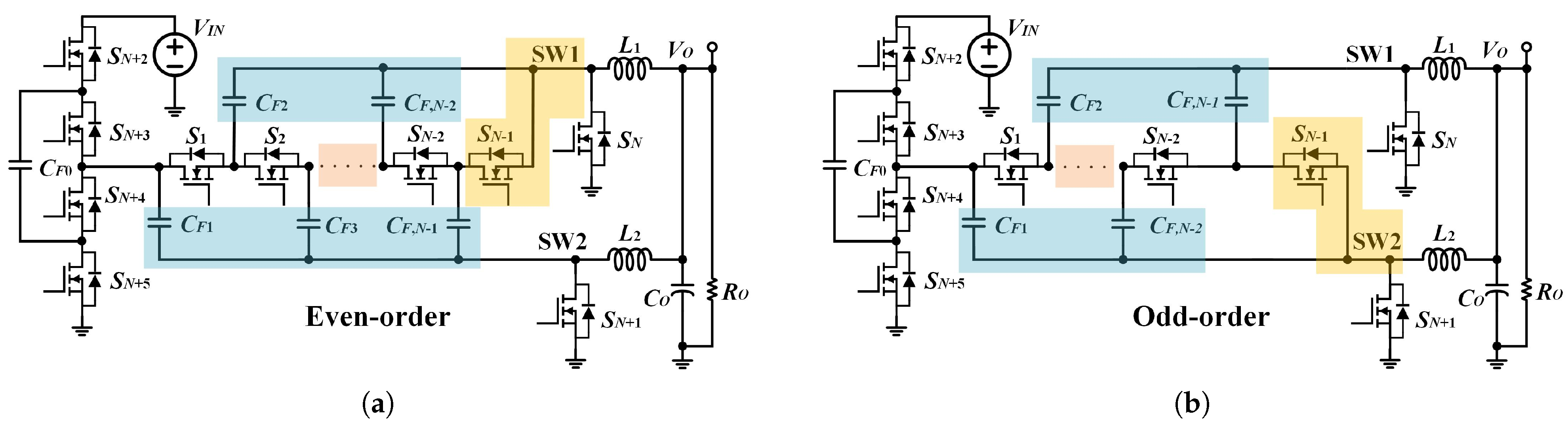
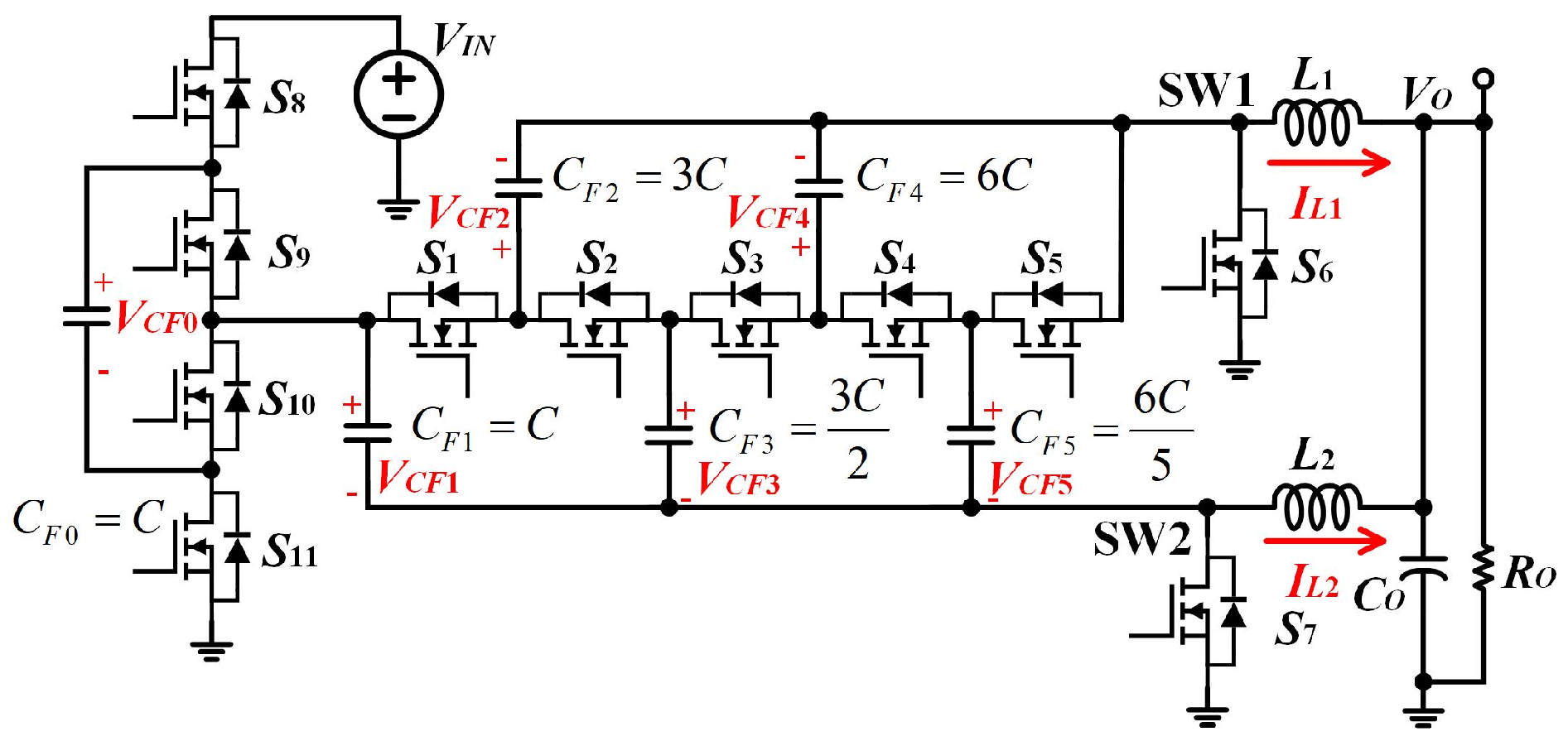
2. The Proposed Converter

The proposed QCSC-TLAHD topology comprises N + 5 power switches ( S 1 S N + 5 ), N flying capacitors ( C F 0 C F , N 1 ), and two output inductors ( L 1 , L 2 ), as depicted in Figure 1. The interconnections of the power devices differ between even- and odd-order QCSC-TLAHD converters. In even-order converters, as shown in Figure 1a, N 2 2 and N 2 flying capacitors are connected to L 1 and L 2 , respectively, with S N 1 connected to L 1 , whereas in odd-order converters, each inductor is connected to N 1 2 flying capacitors, with S N 1 connected to L 2 , as illustrated in Figure 1b. These variations directly result in differing amounts of charge transfer and paths in the capacitor networks of the even- and odd-order converters.

2.1. Principle of Operation

This section explores the operating principle of the proposed topology using a six-order QCSC-TLAHD converter, as shown in Figure 2. The converter consists of 11 power switches ( S 1 S 11 ), 6 flying capacitors ( C F 0 C F 5 ), and 2 inductors ( L 1 , L 2 ). During one working period T S , the converter undergoes four operation phases ( Φ 1 Φ 4 ), with the corresponding equivalent circuits and ideal operational waveforms illustrated in Figure 3. The figures detail the ON-OFF states of the switches, the charging and discharging of the capacitors, and the variations in the current in the inductors. Based on the operating phases, the active components are divided into two groups, with each working with a 180-degree shift: (1) rectifying switches S 2 , S 4 , S 8 , and S 10 and the freewheeling switch S 6 and (2) rectifying switches S 1 , S 3 , S 5 , S 9 , and S 11 and the freewheeling switch S 7 . These switches manage the charging and discharging of the flying capacitors. As shown in Figure 3d, the duty cycles of the drive pulses for switches S 1 , 3 , 5 , 9 , 11 and S 2 , 4 , 8 , 10 are D 1 and D 2 . The drive signals for the freewheeling switches S 6 and S 7 , in turn, are complementary to these two signals, respectively. For simplification, the dead time is ignored. Due to the DC blocking effect of the capacitors, the voltage swings V S W 1 , 2 at switch nodes SW1 and SW2 are reduced significantly, effectively addressing the issue of an extremely small duty cycle under a high voltage conversion ratio. Assume the voltages of the flying capacitors C F 0 C F 5 are v C F 0 v C F 5 , with their steady-state DC bias voltages denoted as V C F 0 V C F 5 . The currents i L 1 and i L 2 in inductors L 1 and L 2 increase and decrease alternately with a 180-degree phase shift. Although the following analysis is based on an even-numbered six-order QCSC-TLAHD converter as an example, the process can be extended to other N-order converters.
During phase Φ 1 , depicted in Figure 3a, all even-indexed switches S 2 , 4 , 6 , 8 , 10 are activated, establishing three parallel capacitor branches ( ( C F 0 C F 1 ) ( C F 2 C F 3 ) ( C F 4 C F 5 ) ), where the operators ‘–’ and ‘‖’ denote series and parallel connections of the capacitors, respectively. Charge flows through these capacitors to the inductor L 2 , where C F 2 and C F 4 discharge. Under the influence of a positive magnetizing voltage, the current i L 2 experiences an approximately linear increase. Meanwhile, with S 6 in the ON state, L 1 undergoes a linear decrease in current due to the reverse voltage V O applied across it, where V O represents the output voltage. Under the inductor’s current suppression effect, the currents traversing C F 0 5 deviate from those observed in traditional SC converters. The charging and discharging process for the flying capacitors is regulated by currents proportional to i L 2 , thus enabling gentle operation. However, during the instantaneous state transition of the power switches, surge currents may occur, stemming from terminal voltage imbalances across the reconstructed parallel capacitor branches. These deviations cause charge redistribution phenomena, resulting in instantaneous hard charging and discharging of the capacitors with additional losses. Further elaboration on this phenomenon will be provided in Section 4.
After Φ 1 lasting for D 2 T S , the converter switches to Φ 2 , as illustrated in Figure 3c, for a duration of 0.5 D 2 T S . During this phase, all power switches, except for S 6 and S 7 , are deactivated, maintaining the charge on the flying capacitors. With the activation of S 6 and S 7 , the reverse magnetizing voltage V O is applied to inductors L 1 and L 2 , initiating the demagnetization process and resulting in linear current decay.
Following half of the operating period comprising Φ 1 and Φ 2 , the converter enters Φ 3 (lasting for D 1 T S ), as shown in Figure 3b. The odd-numbered switches S 1 , 3 , 5 , 9 , 11 are activated, while S 6 is deactivated. A new capacitor network is formed: ( ( C F 0 C F 1 ) C F 2 ) ( C F 3 C F 4 ) C F 5 . The charge through these capacitors is injected into the inductor L 1 . Subsequently, L 1 experiences the magnetization process, causing the current i L 1 to increase approximately linearly. The charge accumulated in C F 0 , 1 , 3 , 5 during Φ 1 is released. Upon the completion of Φ 3 , only S 6 and S 7 conduct again, and the converter transitions into Φ 4 , resembling Φ 2 , with a duration of 0.5 D 1 T S .

2.2. Steady-State Characteristics

Under steady-state conditions, assume a small voltage ripple across the flying capacitors. As shown in Figure 3a,b, according to the Kirchhoff’s voltage law (KVL), the relationship among the average voltages V C F 0 5 across the flying capacitors and the voltage swings V S W 1 , 2 on switching nodes SW1 and SW2 can be described by
V I N V C F 0 V C F 1 = V C F 2 V C F 3 = V C F 4 V C F 5 = V S W 2 V C F 1 V C F 2 = V C F 3 V C F 4 = V C F 5 = V S W 1 V C F 0 = V C F 1 ,
where V I N is the input voltage. The inductors L 1 and L 2 follow the volt-second balance principle, i.e., V S W 1 V O D 1 T S = V O 1 D 1 T S , V S W 2 V O D 2 T S = V O 1 D 2 T S , which can be simplified as
V S W 1 = V O D 1 V S W 2 = V O D 2 .
When the converter operates for the same duration in Φ 1 and Φ 3 , i.e., D 1 = D 2 = D , substituting this condition into (2) yields V S W 1 = V S W 2 . Using this result in (1) subsequently derives
V C F 0 = V C F 1 = 5 V I N 11 V C F 2 = 4 V I N 11 V C F 3 = 3 V I N 11 V C F 4 = 2 V I N 11 V C F 5 = V S W 1 = V S W 2 = V I N 11 .
Substituting the equal V S W 1 and V S W 2 , along with the duty cycle D, back into (2) results in the output voltage V O as follows:
V O = D V I N 11 .
From (3), the maximum average voltage of the flying capacitors is V C F 0 = V C F 1 = 5 V I N 11 , which is much lower than that of DIH converters, where the voltage is close to V I N [24,25]. This low working voltage contributes to miniaturization of the capacitor volume and enables the use of low-equivalent-series-resistance (ESR) MLCCs as flying capacitors in the converter. The voltage swings V S W 1 and V S W 2 are compressed to only 1/11 of V I N . The reduction in the node voltage facilitates the expansion of the converter duty cycle, with an 11-fold extension in the six-order converter as (4). Furthermore, a reduced voltage swing enables the use of a smaller inductance due to the diminished volt-second product, effectively decreasing the inductor volume and optimizing the power density. Additionally, as the duty cycle increases, the effect of interleaved inductors in reducing ripples in the output current is strengthened, which further reduces the required inductance and size [30].
Assume the charge from V I N within one operating cycle is q, corresponding to the input charge in Φ 1 , as shown in Figure 3a. In a steady state, all of the flying capacitors must maintain charge balance between Φ 1 and Φ 3 . This means the charge added in one phase must be fully released in the other. Thus, within one period, the transferred charge for C F 0 , 1 and C F 2 5 is q and 2q, respectively. The charge passing through L 2 in Φ 1 is 5q, and that through L 1 in Φ 3 is 6q. Therefore, the average currents of L 1 and L 2 can be expressed as
I L 1 = 6 q D 1 T S ,
I L 2 = 5 q D 2 T S .
Given that the output current I O flows entirely through inductors L 1 and L 2 , and assuming D 1 = D 2 = D , the unequal average currents in these two inductors can be represented as follows:
I L 1 = 6 11 I O ,
I L 2 = 5 11 I O .
The derivation process from (1) to (8) is also applicable to an N-order converter, where N can be either odd or even. The average voltages V C F , j across the flying capacitors and the node voltage swings V S W 1 , 2 can be derived as
V C F , j = N 1 2 N 1 V I N , j = 0 N j 2 N 1 V I N , j 1 , N 1 ,
V S W 1 = V S W 2 = V I N 2 N 1 .
The voltage conversion ratio M can be expressed as
M = V O V I N = D 2 N 1 .
According to (11), the proposed converter achieves a duty cycle extension by a factor of 2 N 1 . Figure 4 illustrates that the Buck converter exhibits a significantly small duty cycle under large-ratio voltage conversion. For the same ratio M, the duty cycle of the QCSC-TLAHD converter is almost twice that of the DIH converter [24]. This feature allows for precise output voltage control.
When the inductors L 1 and L 2 in Figure 1 operate in freewheeling mode (in Φ 2 , 4 ), they experience a reverse magnetizing voltage of V O . In a steady state, the variation in the inductor current during this duration constitutes the current ripple. By applying the induced voltage formula combined with (11), the current ripples Δ I L 1 and Δ I L 2 can be determined as
Δ I L 1 = Δ I L 2 = V O 1 D T S L = V O 1 2 N 1 M T S L ,
where L is the inductance of L 1 and L 2 .
In phases Φ 1 and Φ 3 , different capacitor networks are constructed, and L 1 and L 2 conduct different amounts of charge. When N is even, there are N 2 parallel capacitor branches in both phases Φ 1 and Φ 3 , through which the charges of N q and N 1 q are transferred to L 1 and L 2 , respectively. For odd N, in phase Φ 1 , N q charge flows into L 2 via N + 1 2 parallel capacitor branches, while in Φ 3 , N 1 q charge is transferred to L 1 through N 1 2 parallel paths. Therefore, the average currents of inductors L 1 and L 2 can be described as
I L , k | N = E v e n = N q D 1 T S , k = 1 ( N 1 ) q D 2 T , k = 2 ,
I L , k | N = O d d = ( N 1 ) q D 1 T S , k = 1 N q D 2 T S , k = 2 .
When D 1 = D 2 = D , the average currents can be derived as
I L , k | N = E v e n = N 2 N 1 I O , k = 1 N 1 2 N 1 I O , k = 2 ,
I L , k | N = O d d = N 1 2 N 1 I O , k = 1 N 2 N 1 I O , k = 2 .
From (9), (15), and (16), it can be observed that in the steady state, the converter achieves self-balancing of the flying capacitors without additional control circuits or methods, and the average currents of the inductors automatically converge to a specific proportion of the output current.

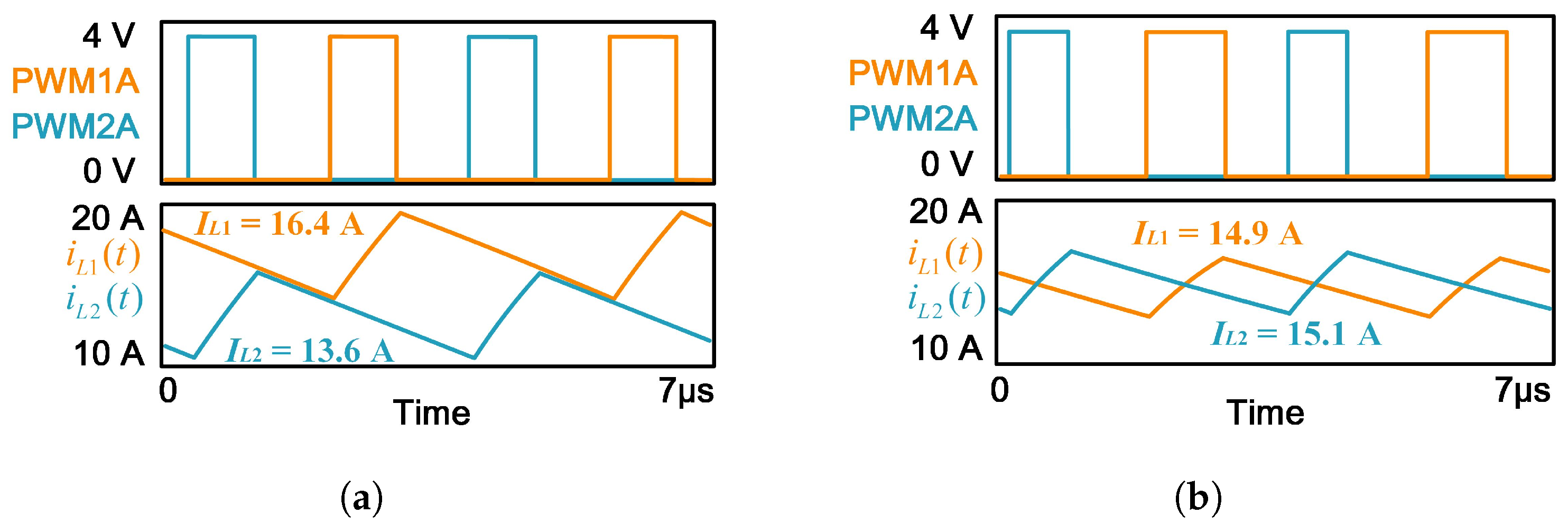
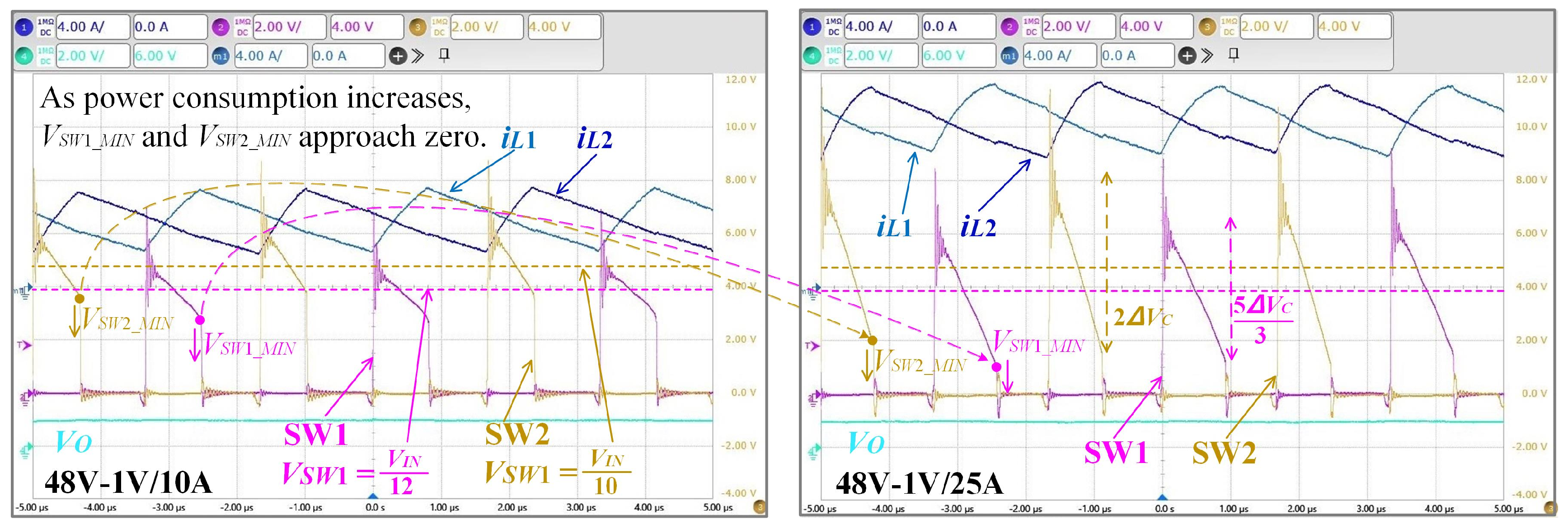
3. Equalization of the Inductor Current

In the proposed hybrid converter, inductors L 1 and L 2 collectively carry the output current I O . According to Equations (15) and (16), while the inductor currents can automatically adjust to match the output current, I L 1 and I L 2 exhibit inequality. As the order N decreases, the disparity between I L 1 and I L 2 becomes more pronounced. For example, in six-, five-, and four-order QCSC-TLAHD converters, I L 1 surpasses I L 2 by approximately 20%, −20%, and 33.3%, respectively. This imbalance in the inductor currents poses challenges in the device selection and leads to additional losses. Therefore, it is necessary to ensure that the inductor currents are equalized.

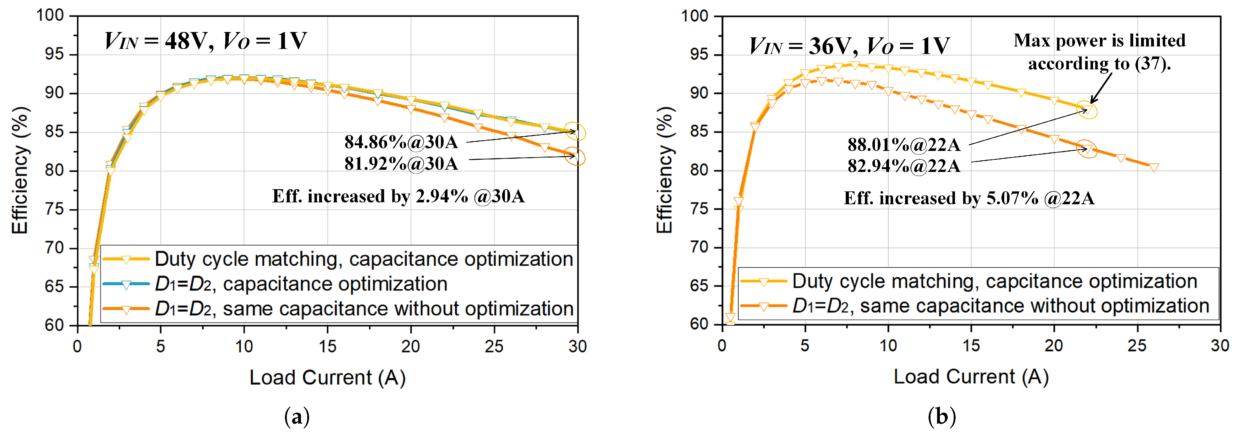
3.1. A Duty-Cycle-Matching-Based Current Equalization Method

The analysis from (15) and (16) indicates that the average current distribution in inductors L 1 and L 2 varies with the order of the converter. Specifically, in even-order converters, I L 1 exceeds I L 2 , while the opposite is true for odd-order ones. From (13) and (14), it is observed that adjusting the ratio between D 1 and D 2 (duty cycle matching) can effectively promote the equality of I L 1 and I L 2 . For even-order converters, setting D 1 D 2 = N N 1 , and for odd-order ones, setting D 1 D 2 = N 1 N , results in I L 1 = I L 2 = I O 2 .
Under steady-state conditions, inductors L 1 and L 2 adhere to the volt-second balance principle, with V S W 1 and V S W 2 satisfying (2). During Φ 1 and Φ 3 , according to KVL, the relationship among the capacitor’s average voltages V C F 0 V C F , N 1 and the node swings V S W 1 , 2 resembles (1). Various parameters of the converter in cases of duty cycle mismatching ( D 1 = D 2 ) and matching are presented in Table 1, with the derivation process referenced in Section 2.2. Given that power switches with duty cycles D 1 and D 2 are directly interconnected within the electrical structure, it is imperative to satisfy the constraint D 1 + D 2 < 1 . Otherwise, concurrent conduction of the switches may ensue, leading to component damage.
From Table 1, it is evident that to equalize the average inductor current, even-order converters require D 1 = 2 N M and D 2 = 2 N 1 M , while odd-order configurations necessitate D 1 = 2 N 1 M and D 2 = 2 N M , with D 1 and D 2 exhibiting symmetry. In microcontrollers with high-precision PWM outputs, a proportional relationship between D 1 and D 2 corresponding to the converter order N is readily achievable. Similarly, other parameters of even- and odd-order converters, such as the average voltages V C F , j of the flying capacitors, the node voltage swings V S W 1 , 2 , and the ripples in the inductor current Δ I L 1 , 2 , also demonstrate apparent symmetry once the duty cycles are matched.
Figure 5 depicts simulated waveforms of the inductor currents for the six-order QCSC-TLAHD converter operating at 300 kHz and 48 V-to-1 V with a 30 A load. When D 1 = D 2 , it is evident that I L 1 > I L 2 . After duty cycle matching, I L 1 and I L 2 are approximately equal, demonstrating that matched duty cycles result in an adjusted current distribution in L 1 , 2 . Additionally, in Figure 5b, the rising slope of i L 2 is greater than that of i L 1 , confirming that V S W 2 > V S W 1 after duty cycle matching, which is consistent with the expressions in Table 1.

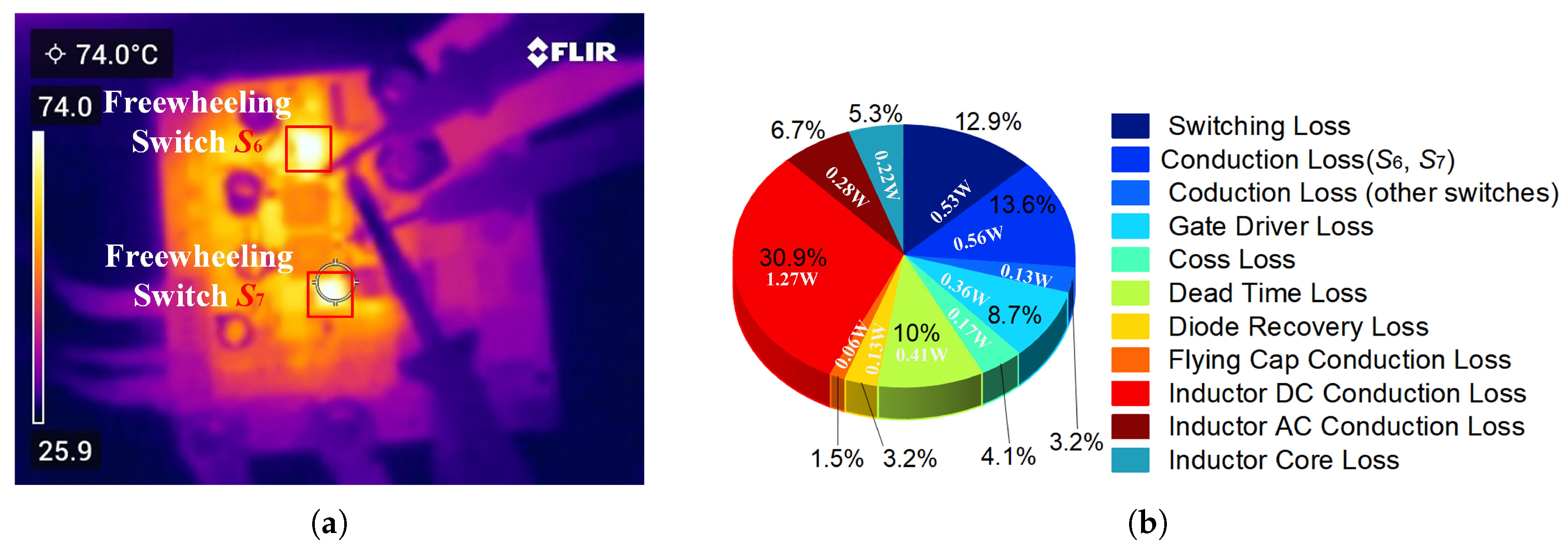
3.2. An Analysis of the Inductor Loss

Inductor losses primarily consist of DC loss, AC loss, and core loss. The average inductor currents I L 1 and I L 2 can be derived from Table 1. Thus, the inductor DC losses before and after duty cycle matching can, respectively, be expressed as
P L , D C , u n m a t c h e d = N 2 N 1 2 + N 1 2 N 1 2 I O 2 R L , D C ,
P L , D C , m a t c h e d = I O 2 2 R L , D C + I O 2 2 R L , D C = 1 2 I O 2 R L , D C ,
where R L , D C is the DC equivalent resistance (DCR) of the inductor, which can easily be obtained from the datasheet.
The AC loss of an inductor is proportional to its current ripple. According to the definition of the RMS value for a periodic waveform (a triangular wave current), the AC RMS current of the inductors can be calculated using calculus as
I L , A C , r m s = Δ I L 2 3 ,
where Δ I L is the inductor current ripple. Combining the ripples Δ I L 1 and Δ I L 2 from Table 1 with Equation (19), the inductor’s AC losses before and after duty cycle matching can, respectively, be signified by
P L , A C , u n m a t c h e d = 1 2 N 1 M 2 6 V O 2 T S 2 R L , A C L 2 ,
P L , A C , m a t c h e d = 1 2 N 1 M 2 + 1 2 N M 2 12 V O 2 T S 2 R L , A C L 2 ,
where R L , A C represents the winding AC resistance, and L denotes the inductance of L 1 and L 2 . Several methods for calculating this resistance are detailed in [31]. However, the necessary parameters are not supplied by the device manufacturers, making it difficult to directly quantify the AC loss.
In the typical 48 V-to-1 V conversion application (M = 1/48), by comparing Equations (17) and (18) as well as (20) and (21), the trends in the inductor’s DC and AC losses before and after duty cycle matching can be determined, as shown in Figure 6. As the order N decreases, the optimization effect of inductor current equalization on the DC loss becomes more apparent. For five- and six-order converters, the reduction in the DC loss can reach 1.22% and 0.82%, respectively. Figure 6 also shows that the increase in the AC loss after duty cycle matching for the six-order converter is only about 0.073%, which can be ignored. Theoretically, the core loss can be calculated using Steinmetz’s formula. However, inductor manufacturers often do not provide parameters for the magnetic core material. Taking IHLP-3232DZ-01 0.47 µH as an example, the inductor losses of a six-order QCSC-TLAHD converter with 48 V to 1 V, I O = 30 A, and a 300 kHz frequency are calculated using VISHAY’s calculation tool [32]. The results are shown in Table 2: the core and AC losses each increase by 1 mW, while the DC loss decreases by 12 mW, leading to a total loss reduction of 10 mW.
Although duty cycle matching makes a limited contribution to overall efficiency improvements, it balances the losses between L 1 and L 2 through inter-inductor loss transfer, which is beneficial for a unified magnetic component selection. Furthermore, it helps equalize the temperature rise of the interleaved inductors.

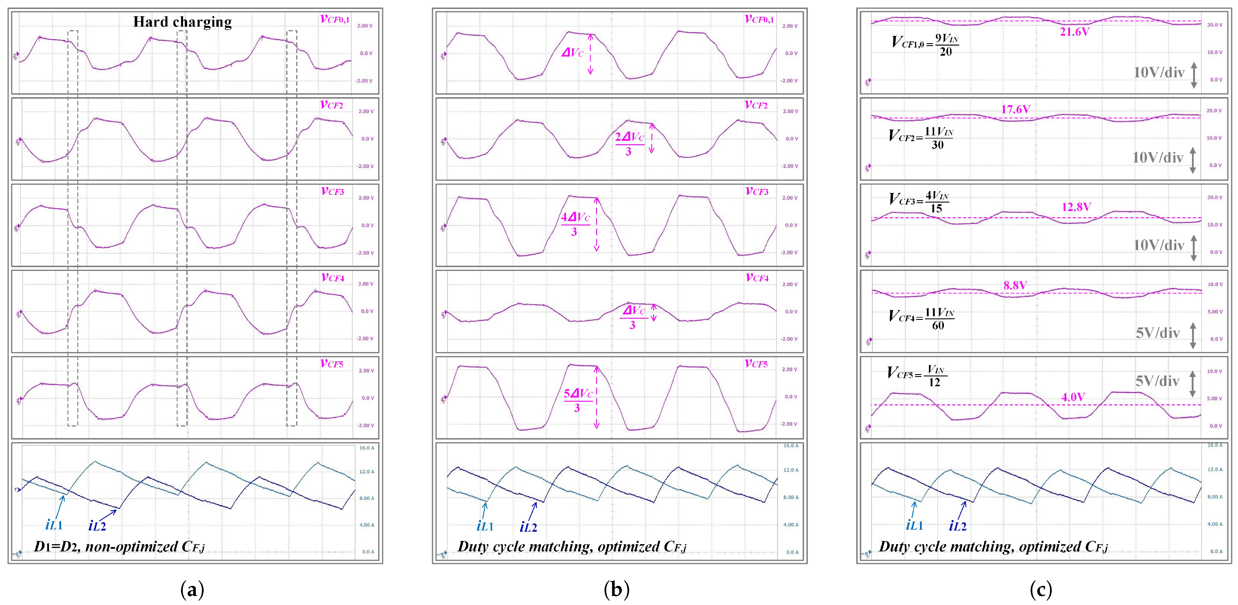
4. Quasi-Complete Soft Charging of Flying Capacitors

Figure 3 illustrates the charging and discharging processes of the flying capacitors in the proposed six-order QCSC-TLAHD converter. In phases Φ 1 and Φ 3 , two distinct capacitor networks are alternately established. During the reconfiguration of capacitor networks, voltage differences among parallel branches cause transient surge currents through low-impedance paths. This leads to short-term hard charging and discharging of the capacitors, which dissipates additional energy in the charge transfer paths, thereby reducing the conversion efficiency. Achieving complete soft charging for all flying capacitors helps eliminate burst currents, thus removing the portion of output impedance known as the slow switch limit (SSL) [33,34]. This not only avoids the need to deliberately increase the capacitance or raise the operating frequency to reduce the equivalent output impedance but also allows for larger voltage ripples across the capacitors, thereby improving their utilization.

4.1. Intrinsic Charge-Ratio-Based Capacitance Optimization

To achieve complete soft charging of the capacitors, an intrinsic charge-ratio-based capacitance optimization method is proposed. The intrinsic charge ratio, determined by the topology and independent of capacitance, refers to the proportion of the charge dynamically transferred across each flying capacitor. This approach necessitates that each flying capacitor transfers charge in accordance with the intrinsic charge ratio during Φ 1 and Φ 3 , while ensuring uniform variation in the voltage across all capacitor branches. This prevents scenarios in which the capacitors either transfer excessive or insufficient charge. If not, dynamic charge rebalancing must occur during capacitor network reconfiguration, resulting in transient surge currents.
In Figure 3a, during Φ 1 , the transferred charges for C F 0 C F 5 are q, q, 2 q , 2 q , 2 q , and 2 q , respectively. In Figure 3b, during Φ 3 , the charges are q , q , 2 q , 2 q , 2 q , and 2 q . Here, the positive and negative signs indicate the accumulation and release of charges in the flying capacitors. Thus, the intrinsic charge ratio for C F 0 C F 5 is (1: 1: 2: 2: 2: 2). During Φ 1 , three parallel capacitor branches ( C F 0 C F 1 , C F 2 C F 3 , and C F 4 C F 5 ) collectively supply charge to L 2 . As shown in Figure 3a, relative to node SW2, the voltage changes across the branches are q C F 0 + q C F 1 , 2 q C F 2 + 2 q C F 3 , and 2 q C F 4 + 2 q C F 5 . If Equation (22) holds, each flying capacitor will transfer charge according to the intrinsic ratio during Φ 1 , resulting in identical voltage variations across each branch.
q C F 0 + q C F 1 = 2 q C F 2 + 2 q C F 3 = 2 q C F 4 + 2 q C F 5
Conversely, if (22) is not met, for instance, when q C F 0 + q C F 1 = 2 q C F 2 + 2 q C F 3 < 2 q C F 4 + 2 q C F 5 , the charge transferred by the branch ( C F 4 C F 5 ) will be less than 2 q during Φ 1 due to the same voltage variation across the parallel capacitor branches. The untransferred portion of the charge in C F 4 and C F 5 will rapidly move in the next operating phase, Φ 3 . Rearranging Equation (22) yields
C F 0 C F 1 C F 0 + C F 1 = 1 2 C F 2 C F 3 C F 2 + C F 3 = 1 2 C F 4 C F 5 C F 4 + C F 5 .
As shown in Figure 3b, during Φ 3 , each of the three capacitor branches transfers a charge of 2 q . Similarly, when (24) is met, the charge of all flying capacitors can be transferred in accordance with the ratio, avoiding sharp currents caused by charge redistribution at the start of Φ 1 . Thus, all flying capacitors charge and discharge softly.
C F 0 + C F 1 C F 2 C F 0 + C F 1 + C F 2 = C F 3 C F 4 C F 3 + C F 4 = C F 5
Additionally, C F 0 and C F 1 operate in series during phase Φ 1 and in parallel during Φ 3 . In Φ 1 , if C F 0 C F 1 , adding the same amount of charge to each will result in different voltage increments. Upon transitioning to the parallel state in Φ 3 , a surge current will occur due to the voltage difference between C F 0 and C F 1 . Thus, it is necessary for C F 0 to equal C F 1 . Assume the capacitance value of C F 0 and C F 1 is C, expressed as
C F 0 = C F 1 = C .
By combining Equations (23), (24), and (25), the optimized values of the flying capacitors can be derived as
C F 0 = C F 1 = C C F 2 = 3 C C F 3 = 1.5 C C F 4 = 6 C C F 5 = 1.2 C .
According to (26), the capacitance values in the six-order QCSC-TLAHD converter can be optimized to theoretically achieve complete soft charging of all capacitors. However, in practical applications, typical deviations and the discrete nature of the capacitance values make achieving the theoretical capacitance ratio challenging. Additionally, factors such as the switch on-resistance and the capacitor ESR further complicate the attainment of complete soft charging for the flying capacitors. Nevertheless, effective reductions in the burst currents can be achieved when the capacitance ratio approximately matches that in (26), facilitating quasi-complete soft charging. It is evident that throughout the entire derivation process of (22)–(26), the duty cycles D 1 and D 2 are not involved. This is because they do not alter the intrinsic charge ratio of the flying capacitors. Therefore, both before and after duty cycle matching, the converter remains suitable for the derivation process, enabling quasi-complete soft charging of the flying capacitors.
Assume
Δ V C = q C .
According to Equations (26) and (27), the voltage ripples of C F 0 C F 5 are Δ V C , Δ V C , 2 3 Δ V C , 4 3 Δ V C , 1 3 Δ V C , and 5 3 Δ V C under quasi-complete soft charging operations, as shown in Figure 3d. The average voltages across the flying capacitors can be obtained from Table 1, and then Table 3 presents the flying capacitor voltages and node voltages.
Figure 7 illustrates the simulated waveforms of the flying capacitor voltages v C F , j ( t ) , currents i C F , j ( t ) , and node voltages v S W 1 , 2 ( t ) for a converter operating with 48 V to 1 V, a 30 A output current, and a 300 kHz switching frequency. In Figure 7a, D 1 equals D 2 , and the capacitance of all of the flying capacitors is 2 µF. In Figure 7b, duty cycle matching is performed, and the optimized values of C F 0 C F 5 are 1 µF, 1 µF, 3 µF, 1.5 µF, 6 µF, and 1.2 µF, respectively. As shown in Figure 7, the simulations reveal that the surge currents are significantly reduced following capacitance optimization. Specifically, before optimization, the surge currents could reach approximately 170 A, whereas after optimization, they consistently remained below 20 A. This substantial reduction in the surge currents indicates that the flying capacitors have entered a quasi-complete soft charging state, thereby minimizing the losses caused by the charge redistribution during switching transitions. This optimization contributes to improving the conversion efficiency. Figure 7a demonstrates that without capacitance optimization, abrupt changes in voltage occur for the flying capacitors during switch transitions, leading to spike currents and resulting in hard charging of the capacitors. Figure 7b shows that after capacitance optimization, quasi-complete soft charging of the flying capacitors can be achieved.

4.2. Capacitance Optimization for N-Order QCSC-TLAHD Converters

The intrinsic charge-ratio-based optimization method for flying capacitors can be extended to N-order QCSC-TLAHD converters. Due to the distinct switched capacitor networks and charge transfer paths in even- and odd-order converters, separate discussions are necessary.
In even-order converters, the flying capacitors, except for C F 0 and C F 1 , which transfer a charge of q, are responsible for a charge transfer of 2 q , with N 2 parallel capacitor branches during phases Φ 1 and Φ 3 . Similar to (23) and (24), to achieve complete soft charging of the flying capacitors C F 0 - C F , N 1 in N-order converters, Equation (28) must be satisfied.
C F 0 C F 1 C F 0 + C F 1 = 1 2 C F 2 C F 3 C F 2 + C F 3 = . . . = 1 2 C F , N 2 C F , N 1 C F , N 2 + C F , N 1 C F 0 + C F 1 C F 2 C F 0 + C F 1 + C F 2 = C F 3 C F 4 C F 3 + C F 4 = . . . = C F , N 3 C F , N 2 C F , N 3 + C F , N 2 = C F , N 1
Substituting (25) into (28) yields the optimized capacitance for flying capacitors as
C F , j | N = E v e n = 2 N N j C , j = 2 , 4 , . . . N 2 2 N N + j 1 C , j = 3 , 5 , . . . N 1 .
In odd-order converters, C F 0 and C F 1 transfer a charge of q, while other capacitors are responsible for a charge transfer of 2 q . Different from even-order converters, odd-order ones have N + 1 2 and N 1 2 parallel capacitor branches during phases Φ 1 and Φ 3 , respectively. To achieve complete soft charging of the flying capacitors, Equation (26) must be met.
C F 0 C F 1 C F 0 + C F 1 = 1 2 C F 2 C F 3 C F 2 + C F 3 = . . . = 1 2 C F , N 3 C F , N 2 C F , N 3 + C F , N 2 = C F , N 1 2 C F 0 + C F 1 C F 2 C F 0 + C F 1 + C F 2 = C F 3 C F 4 C F 3 + C F 4 = . . . = C F , N 2 C F , N 1 C F , N 2 + C F , N 1
Substituting (25) into (30) yields the capacitance as
C F , j | N = O d d = 2 N 1 N + j 1 C , j = 2 , 4 , . . . N 1 2 N 1 N j C , j = 3 , 5 , . . . N 2 .
As derived in (29) and (31), it is evident that both even- and odd-order ( N > 2 ) converters have optimal capacitance solutions for quasi-complete soft charging of the flying capacitors.

4.3. Considerations

Achieving quasi-complete soft charging of flying capacitors can enhance their utilization, allowing them to withstand higher voltage ripples. However, in practical applications, factors such as the switching frequency, input and output voltages, and power transmission must be considered to set the appropriate boundary conditions for the capacitors, ensuring the converter’s normal operation.
At a specific operating frequency, as the power rises, the charge q from V I N during Φ 1 escalates, resulting in higher voltage ripples on the flying capacitors. This directly steepens the switch node voltages v S W 1 , 2 , with the minimum values approaching zero, as shown in the simulation results in Figure 7b. When v S W 2 during Φ 1 or v S W 1 during Φ 3 reaches zero, the inductor current flows through the body diode of the corresponding freewheeling switch, assuming a negligible drop in voltage across the diode. This indicates that the flying capacitors have reached their maximum charge transfer capacity, and the converter has achieved peak power transmission.
In even-order converters, as shown in Table 1, the average voltages V C F , j across flying capacitors after equalization of the inductor current are described as
V C F , j | N = E v e n = 1 4 + N 2 4 N 1 V I N , j = 0 N j + 1 4 N + N j 1 4 N 1 V I N , j = 1 , 3 , 5 , . . . N 1 N j 4 N + N j 4 N 1 V I N , j = 2 , 4 , . . . N 2 .
Equation (25) indicates that the capacitance value of C F 0 and C F 1 is C. During Φ 1 , combining (27), the charge q flows through the capacitor branch C F 0 C F 1 , resulting in a voltage increase of q C C 2 2 ( = 2 Δ V C ). Therefore, the minimum voltage V S W 2 , M I N at node SW2 can be expressed as
V S W 2 , M I N = V I N V C F 0 V C F 1 Δ V C = V I N 2 N 1 Δ V C .
According to (29), the optimized value of C F 2 is denoted as 2 N N 2 C . The equivalent capacitance of the branch ( ( C F 0 C F 1 ) C F 2 ) is represented by N N 1 C during Φ 3 . With the charge of 2 q passing through this branch, a voltage increment 2 N 1 N Δ V C is produced. Integrating this with the average voltages of C F 1 and C F 2 from (32), the minimum voltage V S W 1 , M I N at node SW1 can be described as
V S W 1 , M I N = V C F , 1 V C F , 2 N 1 N Δ V C = V I N 2 N N 1 N Δ V C .
From the analysis above, it is evident that both V S W 1 , M I N and V S W 2 , M I N should be greater than zero to ensure the converter possesses a sufficient energy conversion capability. Thus, from (33) and (34), it is derived as
Δ V C < V I N 2 N 1 .
Under ideal conditions, the converter’s peak power P M A X can be represented as
P M A X = V I N q T S .
Combining Equations (27), (35), and (36), it can be deduced that C > 2 N 1 P M A X T S V I N 2 . Considering the input voltage fluctuates, it must be ensured that
C | N = E v e n > 2 N 1 P M A X T S V I N , M I N 2 ,
where V I N , M I N denotes the minimum input voltage.
For odd-order converters, the derivation follows the same procedure as (32)–(37). The capacitance C must satisfy the constraint given by (34).
C | N = O d d > 2 N P M A X T S V I N , M I N 2

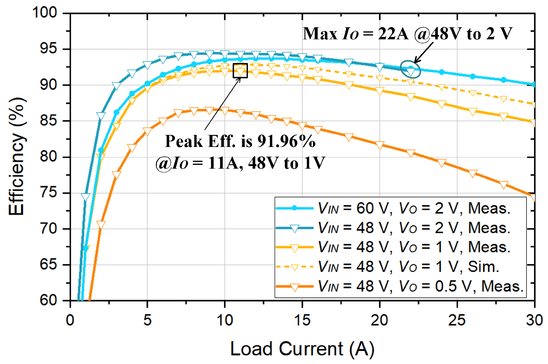
5. The Prototype and Experimental Verification

To verify the feasibility of the proposed topology, a prototype of the six-order QCSC-TLAHD converter was implemented to convert 48 V into 0.5–2.0 V. The prototype and experimental platform are illustrated in Figure 8a and Figure 8b, respectively. To validate the principle of duty cycle matching to equalize the average inductor current, it is essential to flexibly control the ratio of D 1 and D 2 and generate high-frequency drive pulses. In this study, the TMS320F28335PGFA microcontroller from Texas Instruments, featuring high-precision PWM, serves as the controller. Table 1 specifies the ratio of D 1 to D 2 as 6:5. To achieve quasi-complete soft charging, the capacitance optimization is guided by (26), while the selection of the capacitors for other-order converters can be determined using (25), (29), and (31). The list of key components is presented in Table 4.
Figure 9 illustrates that the converter can achieve equalized average inductor currents across various voltage conversion ratios and load conditions. This confirms the effectiveness of the duty-cycle-matching-based current equalization method discussed in Section 3.1. After duty cycle matching, the average currents of inductors L 1 and L 2 are approximately equal, and the slope of i L 2 is greater than that of i L 1 , consistent with the simulation results in Figure 5b. This phenomenon arises from the fact that, after duty cycle matching, inductor L 2 experiences a higher excitation voltage ( V S W 2 > V S W 1 ). This observation aligns with the expressions for the node voltage swings provided in Table 1 for even-order converters.
Figure 10 presents the voltage waveforms of the flying capacitors C F 0 C F 5 and the current waveforms of the inductors L 1 and L 2 during the conversion from 48 V into 1 V with an output current of 20 A in the converter. Without capacitance optimization for C F 0 C F 5 (each being 4 × 0.47 µF, 11.28 µF in total), the voltage ripples are depicted in Figure 10a. The voltage transients in the dashed box indicate hard charging of the flying capacitors. From Figure 10b, the optimized flying capacitors, as listed in Table 4, achieve quasi-complete soft charging. The voltage ripple ratios of C F 0 C F 5 are consistent with those in Figure 3d and Table 3. In addition, the flying capacitors can withstand larger voltage ripples, enhancing their utilization. Figure 10c shows that in steady-state operation, the average voltages of C F 0 C F 5 are approximately 21.6 V, 21.6 V, 17.6 V, 12.8 V, 8.8 V, and 4 V, respectively. These data are consistent with the theoretical values in Table 1 ( 9 V I N 20 , 9 V I N 20 , 11 V I N 30 , 4 V I N 15 , 11 V I N 60 , V I N 12 ), indicating self-balancing of the flying capacitors. The theoretical analysis of voltage balancing in the flying capacitor in Section 2.2 confirms that the balancing is not sensitive to specific capacitor values. The use of low-ESR C0G capacitors minimizes the impact of ESR, ensuring that voltage balancing remains unaffected. During dead time, all power switches are turned off, preventing any influence on the capacitor voltage balancing. Additionally, temperature variations have a negligible effect on the capacitors’ stability, as the C0G capacitors feature a low temperature coefficient, ensuring their stable performance across a wide temperature range.
Figure 11 shows that under specific operating frequency and input–output voltage conditions, as the power consumption increases, the minimum values of the node voltage swings V S W 1 and V S W 2 progressively reduce towards zero. As discussed in Section 4.3, when the minimum values approach zero, the converter reaches its maximum power conversion capacity.
Under natural convection, temperature measurements are taken using an infrared thermometer for the converter operating at 300 kHz with 48 V to 1 V and an output current of 30 A. Figure 12a indicates that the highest temperature in the measured area is approximately 74.0 °C. Two distinct hotspots are observed at the positions of the freewheeling switches S 6 and S 7 , which carry a significantly higher current than all other power switches, as shown in Figure 12b. The power loss breakdown of the converter is shown in Figure 12b. The power switch losses, including the conduction loss, switching loss, and drive loss, can be analyzed according to the method outlined in [35]. The calculation method for ESR loss in flying capacitors is provided in [36]. Inductor-related losses can be calculated using the integrated power inductor calculation tool offered by VISHAY [32]. To ensure the safe operation of the power switches and minimize conduction losses in the body diode, a dead time of 50 ns is implemented. The gate drivers are powered by a 15 V auxiliary supply, which guarantees reliable conduction of the high-side switches (accounting for the drop in voltage of the bootstrap diode) and ensures the low-side switches operate within their specified voltage range. The loss analysis reveals that freewheeling switches S 6 and S 7 contribute approximately 13.6% of the total loss, making them the most lossy active devices. This also explains why S 6 and S 7 become hotspots in Figure 12a. Additionally, the inductors’ losses are the largest, accounting for approximately 42.9%, making them a key focus for improving the conversion efficiency.
Figure 13 depicts the measured efficiency curves of the converter, which converts from 48 V to 1 V, at different operating frequencies after duty cycle matching and capacitance optimization. As the frequency decreases, the conversion efficiency increases. This improvement is primarily attributed to quasi-complete soft charging of the flying capacitors, which facilitates the elimination of SSL resistance. As a result, reducing the frequency does not induce a significant spike current loss and also results in reduced switching losses in the transistors, consequently leading to increased efficiency. However, the decreased frequency results in an extended switching period, as noted in (37), which in turn decreases the converter’s power capacity, leading to a reduction in power density. The prototype discussed in this article operates at a frequency of 300 kHz.
For the converter operating at 300 kHz with a step-down ratio of 48 V to 1 V, Figure 14a presents the measured efficiency curves under three scenarios: (1) duty cycle matching with capacitance optimization; (2) D 1 = D 2 with capacitance optimization; and (3) D 1 = D 2 , C F 0 5 = 4 × 0.47 µF. The results indicate that under a high load current ( I O > 13 A), quasi-complete soft charging of the flying capacitors contributes significantly to efficiency enhancements. Specifically, at a 30 A output, the efficiency demonstrates an improvement of approximately 2.94% after capacitance optimization. Additionally, the measured efficiencies of the converter before and after duty cycle matching are essentially the same, consistent with the analysis in Section 3.2. This indicates that equalizing the average inductor currents has a limited impact on efficiency optimization. Figure 14b shows that at 36 V to 1 V and I O = 22 A, the efficiency optimization reaches up to 5.07%. This phenomenon arises because under the low-input-voltage conditions, the converter operates with a higher duty cycle, necessitating the flying capacitors to transfer more charge for the same output current. Non-optimized flying capacitors experience increased charge transfer during rebalancing, resulting in higher spike current losses. In summary, achieving quasi-complete soft charging of the flying capacitors is crucial for optimizing the converter efficiency.
Figure 15 presents the measured efficiency curves of the converter operating at 300 kHz for various voltage conversions: 60 V to 2 V, 48 V to 2 V, 48 V to 1 V, and 48 V to 0.5 V. Figure 15 also demonstrates that under 48 V-to-1 V conversion, the measured power efficiency of the converter is marginally lower than the simulated values at high-load operation, with this discrepancy predominantly arising from unmodeled parasitic losses in the PCB trace resistance. In the typical 48 V-to-1 V application, the converter achieves a peak efficiency of 91.96% at I O = 11 A. Moreover, the volume of the prototype’s components is quantified as 0.0635 in3. The converter attains a power density of up to 944.88 W/in3.
Table 5 compares the performance of the proposed QCSC-TLAHD converter prototype with several state-of-the-art high-conversion-ratio DC-DC converters. As shown in the table, the QCSC-TLAHD converter achieves the highest duty cycle extension factor ( 2 N 1 ), enabling a higher switch duty cycle, which makes it particularly suitable for high-conversion-ratio step-down applications. The duty cycle extension factor of ( 2 N 1 ), as presented in the third row of Table 5, is derived from (11) and represents the theoretical extension of the duty cycle enabled by the proposed QCSC-TLAHD converter. This factor highlights the converter’s capability to accommodate larger duty cycles, making it particularly advantageous for high-step-down-voltage conversions. The generalized expression in Table 5 facilitates comparison with other topologies, demonstrating that the proposed topology offers a superior duty cycle extension capability. While the peak conversion efficiency of the proposed converter is slightly lower than the 92.4% achieved using the DIH converter in [25], the latter benefits from the use of higher-cost GaN switches. Furthermore, only the volumes of power components such as switches, inductors, capacitors, and drivers are considered in order to compare the volume (power density) performance of the proposed converter with that of other studies. The proposed converter achieves a power density that is second only to that reported in [29]. Although the SDIH converter demonstrates a higher power density, this is achieved at the cost of s significantly lower conversion efficiency. In summary, the comparison in Table 5 highlights that the QCSC-TLAHD converter strikes a favorable balance between power density and conversion efficiency.

6. Conclusions

This article presents a quasi-complete soft charging three-level-assisted hybrid Dickson converter topology suitable for high-step-down-ratio applications. This topology achieves self-balancing of the flying capacitor voltages and average interleaved inductor currents, with both even- and odd-order ( N > 2 ) converters facilitating a ( 2 N 1 )-fold duty cycle expansion. A duty-cycle-matching-based current equalization approach is proposed to ensure equal average inductor currents. Furthermore, an intrinsic charge-ratio-based capacitance optimization method is introduced, enabling quasi-complete soft charging of all flying capacitors, thereby optimizing the conversion efficiency and enhancing the capacitor utilization. Finally, a prototype capable of supporting up to a 30 A load current validates the converter’s operational principles, with voltage conversion from 48 V down to 0.5–2.0 V. The experimental results confirm the equalization of the average inductor currents and quasi-complete soft charging of all flying capacitors. A 2.94% improvement in the conversion efficiency is observed at 48 V to 1 V and a 30 A load, with the peak efficiency reaching 91.96% at 11 A. The prototype attains a power density of up to 944.88 W/in3. Therefore, this converter is a competitive candidate for PoL regulators in large-ratio voltage conversion applications, such as data centers.

Author Contributions

Conceptualization; writing—original draft preparation; software; validation: R.C. Methodology: C.Z. Resources: J.J.L. Formal analysis; project administration; resources; data curation: Y.W. All authors have read and agreed to the published version of the manuscript.

Funding

This research was funded by the Science and Technology Project of Henan Province under Grant No. 232102211076.

Data Availability Statement

The findings generated in the study are included in this article. Additional data and materials are available from the corresponding author upon reasonable request.

Acknowledgments

The authors gratefully acknowledge the valuable contributions of everyone who supported this research.

Conflicts of Interest

The authors declare no competing financial interests or personal relationships that could have influenced the work reported in this paper.

References

  1. International Energy Agency. Electricity 2024—Analysis and Forecast to 2026. Available online: https://iea.blob.core.windows.net/assets/6b2fd954-2017-408e-bf08-952fdd62118a/Electricity2024-Analysisandforecastto2026.pdf (accessed on 10 March 2025).
  2. Li, X.; Jiang, S. Google 48 V Power Architecture. Available online: https://ieeetv.ieee.org/ieeetv-specials/keytalk-xin-li-and-shuai-jiang-google-48v-power-architecture-apec-2017 (accessed on 10 March 2025).
  3. Folmer, S.; Kosakowski, M.; Stala, R. 48-V Input DC-DC High Step-Down Converter in GaN-Based Design. IEEE Access 2022, 10, 115958–115973. [Google Scholar] [CrossRef]
  4. Rahman, S.; Ayaz, M.A.; Khan, I.A. Review of Non-Isolated DC/DC Converters for Application in Data Center Power Delivery. In Proceedings of the 4th International Conference on Smart Grid and Renewable Energy (SGRE), Doha, Qatar, 8–10 January 2024; pp. 1–6. [Google Scholar]
  5. Khan, I.; Rahman, S.; Ayaz, M.A.; Amir, M.; Shehada, H. Review of Isolated DC-DC Converters for Application in Data Center Power Delivery. IEEE Trans. Ind. Appl. 2024, 60, 5436–5446. [Google Scholar] [CrossRef]
  6. Ge, T.; Ye, Z.; Pilawa-Podgurski, R.C.N. A 48-to-12 V Cascaded Multi-Resonant Switched Capacitor Converter with 4700 W/in3 Power Density and 98.9% Efficiency. In Proceedings of the IEEE Energy Conversion Congress and Exposition (ECCE), Vancouver, BC, Canada, 10–14 October 2021; pp. 1959–1965. [Google Scholar]
  7. Ahmed, M.H.; Fei, C.; Lee, F.C.; Li, Q. 48-V Voltage Regulator Module with PCB Winding Matrix Transformer for Future Data Centers. IEEE Trans. Ind. Electron. 2017, 64, 9302–9310. [Google Scholar] [CrossRef]
  8. Ye, Z.; Lei, Y.; Pilawa-Podgurski, R.C.N. The Cascaded Resonant Converter: A Hybrid Switched-Capacitor Topology with High Power Density and Efficiency. IEEE Trans. Power Electron. 2020, 35, 4946–4958. [Google Scholar] [CrossRef]
  9. Ahmed, M.H.; Fei, C.; Lee, F.C.; Li, Q. Single-Stage High-Efficiency 48/1 V Sigma Converter with Integrated Magnetics. IEEE Trans. Ind. Electron. 2020, 67, 192–202. [Google Scholar] [CrossRef]
  10. Ahmed, M.H.; Fei, C.; Lee, F.C.; Li, Q. High-efficiency high-power-density 48/1V sigma converter voltage regulator module. In Proceedings of the IEEE Applied Power Electronics Conference and Exposition (APEC), Tampa, FL, USA, 26–30 March 2017; pp. 2207–2212. [Google Scholar]
  11. Ahmed, M.H.; Fei, C.; Li, V.; Lee, F.C.; Li, Q. Startup and control of high efficiency 48/1V sigma converter. In Proceedings of the IEEE Energy Conversion Congress and Exposition (ECCE), Cincinnati, OH, USA, 1–5 October 2017; pp. 2010–2016. [Google Scholar]
  12. Zou, J.; Brooks, N.C.; Coday, S.; Ellis, N.M.; Pilawa-Podgurski, R.C.N. On the Size and Weight of Passive Components: Scaling Trends for High-Density Power Converter Designs. In Proceedings of the IEEE 23rd Workshop on Control and Modeling for Power Electronics (COMPEL), Tel Aviv, Israel, 20–23 June 2022; pp. 1–7. [Google Scholar]
  13. Pilawa-Podgurski, R.C.; Giuliano, N.D.M.; Perreault, D.J. Merged two-stage power converter architecture with soft charging switched-capacitor energy transfer. In Proceedings of the IEEE Power Electronics Specialists Conference, Rhodes, Greece, 15–19 June 2008; pp. 4008–4015. [Google Scholar]
  14. Ye, Z.; Sanders, S.R.; Pilawa-Podgurski, R.C.N. Modeling and Comparison of Passive Component Volume of Hybrid Resonant Switched-Capacitor Converters. IEEE Trans. Power Electron. 2022, 37, 10903–10919. [Google Scholar] [CrossRef]
  15. Rentmeister, J.S.; Stauth, J.T. A 48V:2V flying capacitor multilevel converter using current-limit control for flying capacitor balance. In Proceedings of the IEEE Applied Power Electronics Conference and Exposition (APEC), Tampa, FL, USA, 26–30 March 2017; pp. 367–372. [Google Scholar]
  16. Liu, X.; Mok, P.K.T.; Jiang, J.; Ki, W.-H. Analysis and Design Considerations of Integrated 3-Level Buck Converters. IEEE Trans. Circuits Syst. I, Reg. Papers. 2016, 63, 671–682. [Google Scholar] [CrossRef]
  17. Das, R.; Le, H.-P. Analysis of Capacitor Voltage Imbalance in Hybrid Converters and Inherently Balanced Operation Using Symmetric Architecture. IEEE J. Emerg. Sel. Top. Ind. Electron. 2022, 3, 1205–1209. [Google Scholar] [CrossRef]
  18. Tanzawa, T. On-Chip High-Voltage Generator: Design Methodology for Charge Pumps; Springer: New York, NY, USA, 2016; Available online: https://link.springer.com/book/10.1007/978-3-319-21975-2 (accessed on 25 March 2025).
  19. Ballo, A.; Grasso, A.D.; Palumbo, G. High-Performance Integrated Charge Pumps: Design and Novel Solutions; Springer: Cham, Switzerland, 2024. [Google Scholar]
  20. Cao, H.; Yang, X.; Xue, C.; He, L.; Tan, Z.; Zha, M. A 12-Level Series-Capacitor 48-1V DC–DC Converter with On-Chip Switch and GaN Hybrid Power Conversion. IEEE J. Solid-State Circuits. 2021, 56, 3628–3638. [Google Scholar] [CrossRef]
  21. Lei, Y.; May, R.; Pilawa-Podgurski, R. Split-Phase Control: Achieving Complete Soft-Charging Operation of a Dickson Switched-Capacitor Converter. IEEE Trans. Power Electron. 2016, 31, 770–782. [Google Scholar] [CrossRef]
  22. Ashourloo, M. Fault Detection in a Hybrid Dickson DC–DC Converter for 48-V Automotive Applications. IEEE Trans. Power Electron. 2021, 36, 4254–4268. [Google Scholar] [CrossRef]
  23. Das, R.; Seo, G.-S.; Le, H.-P. A 120V-to-1.8V 91.5%-Efficient 36-W Dual-Inductor Hybrid Converter with Natural Soft-charging Operations for Direct Extreme Conversion Ratios. In Proceedings of the IEEE Energy Conversion Congress and Exposition (ECCE), Portland, OR, USA, 23–27 September 2018; pp. 1266–1271. [Google Scholar]
  24. Seo, G.-S.; Das, R.; Le, H.-P. Dual Inductor Hybrid Converter for Point-of-Load Voltage Regulator Modules. IEEE Trans. Ind. Appl. 2020, 56, 367–377. [Google Scholar] [CrossRef]
  25. Das, R.; Seo, G.-S.; Le, H.-P. Analysis of Dual-Inductor Hybrid Converters for Extreme Conversion Ratios. IEEE J. Emerg. Sel. Top. Power Electron. 2021, 9, 5249–5260. [Google Scholar] [CrossRef]
  26. Ellis, N.M.; Pilawa-Podgurski, R.C.N. Modified Split-Phase Switching with Improved Fly Capacitor Utilization in a 48V-to-POL Dual Inductor Hybrid-Dickson Converter. In Proceedings of the IEEE Energy Conversion Congress and Exposition (ECCE), Vancouver, BC, Canada, 10–14 October 2021; pp. 1735–1740. [Google Scholar]
  27. Ellis, N.M.; Pilawa-Podgurski, R.C.N. A Symmetric Dual-Inductor Hybrid Dickson Converter for Direct 48V-to-PoL Conversion. In Proceedings of the IEEE Applied Power Electronics Conference and Exposition (APEC), Houston, TX, USA, 20–24 March 2022; pp. 1267–1271. [Google Scholar]
  28. Ellis, N.M.; Sambo, H.; Robert Pilawa-Podgurski, C.N. Closed-Loop Split-Phase Control Applied to the Symmetric Dual Inductor Hybrid (SDIH) Converter. In Proceedings of the IEEE 24th Workshop on Control and Modeling for Power Electronics (COMPEL), Ann Arbor, MI, USA, 25–28 June 2023; pp. 1–6. [Google Scholar]
  29. Ellis, N.M.; Abramson, R.A.; Mahony, R.; Pilawa-Podgurski, R.C.N. The Symmetric Dual Inductor Hybrid Converter for Direct 48V-to-PoL Conversion. IEEE Trans. Power Electron. 2024, 39, 7278–7289. [Google Scholar] [CrossRef]
  30. Baba. Benefits of a Multiphase Buck Converter. Texas Instruments. Available online: https://www.ti.com/lit/an/slyt449/slyt449.pdf (accessed on 12 March 2025).
  31. Reatti, A.; Kazimierczuk, M.K. Comparison of various methods for calculating the AC resistance of inductors. IEEE Trans. Magn. 2002, 38, 1512–1518. [Google Scholar] [CrossRef]
  32. Vishay Dale. IHLP Inductor Core Loss Calculator Tool. Available online: https://www.vishay.com/en/inductors/calculator/calculator/ (accessed on 10 March 2025).
  33. Henriksen, M.M.; Otten, J.; Gehl, A.; Wicht, B. The ΔV-Method: An Intuitive Method for Analyzing Soft-Charging Capabilities of Hybrid Switched-Capacitor DC-DC Converters. In Proceedings of the IEEE 24th Workshop on Control and Modeling for Power Electronics (COMPEL), Ann Arbor, MI, USA, 25–28 June 2023; pp. 1–6. [Google Scholar]
  34. Seeman, M.D.; Sanders, S.R. Analysis and Optimization of Switched-Capacitor DC–DC Converters. IEEE Trans. Power Electron. 2008, 23, 841–851. [Google Scholar] [CrossRef]
  35. Jauregui, D.; Wang, B.; Chen, R. Power Loss Calculation with Common Source Inductance Consideration for Synchronous Buck Converters. Application Report (SLPA009A), Texas Instruments. 2011. Available online: https://www.ti.com/lit/an/slpa009a/slpa009a.pdf (accessed on 10 March 2025).
  36. Chen, C.; Liu, J.; Lee, H. Dual-Path Hybrid Dickson Converter for High-Ratio Conversions in Point-of-Load Applications. IEEE Trans. Ind. Appl. 2023, 59, 6914–6925. [Google Scholar] [CrossRef]
Figure 1. The proposed QCSC-TLAHD topology: (a) even- and (b) odd-order.
Electronics 14 02001 g001
Figure 2. The six-order QCSC-TLAHD converter with optimized capacitor values.
Electronics 14 02001 g002
Figure 3. The equivalent circuits of the QCSC-TLAHD converter during (a) Φ 1 , (b) Φ 3 , and (c) Φ 2 , 4 , alongside (d) ideal operational waveforms.
Electronics 14 02001 g003
Figure 4. Comparison of D-M (duty cycle vs. conversion ratio) across various converter topologies.
Electronics 14 02001 g004
Figure 5. Simulated waveforms of inductor currents i L 1 and i L 2 under (a) D 1 = D 2 and (b) matched D 1 , 2 .
Electronics 14 02001 g005
Figure 6. Trends in inductor DC and AC losses before and after duty cycle matching.
Electronics 14 02001 g006
Figure 7. Simulated waveforms of flying capacitor voltages v C F , j ( t ) , currents i C F , j ( t ) , and node voltages v S W 1 , 2 ( t ) : (a) D 1 = D 2 , (b) duty cycle matching.
Electronics 14 02001 g007
Figure 8. (a) The prototype and (b) experimental platform of the proposed six-order QCSC-TLAHD converter.
Electronics 14 02001 g008
Figure 9. Experimental waveforms of the inductor currents before and after duty cycle matching at an operating frequency of 300 kHz for (a) 36 V-to-1 V, 5 A; (b) 48 V-to-1 V, 15 A; and (c) 60 V-to-1 V, 25 A.
Electronics 14 02001 g009
Figure 10. Experimental waveforms of flying capacitor voltages and inductor currents before and after duty cycle matching at 48 V-to-1 V/20 A and a 300 kHz frequency. (a) D 1 = D 2 , C F 0 5 = 4 × 0.47 µF, (b) duty cycle matching, capacitance optimization (ripple), and (c) duty cycle matching, capacitance optimization (average).
Electronics 14 02001 g010
Figure 11. Operation waveforms of switching nodes as power consumption increases at 48 V-to-1 V/300 kHz.
Electronics 14 02001 g011
Figure 12. (a) Thermal image and (b) power loss breakdown of the prototype operating at 48 V to 1 V, 30 A and 300 kHz.
Electronics 14 02001 g012
Figure 13. Measured power efficiency curves at 48 V-to-1 V across different working frequencies.
Electronics 14 02001 g013
Figure 14. Experimental efficiency improvements following capacitance optimization at (a) 48 V-to-1 V and (b) 36 V-to-1 V.
Electronics 14 02001 g014
Figure 15. Measured and simulated power efficiency curves.
Electronics 14 02001 g015
Table 1. Converter parameters before and after duty cycle matching.
ParameterD1 = D2Duty Cycle Matching
Even-OrderOdd-OrderEven-OrderOdd-Order
D 1 2 N 1 M 2 N M 2 N 1 M
D 2 2 N 1 M 2 N M
V C F , j j = 0 N 1 2 N 1 V I N 1 4 + N 2 4 N 1 V I N 1 4 + N 1 4 N V I N
j = O d d N j 2 N 1 V I N N j + 1 4 N + N j 1 4 N 1 V I N N j 4 N + N j 4 N 1 V I N
j = E v e n N j 4 N + N j 4 N 1 V I N N j + 1 4 N + N j 1 4 N 1 V I N
V S W 1 V I N 2 N 1 V I N 2 N V I N 2 N 1
V S W 2 V I N 2 N 1 V I N 2 N
I L 1 N 2 N 1 I O N 1 2 N 1 I O I O 2
I L 2 N 1 2 N 1 I O N 2 N 1 I O
Δ I L 1 V O 1 2 N 1 M T S L V O 1 2 N M T S L V O 1 2 N 2 M T S L
Δ I L 2 V O 1 2 N 2 M T S L V O 1 2 N M T S L
Table 2. Inductor losses calculation results.
D1 = D2D1,2 Matching
Inductor L 1 L 2 L 1 L 2
Pcore (W)0.1090.1090.1170.102
PDC (W)0.7570.5270.6360.636
PAC (W)0.1370.1370.1450.130
Ptotal (W)1.0030.7730.8980.868
Temp. rise (℃)22.717.520.319.7
Table 3. The flying capacitor voltages v C F , j and node voltages V S W 1 , 2 in the six-order QCSC-TLAHD converter.
PhaseParameterD1 = D2Duty Cycle Matching
InitialFinal Δ InitialFinal Δ
Φ 1 v C F 0 , 1 5 V I N 11 Δ V C 2 5 V I N 11 + Δ V C 2 Δ V C 9 V I N 20 Δ V C 2 9 V I N 20 + Δ V C 2 Δ V C
v C F 2 4 V I N 11 + Δ V C 3 4 V I N 11 Δ V C 3 2 Δ V C 3 11 V I N 30 + Δ V C 3 11 V I N 30 Δ V C 3 2 Δ V C 3
v C F 3 3 V I N 11 2 Δ V C 3 3 V I N 11 + 2 Δ V C 3 4 Δ V C 3 4 V I N 15 2 Δ V C 3 4 V I N 15 + 2 Δ V C 3 4 Δ V C 3
v C F 4 2 V I N 11 + Δ V C 6 4 V I N 11 Δ V C 6 Δ V C 3 11 V I N 60 + Δ V C 6 11 V I N 60 Δ V C 6 Δ V C 3
v C F 5 V I N 11 5 Δ V C 6 V I N 11 + 5 Δ V C 6 5 Δ V C 3 V I N 12 5 Δ V C 6 V I N 12 + 5 Δ V C 6 5 Δ V C 3
V S W 2 V I N 11 + Δ V C V I N 11 Δ V C 2 Δ V C V I N 10 + Δ V C V I N 10 Δ V C 2 Δ V C
Φ 3 v C F 0 , 1 5 V I N 11 + Δ V C 2 5 V I N 11 Δ V C 2 Δ V C 9 V I N 20 + Δ V C 2 9 V I N 20 Δ V C 2 Δ V C
v C F 2 4 V I N 11 Δ V C 3 4 V I N 11 + Δ V C 3 2 Δ V C 3 11 V I N 30 Δ V C 3 11 V I N 30 + Δ V C 3 2 Δ V C 3
v C F 3 3 V I N 11 + 2 Δ V C 3 3 V I N 11 2 Δ V C 3 4 Δ V C 3 4 V I N 15 + 2 Δ V C 3 4 V I N 15 2 Δ V C 3 4 Δ V C 3
v C F 4 2 V I N 11 Δ V C 6 4 V I N 11 + Δ V C 6 Δ V C 3 11 V I N 60 Δ V C 6 11 V I N 60 + Δ V C 6 Δ V C 3
v C F 5 V I N 11 + 5 Δ V C 6 V I N 11 5 Δ V C 6 5 Δ V C 3 V I N 12 + 5 Δ V C 6 V I N 12 5 Δ V C 6 5 Δ V C 3
V S W 1 V I N 11 + 5 Δ V C 6 V I N 11 5 Δ V C 6 5 Δ V C 3 V I N 12 + 5 Δ V C 6 V I N 12 5 Δ V C 6 5 Δ V C 3
Table 4. Key components and parameters.
ComponentDesign Selection
C F 0 C F 5 3 × 0.22 µF, 3 × 0.22 µF, 4 × 0.47 µF/0.1 µF, 2 × 0.47 µF,
8 × 0.47 µF/2 × 0.1 µF, 0.47 µF/0.22 µF/0.1 µF, Murata, C0G
C O 6 × 47 µF, 6.3 V, Murata, X7R
C I N 6 × 10 µF, 100 V, TDK, X7R
S 1 S 5 BSC026NE2LS5, Infineon
S 6 , S 7 BSC009NE2LS5I, Infineon
S 8 BSC066N06NS, Infineon
S 9 S 11 BSC059N04LS6, Infineon
L 1 , L 2 IHLP3232DZERR47M01, VISHAY
MicrocontrollerTMS320F28335PGFA, TI
High-side driver8 × LTC4440-5, ADI
Low-side driver3 × UCC27517DBVR, TI
Table 5. Comparisons among different converters suitable for large-ratio step-down applications.
TPE
2020 [22]
TPE
2023 [29]
JESTPE
2021 [25]
TIA
2023 [36]
ECCE
2021 [26]
This Work
TopologyHDSDIHDIHDPHDDIHQCSC-TLAHD
M ( V O V I N ) 2 D N D N D N 2 D N + 2 D + N 2 (Even)
2 D N + 1 D + N 1 (Odd)
D N D 2 N 1
VIN/VO48 V/3.3V48 V/1–3 V48 V/1–2 V36–65 V/1–2 V48 V/1–3 V48 V/0.5–2 V
Max. IO10.9 A116 A20 A32 A70 A30 A
Type/Num.
of Switches
MOS/32MOS/14GaN/9MOS/10MOS/8MOS/11
fSW250 kHz750 kHz150 kHz250 kHz750 kHz300 kHz
Capacitor12106656
Inductor4 × 3.3 µH2 × 150 nH2 × 2.2 µH260 nH2 × 1 µH2 × 470 nH
Component
Volume (a)
N/A0.073 in3N/A0.135 in30.168 in30.0635 in3
Power Density (a)N/A1588 W/in3N/A481 W/in3892 W/in3944.88 W/in3
Peak
Efficiency
N/A83.5%
@48/1 V
92.4%
@48/1 V
90.6%
@48/1 V, 13 A
87.5%
@48/1 V
91.96%
@48V/1 V, 11 A
(a) Considering only the component volume in the power stage.
Disclaimer/Publisher’s Note: The statements, opinions and data contained in all publications are solely those of the individual author(s) and contributor(s) and not of MDPI and/or the editor(s). MDPI and/or the editor(s) disclaim responsibility for any injury to people or property resulting from any ideas, methods, instructions or products referred to in the content.

