Article

A Generative Model-Based Method for Inverse Design of Microstrip Filters

1
Research Center of Applied Electromagnetics, Nanjing University of Information Science and Technology, Nanjing 210044, China
2
State Key Laboratory of Millimeter Waves, Southeast University, Nanjing 210096, China
*
Author to whom correspondence should be addressed.
Electronics 2025, 14(10), 1989; https://doi.org/10.3390/electronics14101989
Submission received: 10 April 2025 / Revised: 7 May 2025 / Accepted: 9 May 2025 / Published: 13 May 2025

Abstract

:
In the area of microstrip filter design and optimization, deep learning (DL) algorithms have become much more attractive and powerful in recent years. Here, we propose a method to realize the inverse design of passive microstrip filters, applying generative adversarial networks (GANs). The proposed DL-assisted framework is composed of three components, including a compositional pattern-producing network GAN-based graphic generator, a convolution neural network (CNN)-based electromagnetic (EM) response predictor, and a genetic algorithm optimizer. The filter adopts a square patch resonator structure with an irregular-graphic slot and corner-cuts introduced at diagonal positions. By constructing a hybrid model of pixelated patterns in the filter structures and the corresponding EM response S-parameters, we can obtain customized filter solutions with wideband and dual-band magnitude responses in the 3–8 GHz and 1–6 GHz frequency range, respectively. For each inverse design, it cost 3.6 min for executing 1000 iterations, on average. Numerical simulations and experimental results show that the S-parameters of the generated filters are in excellent agreement with the self-defined targets.

1. Introduction

Recently, neural networks (NNs) have been employed to design and optimize microstrip filters. This approach allows for the direct extraction of geometric or physical parameter values from the given electromagnetic (EM) parameter results, offering advantages such as automation in processing and low computational resource consumption [1,2]. Traditionally, commonly used neural network models in the inverse design of EM devices include multilayer perceptron (MLP), convolutional neural networks (CNNs), recurrent neural networks (RNNs), generative neural networks, as well as hybrid models that combine NNs with optimization algorithms.
Over the past few years, the inverse design of EM devices has developed rapidly; in particular, training deep neural networks (DNN) models enables the inverse design of microwave devices [3,4,5,6], nanophotonic devices [7,8], power splitters [9], demultiplexer [10], metamaterial absorbers [11,12], and multifunction metasurfaces [13]. Owing to the ability of learning latent features from datasets and generating new models to tackle the challenge of non-uniqueness, generative models, including generative adversarial networks (GANs) [14] and variational autoencoders (VAEs) [15], have emerged as promising approaches in the EM inverse design field. By learning the latent distribution of dataset features, these networks can generate novel topological structures for devices. In the field of inverse design for metasurfaces, methods based on conditional GANs (CGANs) and Wasserstein GANs (WGANs) were among the first to be proposed, integrating generative models with EM simulators to design metasurface unit cells tailored to specific transmission spectra [16]. Subsequently, a GAN-based method for the inverse design of EM metasurfaces with ultra-wideband anisotropic reflection phase characteristics was developed in the domain of deep learning-assisted electromagnetic metasurface design [17]. To address the challenges posed by strong interlayer coupling effects and the complexity of conventional synthesis methods, a metasurface design method based on a novel scatterer structure was proposed. This approach employed VAE techniques in conjunction with optimization algorithms to effectively solve single- and multi-constraint optimization problems [18]. Furthermore, by integrating VAE networks with equivalent circuit theory, the inverse design of multilayer metasurfaces was achieved [19]. Hybrid generative models that integrate NNs with optimization algorithms have been subsequently proposed for a series of metasurface inverse design studies [20,21,22].
Currently, deep learning-based microstrip filter design primarily focuses on the forward design and optimization of filter parameters [23,24,25,26,27]. According to the principles of NNs, a trained model can be applied to the inverse design of microstrip filters, and several studies have successfully integrated neural network techniques with optimization algorithms to achieve inverse filter design. For the traditional inverse design of microwave filters, there are two types of shallow NN-based methods, including the comprehensive NN [28] and the multivalued NN inverse modeling approach [29]. These methods using integrated inverse sub-models can effectively address the non-uniqueness problem of NN models, achieving the inverse design of a fourth-order dielectric resonator filter and a sixth-order multi-coupled cavity filter [30]. Machine learning techniques have also been successfully employed in the inverse design of microwave photonic filters, where a model was proposed to predict filter design parameters that yield the desired frequency response [31]. Subsequently, a dimensionality reduction strategy based on artificial neural networks (ANNs) was introduced to simplify the inverse modeling process, which was applied to coupling matrix extraction and waveguide filter optimization [32]. To overcome gradient vanishing issues during the neural network training, several researchers have utilized neural network techniques to model and design filters, including high-order multi-coupled cavity filters [33], parameter extraction, and the estimation of microstrip bandpass filters (BPF) [34,35]. Furthermore, a method combining GANs with transfer learning algorithms was proposed and applied to the inverse design of active low-pass filters [36]. Therefore, the utilization of generative models, especially combined with optimization, for designing microstrip filters has significant values.
In this work, a hybrid model integrating GANs with optimization algorithms to achieve the inverse design of passive microstrip filters is proposed. This comprehensive model enables the simultaneous output of multiple pixelated patterns of square patch resonators in the filter structure and corresponding EM data. GAN combined with a genetic algorithm is better suited for addressing complex, highly diverse design problems. Although with higher computational complexity, the robust global search capability can help overcome intricate design challenges.

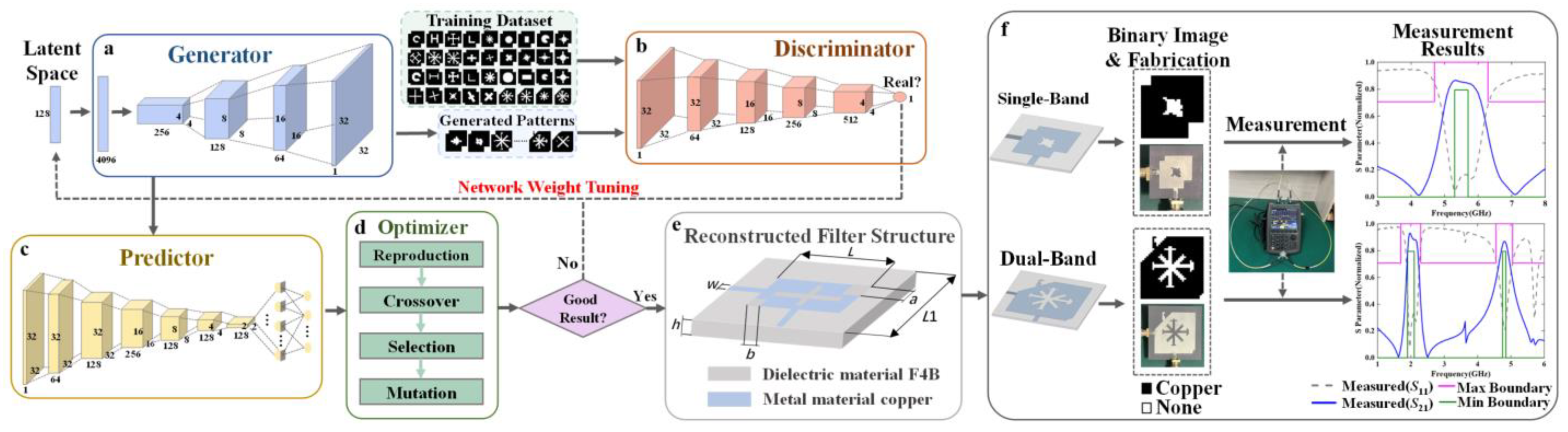
2. Materials and Methods

2.1. Structures of Filters and Training Datasets

The structure of the microstrip filter is depicted in Figure 1e, comprising a single metal layer and a dielectric layer. The substrate is F4B with a thickness of 0.8 mm and a dielectric constant of 2.65. The square patch resonator is chosen as the structure, along with halving the filter order and effectively reducing the filter size. Two types of perturbations, including corner-cut and slots, are employed in the filter modeling: (1) Introducing a square or triangular corner-cut at the diagonal positions of the square patch can result in the disruption of structure symmetry and the separation of degenerate mode resonance frequencies. (2) Shaped slots etching at the center of the square patch alter the effective current loop length of the resonator. Thereby, increasing the length of the slot can decrease the resonant frequency, and a series of filters with different center frequencies are created by using various shaped slots. In addition, in order to effectively mitigate coupling losses and enhance out-of-band performance, two orthogonal feeding lines are directly coupled at the edge of the patch. The training dataset consists of two parts: geometric shapes and corresponding EM simulation data for the filters. Each physical structure of square patch resonator corresponds to a binary pixel image, which is represented as a 32 × 32 matrix. In order to enrich the diversity of the geometric dataset, 20 types of shapes are selected as slot perturbations, including arc, H-shape, L-shape, ellipse, rectangle, sector, cross, dagger, Latin cross, cross with ellipse, cross with rectangle, and various rotated angles, combined with different sizes of angular cuts, totaling 47 geometric shapes. Therefore, a range of bandpass characteristics with varying cutoff frequencies is achieved by altering the patterns. Based on the prototype shown above, simulated transmission coefficients (S21) and reflection coefficients (S11) of filter models are automatically constructed in ANSYS HFSS 2019 with the aid of MATLAB R2022b. The geometric training dataset consists of 12,590 samples. The detailed information of the geometric training datasets is presented in Supplementary File S1.

2.2. Inverse Design Process

The overall framework and process of the deep learning approach based on GAN networks is illustrated in Figure 1. It includes a generator, a discriminator, an electromagnetic response predictor based on convolutional neural networks (CNNs), and a genetic algorithm optimizer. The generator and discriminator form the compositional pattern-producing network (CPPN) GAN network as follows: the generator is trained to generate shapes resembling those in the geometric training dataset, while the discriminator is utilized to distinguish between generated fake patterns and real images. The training process minimizes the distance between the distributions of these two datasets by iteratively updating the generator’s weights. The predictor network takes 32 × 32 pixelated geometric patterns as input and predicts the EM parameters (S11 and S21) corresponding to the filters. This network establishes a mapping between the physical structure of the filter and its EM characteristics. The genetic algorithm optimizer is responsible for selecting better-performing structures, updating and feeding these latent vectors back into the generator to improve geometric patterns. Through multiple iterations targeting the response, the optimal pattern is chosen as the resonator metal layer structure for the filter, and an inverse design yields a binary matrix corresponding to this structure which can be fabricated and measured.

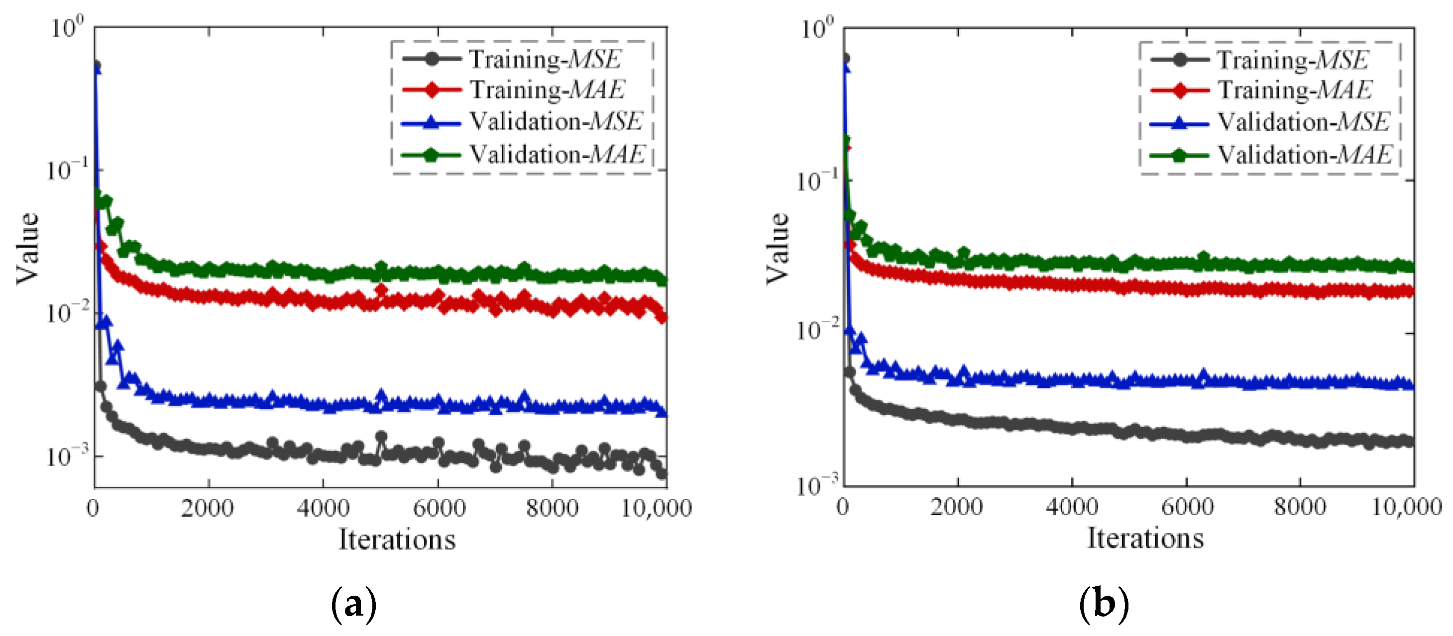
2.3. Neural Network Architecture

The detailed NN architectures of the generator, the discriminator, and the predictor are illustrated in Figure 1a–c. All the tensors are depicted as colored blocks in the figure, with the sized labelled at the bottom of each block. The generator consists of one linear layer and three transpose convolutional operation (Conv2DTranspose) layers with “ReLU” and “Sigmoid” activation function. The total 128-point random data form the input vector in the latent space, and the generator transforms the input latent vector into a composite image with 32 × 32 pixels. On the contrary, the input of the discriminator is represented as a tensor with the dimension of (32, 32, 1). After four stepwise convolution operations (Conv2D) and “ReLU” activation function, the tensor is transformed to the 1 dimension to output a binary classification decision (true/fake). The output of the discriminator is utilized to measure the Euclidean distance between the distribution of the generated patterns and the geometric dataset.
To efficiently calculate the performance of filters, a predictor that can approximate the transmission/reflection coefficients without using EM simulations needs to be developed. Due to the excellent performance of adjusting network depth according to the task requirements and the dataset size, the ResNet18 model is chosen to build the EM predictor. ResNet18 is particularly well suited for learning the complex spatial relationships between the geometric images of microstrip filters and their corresponding S-parameters, and its residual connections help alleviate the vanishing gradient problem, enabling a balance between model complexity and computational efficiency. The predictor takes one 32 × 32 pixel pattern as input and outputs the coefficients within the target frequency range. Thus, normalized S21 and S11 within 0 to 1 are all sampled at 64 points and the output dimension is 2 × 64 = 128. The detailed structures and configurations of the proposed neural network model are shown in Supplementary File S2.
The proposed CPPN-GAN was trained with the following optimized hyperparameters. The batch size was set to 64, the dimension of the latent vector was set to 128, and the learning rates of both the discriminator and generator were set to 0.00005. Adam was employed as the optimizer, with the discriminator trained for five iterations per generator iteration. The total number of training iterations was set to 40,000. The training results are presented in Supplementary Material Figure S3.
Here, in order to improve the training accuracy, two predictors are separately introduced in the proposed inverse design for the single-band and dual-band filter models, which are simulated and trained within the frequency ranges of 3–8 GHz and 1–6 GHz, respectively. To validate the predictor’s accuracy, evaluation metrics including mean squared error (MSE) and mean absolute error (MAE) are used, and they are expressed as (1) and (2), as follows:
M S E = 1 n i = 1 n T goal f i T predicted f i 2
M A E = 1 n i = 1 n T goal f i T predicted f i
Here, Tgoal and Tpredicted represent the target coefficients and the predicted value, and fi represents the i-th frequency data point.
75% of the database was randomly selected as the training set for predictor training, with the remaining 25% used as the test set. Figure 2a,b display MSE and MAE curves during predictor training for the single-band and dual-band filter. After 10,000 training iterations, the average MSE and MAE of the single-band predictor converged to less than 0.0007 and 0.009, respectively. Validation results on the test set demonstrate that the predictor is capable of estimating the S-parameters corresponding to each geometric structure in the single-band filter test set with an average MAE of less than 0.016. Similarly, the dual-band predictor converged to average MSE and MAE values below 0.0018 and 0.018, respectively, and demonstrated an average MAE below 0.026 on the corresponding test set. It demonstrates good agreement between predicted and simulated results.
Figure 3a,b provide examples of predictors for single-band and dual-band filters; pixelated images in insets are corresponding to the filters, red and blue circles depict predicted normalized S-parameters, and solid lines represent actual simulated values of the filters. It demonstrates good agreement between predicted and simulated results.

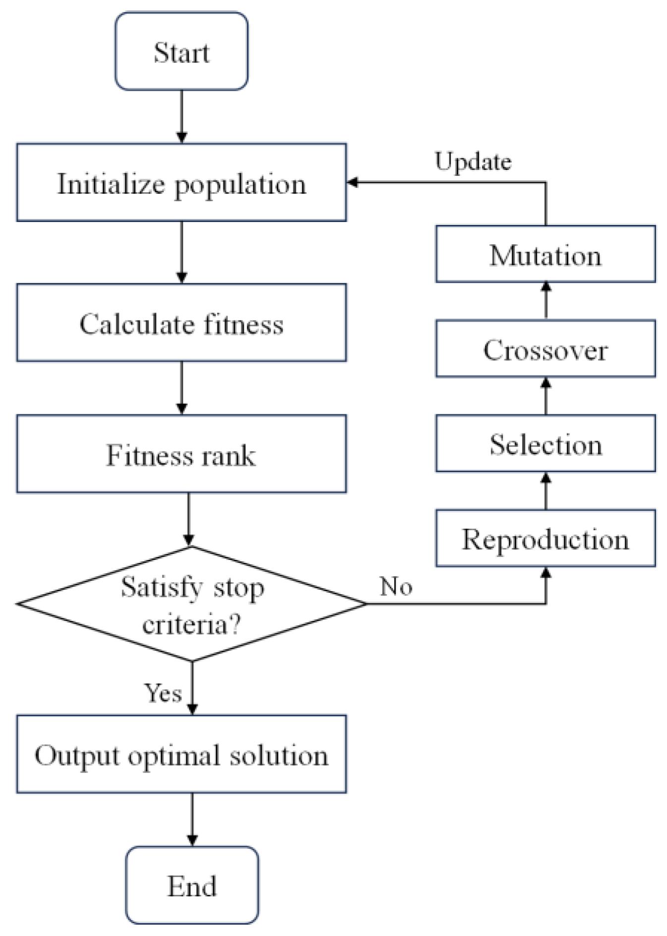
2.4. Genetic Algorithm Optimizer

As illustrated in Figure 4, the implementation of a genetic algorithm (GA) typically includes steps such as encoding, initial population generation, fitness function computation, selection, crossover, mutation, and termination condition evaluation. This study adopts real-valued encoding, and maps geometric shapes corresponding to filters onto a 128-dimensional latent vector, encoding each image directly with 128 real numbers. The initial population is generated by randomly producing a specified number of initial solutions. The fitness function evaluates the fitness or quality of each individual. By progressively eliminating individuals with lower fitness values and promoting those with higher fitness values through multiple generations of evolution, the algorithm ultimately converges to the solution with the highest fitness value, representing the optimal solution to the problem. Selection is based on the magnitude of fitness function values to determine which individuals proceed to the next generation, while crossover and mutation operations generate new individuals. The detailed information of the GA optimizer is given in Supplementary File S3.

3. Results and Analysis

To validate the effectiveness of the proposed method, testing was conducted using customized maximum and minimum boundaries as inputs, achieving bandwidth transformations. All the codes were implemented in PyCharm 2023.3.2. The key third-party library versions used are as follows: PyTorch 1.2.0, Keras 2.3.1, TensorFlow 2.2.0, NumPy 1.16.0, and Matplotlib 3.3.0, with the development environment being PyCharm IDE. The implementation, training, and execution of deep learning models were implemented on a workstation equipped with an NVIDIA GeForce GTX 2080Ti GPU, Intel Xeon E5-4210v2 @ 2.2 GHz CPU, and 128GB of memory. During a complete inverse design process, executing 1000 iterations on the GPU workstation averaged 3.6 min.

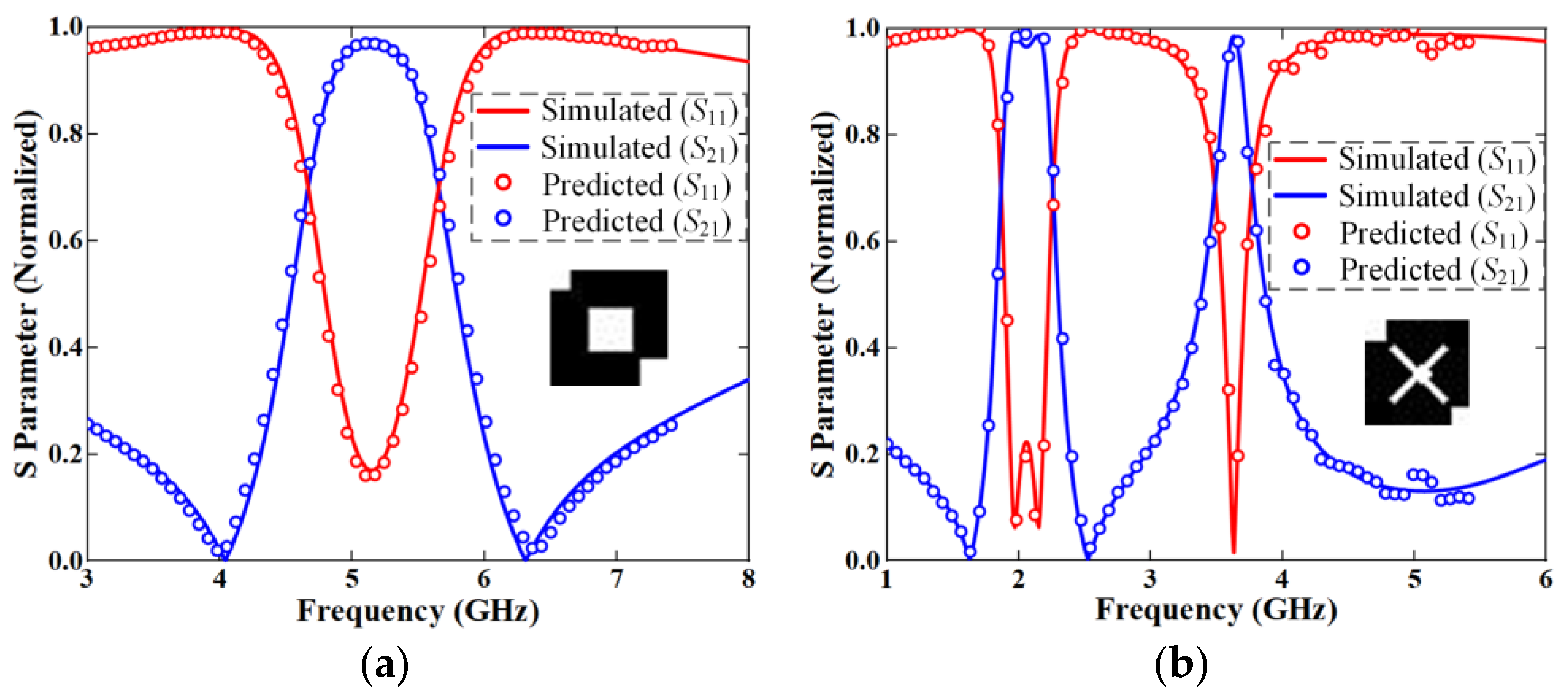
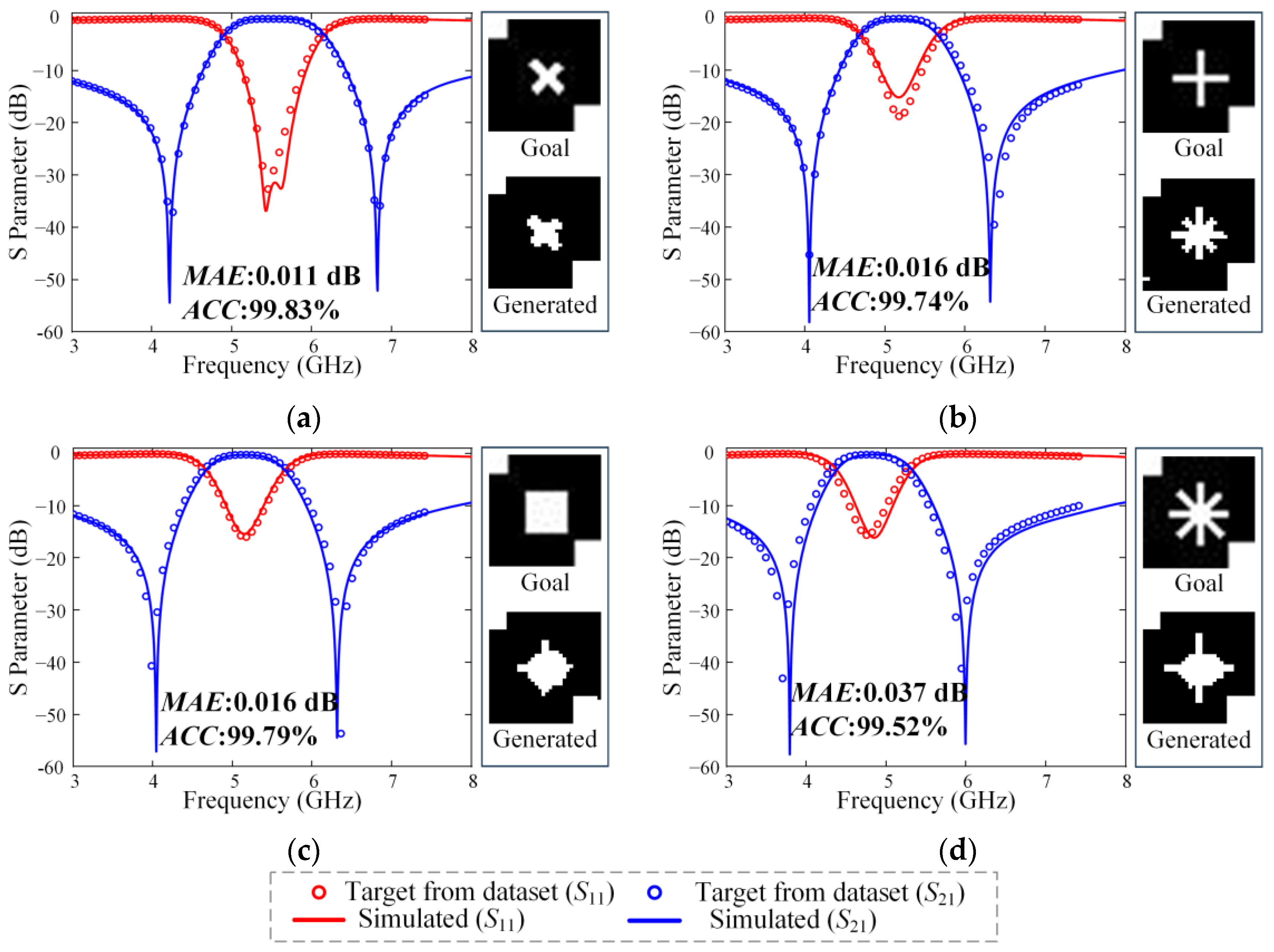
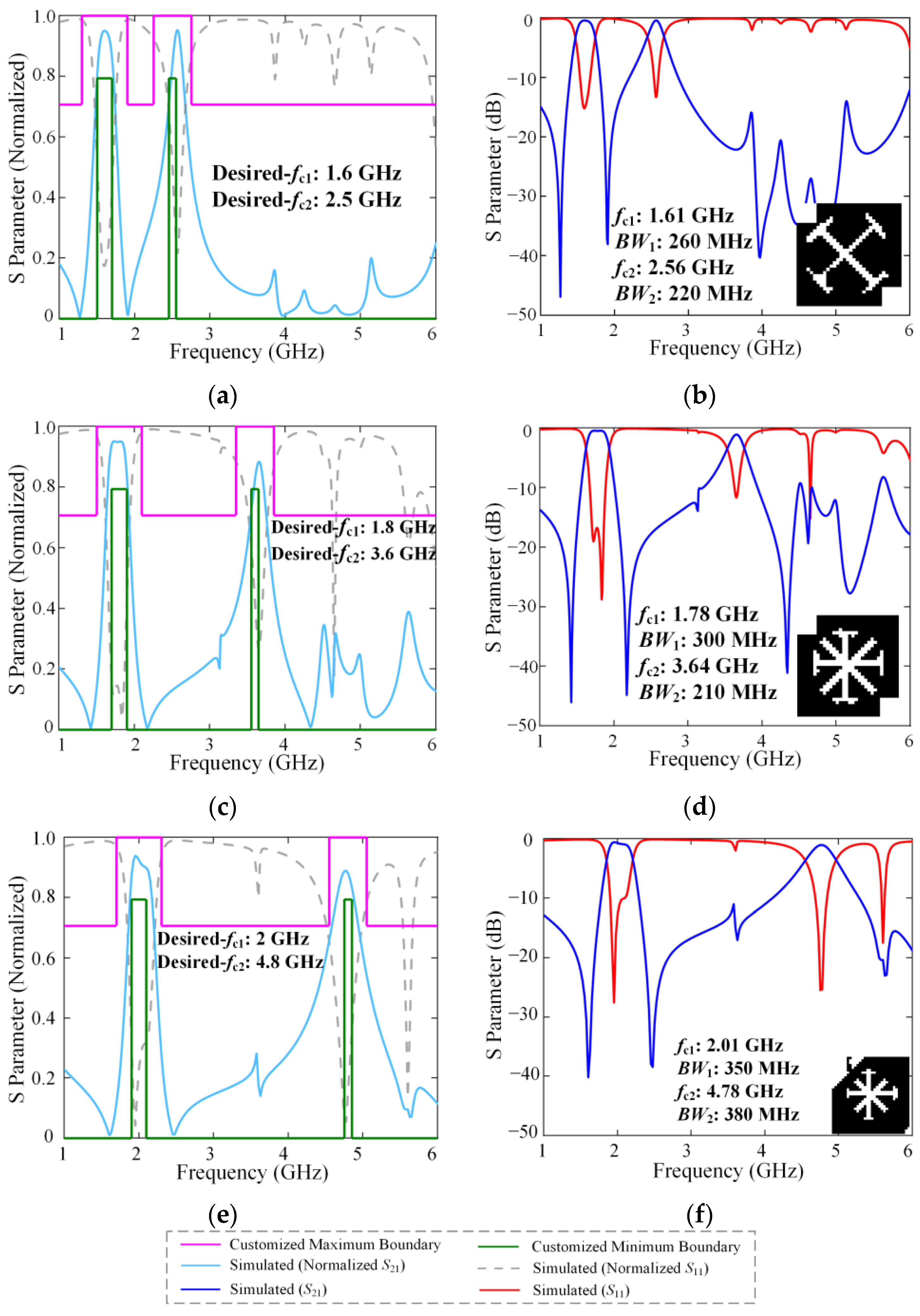
3.1. Inverse Design Test Under the Target Curve of Dataset

In this study, different loss functions were designed for inverse design tasks based on dataset targets and self-defined targets, respectively. For the dataset target curves, the chosen loss function is the L2 norm between the target S-parameters and the S-parameters generated by the inverse design, representing the Euclidean distance between the distributions of the two datasets, defined as follows:
L 2 = | | T goal T generated | | 2 = i = 1 n ( T goal ( f i ) T generated ( f i ) ) 2 n
Here, n denotes the total size of the transmission coefficient data points, Tgoal and Tgenerated represent the target and simulated values, respectively, and fi represents the i-th frequency data point.
To quantitatively evaluate the accuracy of the inverse design results based on the target curves in the dataset, two assessment metrics were introduced: the mean absolute error (MAE) and average accuracy (ACC). These metrics systematically measure the degree of agreement between the target curves and the curves generated through inverse design. ACC is defined as follows:
A C C = 1 1 n i = 1 n | T g o a l   ( f i ) T g e n e r a t e d   ( f i ) |
Figure 5 and Figure 6 illustrate comparisons between four single-band and four dual-band target curves and their inverse-designed results, respectively.
The inverse design model takes the target curve from EM parameter datasets. The target is defined as 128 data points: the first 64 points are sampled from the S11 curve and the latter 64 points are extracted from S21 values, corresponding to red and blue circles in Figure 5 and Figure 6. Each example presents the patterns corresponding to the target curve as well as the actual generated pattern. EM simulations of these models yield the generated filter’s return loss and insertion loss, represented by solid red and blue lines in Figure 5 and Figure 6.
Through inverse design based on database target curves for both single-band and dual-band filters, followed by comprehensive accuracy and reliability analysis, the simulation demonstrates that while discrepancies exist between the target patterns and the inverse designed patterns, excellent consistency is observed between the target S-parameters and the simulated S-parameters of the inverse designed filters. Furthermore, within the passband, the reflection and insertion losses satisfy the conditions of |S11| > 10 dB and |S21| < 3 dB. For the single-band, the average MAE and average ACC were 0.019 dB and 99.72%, respectively. For the dual-band, the corresponding values were 0.035 dB and 99.47%. These results verify that the proposed inverse design method offers high accuracy and can effectively facilitate the design of passive filters.
Some additional samples of single-band and dual-band filters selected from different geometric classes compared with the simulated results are presented in Supplementary Files S4 and S5, respectively.

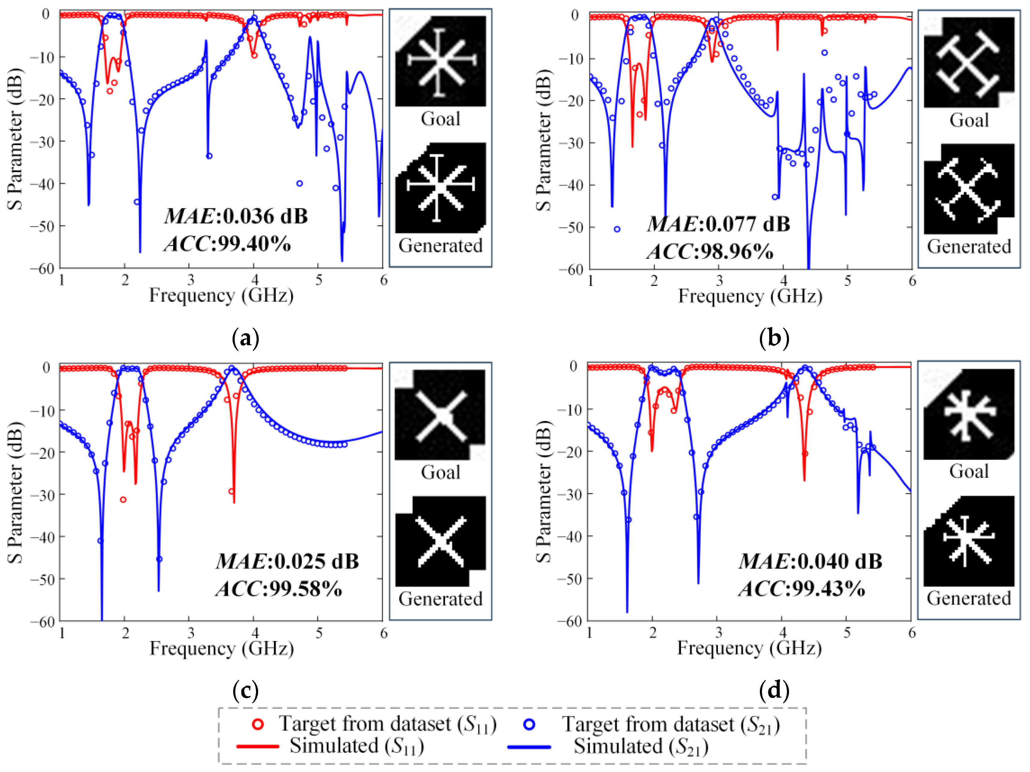
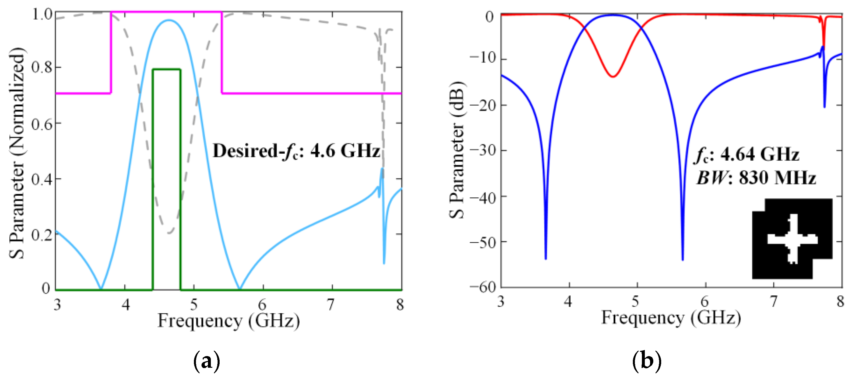
3.2. Inverse Design Test Under the Self-Defined Target Curve

For the customized target curve, the entire frequency band of the filter is divided into several sub-bands, each with self-designed thresholds for S11 and S21, which are then used to construct an appropriate loss function. As shown in (5), the loss function L comprises the S11 loss LS11 and S21 loss LS21, where γ is a scaling factor adjusting the loss function according to different design objectives.
L = γ × L S 11 + ( 1 γ ) × L S 21
L S 11 = ( S 11 S 11 min ) ( S 11 S 11 max ) T + ( S 11 S 11 min ) ( S 11 S 11 max ) T
L S 21 = ( S 21 S 21 min ) ( S 21 S 21 max ) T + S 21 S 21 min S 21 S 21 max T
Here, S11min and S21min are the minimum desired values for S11 and S21, while S11max and S21max denote the maximum desired values.
The proposed integrated model is employed for the inverse design of single-band and dual-band filters under the self-defined target. The input of the model consists of customized maximum and minimum boundaries for S11 and S21, and it carries out the inverse design and iterative optimization process by incorporating loss functions (5), (6), and (7). The generator produces the pixelated patterns, which are then fed into the predictor to output the S-parameters. Finally, combined with the GA optimization algorithm, the optimal pixelated pattern is obtained.
To quantitatively evaluate the accuracy of the inverse design results based on customized target curves, the selected evaluation metric is the error between the desired center frequency (desired-fc) and the actual center frequency (fc), where a smaller value indicates higher accuracy of the inverse design. Additionally, the S-parameter curves generated through inverse design must lie within the self-defined maximum and minimum threshold curves.
Using the developed inverse design model, three examples and corresponding simulated S-parameters of single-band filters are provided in Figure 7, and the final generated patterns are also shown in the inset of each figure. The tunable range for the fc of the single-band filter spans from 4.6 GHz to 5.4 GHz, with the minimum and maximum 3 dB target bandwidth (BW) set to 400 MHz (green line) and 1.6 GHz (pink line), respectively. The simulation results demonstrate that the range of each filter meets the specified requirements, indicating the feasibility of the proposed method. Some additional samples of inverse design test of single-band filters under the self-defined objective are given in Supplementary File S6. It can be observed that the center frequency of the single-band filter is adjusted within the range of 4.6 GHz to 5.5 GHz. A statistical analysis of the customized inverse design results for the single-band filter shows that the average error between the desired- fc and the actual fc is 0.05 GHz.
Figure 8 shows the inverse design-generated patterns of three dual-band filters and corresponding simulated S-parameters. The range for the low-passband center frequency (fc1) is adjusted from 1.6 GHz to 2 GHz, with the minimum and maximum 3 dB bandwidths (BW1) set to 200 MHz and 500 MHz, respectively. The high-passband center frequency (fc2) tuning range spans from 2.5 GHz to 4.8 GHz, with the minimum and maximum 3 dB bandwidths (BW2) set to 100 MHz and 400 MHz, respectively. Some additional examples of inverse design tests of dual-band filters under the self-defined objective are shown in Supplementary File S7. The bandwidth of two passbands can be independently controlled: With fc1 fixed at 1.6 GHz, the fc2 is independently tunable within the range of 2.5 GHz to 4.2 GHz. Similarly, when the fc1 remains constant at 1.8 GHz, the fc2 can be varied from 2.8 GHz to 4.6 GHz. Lastly, with the fc1 held steady at 2 GHz, the fc2 is adjustable within the range of 3.4 GHz to 4.8 GHz. A statistical analysis of the customized inverse design results for the dual-band filter indicates that the average error between the desired and actual fc1 is 0.04 GHz, while the average error between the desired and actual fc2 is 0.05 GHz.

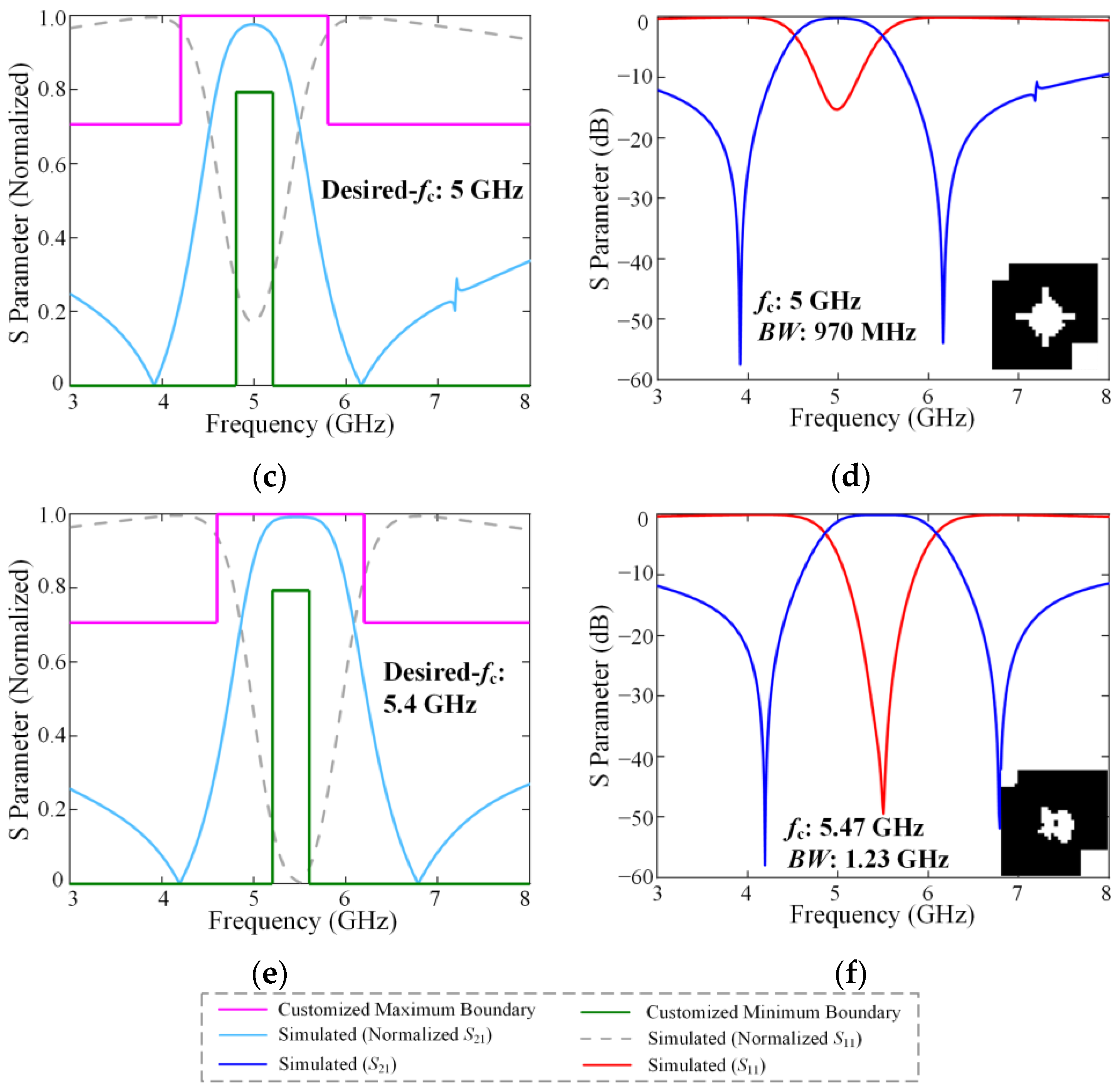
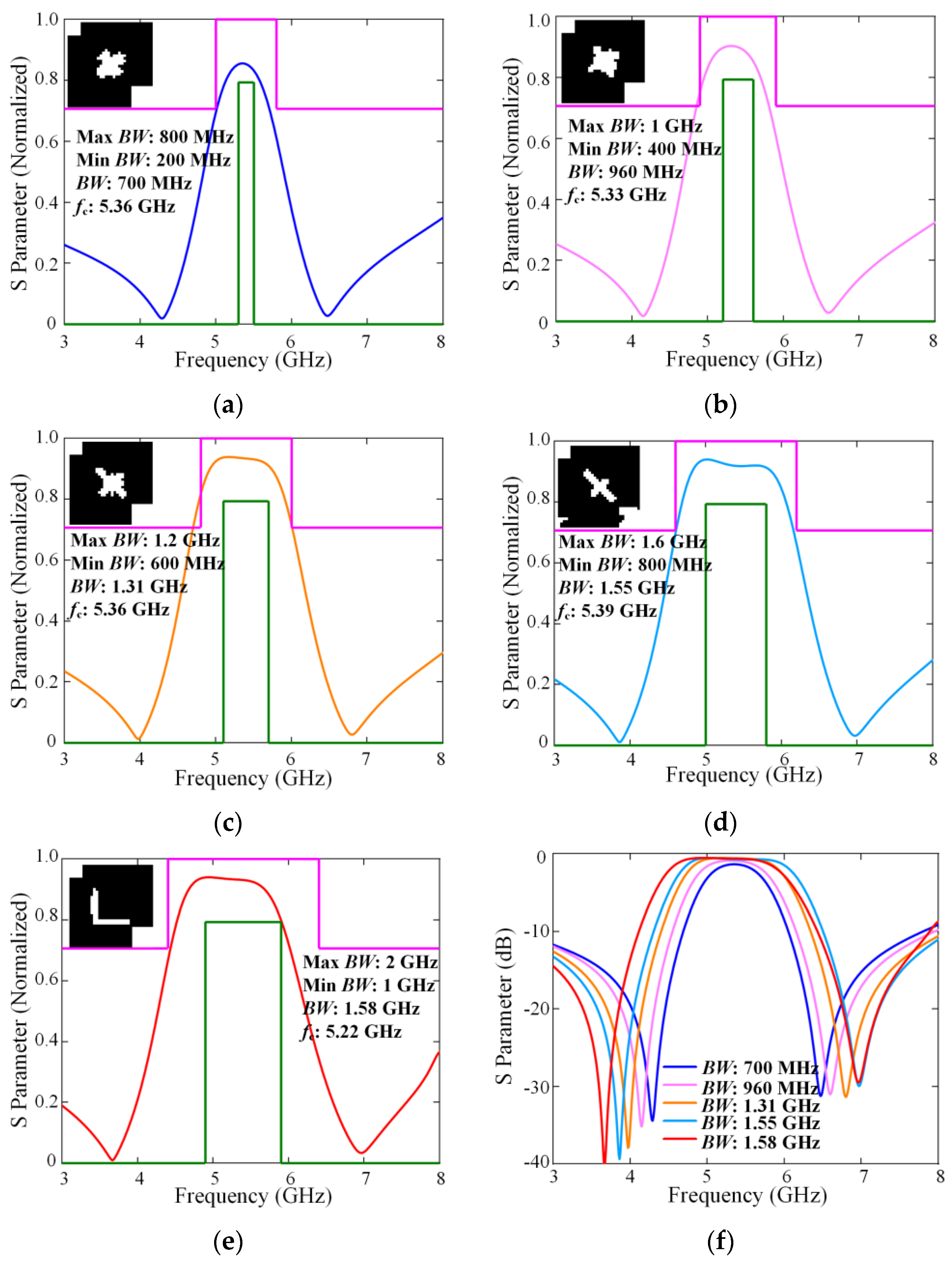
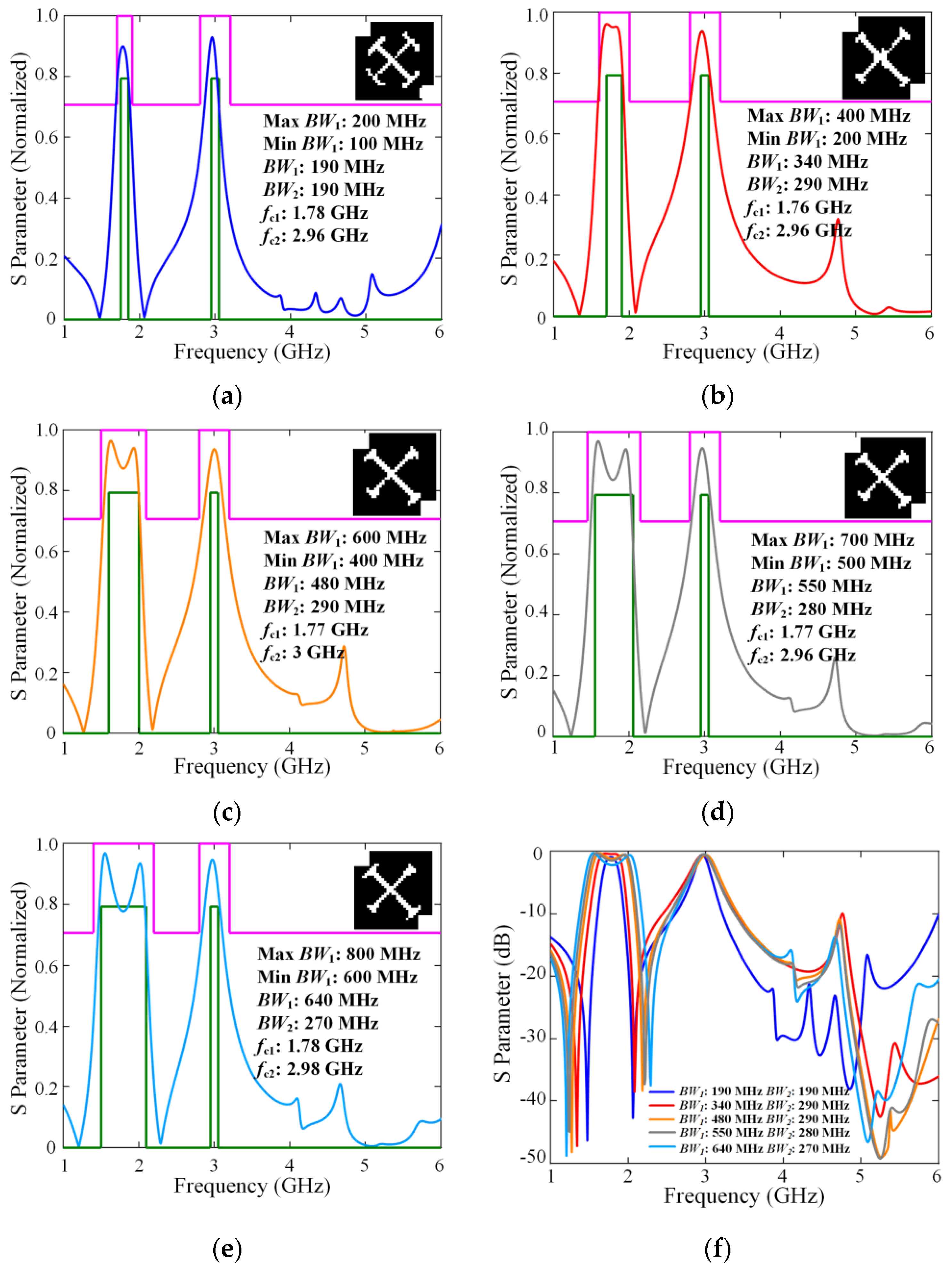
3.3. Inverse Design Test Under the Bandwidth-Transformations Target Response

For single-band filters, a specific fc is chosen, and then the bandwidth boundaries of the target curves are sequentially increased based on the fc. Figure 9a–e illustrates the customized design process with fc maintained at 5.4 GHz, depicting variations in maximum and minimum bandwidths. The generated patterns are illustrated in insets, accompanied with the normalized S21 curves from EM simulations depicted in the figures. Figure 9f presents the overall result of bandwidth scaling transformations. When fc is kept approximately constant at 5.4 GHz, the 3 dB bandwidth can be increased from 700 MHz to 1.58 GHz.
Figure 10a–e illustrate a self-defined inverse design process where the center frequencies of the low-pass and high-pass bands are kept constant at fc1 = 1.8 GHz and fc2 = 3 GHz, respectively. Figure 10f shows the overall result of the bandwidth scaling transformation. With the low-passband fc1 fixed at 1.8 GHz, the 3 dB bandwidth (BW1) can be varied from 190 MHz to 640 MHz. While with the high-passband fc2 fixed at 3 GHz, the 3 dB bandwidth (BW2) shows a slight variation, ranging from 190 MHz to 290 MHz.

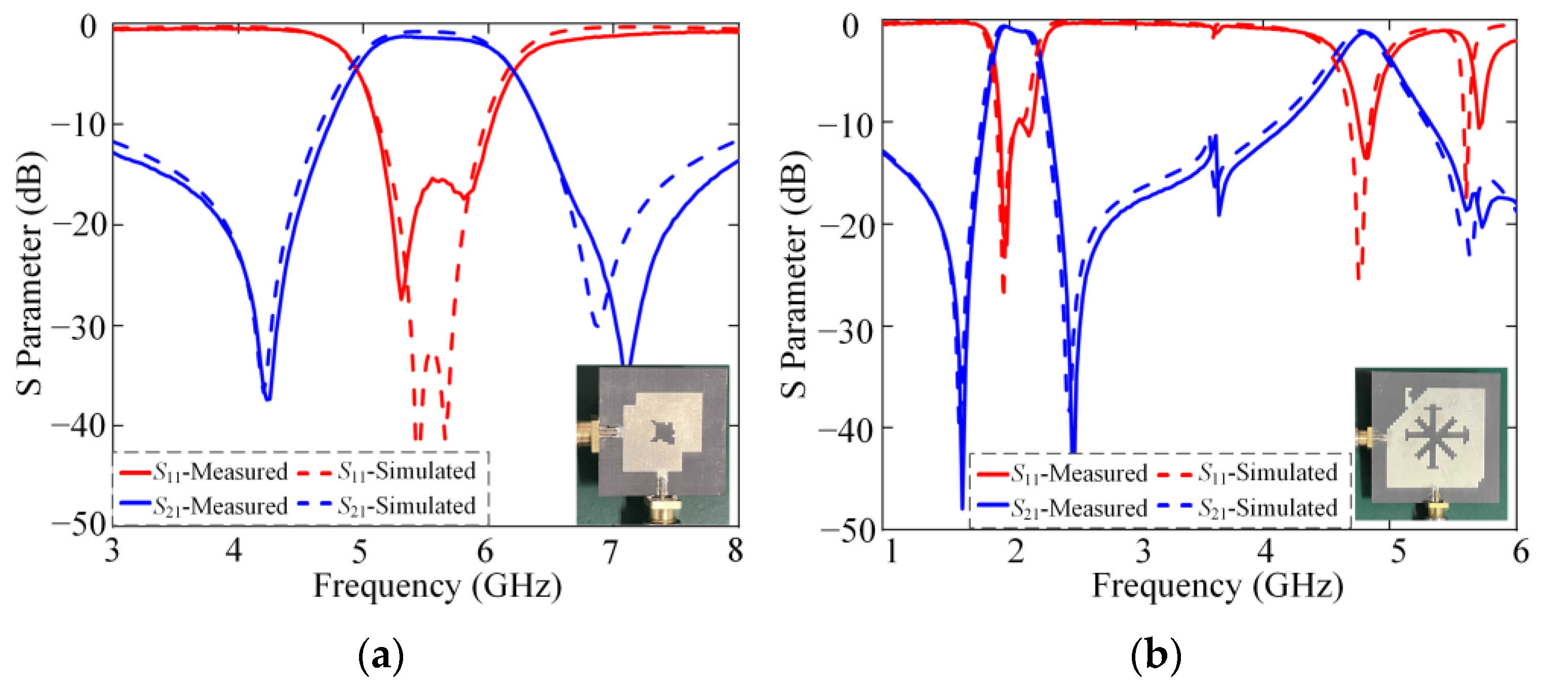
4. Fabrication and Measurement

To validate the accuracy of the proposed inverse design methodology, both a single-band and a dual-band filter prototype were fabricated and experimentally characterized. The two prototypes were fabricated on an F4B substrate, possessing a thickness of 0.8 mm. The results of both simulations and measurements are illustrated in Figure 11. The wideband filter has dimensions of 26 × 26 mm2, with a measured frequency range of 3–8 GHz, while the dual-band filter measures 42 × 42 mm2, with a measured frequency range of 1–6 GHz.
For the wideband filter in Figure 11a, the measured insertion loss within the passband is less than 1.23 dB, and the measured return loss is greater than 15.3 dB, with two transmission zeros located on each side of the passband. The measured center frequency is 5.56 GHz with a 3 dB bandwidth of 1.06 GHz, while the simulated center frequency is 5.53 GHz with a 3 dB bandwidth of 1.12 GHz.
For the dual-band filter in Figure 11b, the measured return losses within the two passbands are both larger than 10.8 dB. The measured insertion loss within the two passbands is less than 1.19 dB. The measured center frequency of the lower passband is 2.05 GHz with a 3 dB bandwidth of 360 MHz, while the simulated center frequency is 2.03 GHz with a 3 dB bandwidth of 340 MHz. For the upper passband, the measured center frequency is 4.8 GHz with a 3 dB bandwidth of 320 MHz, and the simulated center frequency is 4.77 GHz with a 3 dB bandwidth of 360 MHz. In addition, there are transmission zeros on both sides of the passband, demonstrating good out-of-band suppression performance.
The slight discrepancies between the measured and simulated results may be attributed to fabrication tolerances and process artifacts. In future work, additional simulation studies involving variations in the length, width, and geometry of the microstrip lines can be conducted to further enhance the model robustness. The detailed information of the fabrication and measurement is presented in Supplementary File S8.
To rigorously evaluate the performance of the proposed CPPN-GAN-based inverse design methodology, comparative experiments were conducted against the state-of-the-art conditional deep convolutional generative adversarial network (CDCGAN) approach. The CDCGAN employs a CNN-based generator to directly synthesize complete images in a single forward pass. In contrast, the CPPN-GAN utilizes a CPPN as its generator, which adopts a point-wise mapping strategy. Specifically, the CPPN takes the coordinates of each pixel as input, predicts the corresponding pixel value through iterative computation, and finally assembles all predicted pixels to construct the complete image. Unlike CDCGAN, which uses a traditional random vector as input, our model leverages a spatially structured latent space generated by CPPN, which better captures geometric patterns in microstrip structures. For both models, the batch size was set to 64, and the learning rates for the generator and discriminator were set to 0.00005. Both inverse design models were fed with identical target response curves from the database, with comprehensive performance metric comparisons of the inverse design results systematically presented in Table 1.
Furthermore, a comparison of other key technical properties of the designed filters with those recently reported methods is shown in Table 2.

5. Discussion

The CPPN-GAN architecture employed in this study demonstrates significant advantages over conventional approaches. In the proposed framework, the CPPN functions as the generator within the GAN structure. As an innovative generative framework, CPPN-GAN effectively integrates CPPN with GAN, leveraging the structural capabilities of CPPN to generate intricate patterns while employing the adversarial training mechanism of GANs to produce complex and diverse images. The CPPN network takes a bias vector v and the spatial coordinates (x,y,r) as input, where the bias vector governs the global geometric features of the generated pattern, and r denotes the normalized distance from pixel (x,y) to the center of the image. In the CPPN-based generator, each neuron layer is associated with a bias vector, which shifts the output of the activation function, thereby forming a nonlinear mapping from spatial coordinates to pixel intensities in the generated structure.
During adversarial training, the bias vectors are treated as trainable parameters and iteratively optimized through backpropagation using gradients from the discriminator. The discriminator evaluates the realism and performance relevance of the generated filter structures based on their predicted S-parameters. Through this process, the generator learns to produce microstrip layouts whose EM responses increasingly resemble the target frequency responses. This coordination between the CPPN and the discriminator ensures that the generator not only captures the geometric patterns of feasible filter designs but also aligns them with the functional requirements.
Unlike traditional CNNs that directly output entire images, CPPN adopts a point-wise mapping strategy by taking pixel coordinates as input to predict their corresponding pixel values. Once all pixel coordinates are iteratively processed, the predicted values are assembled into a complete image. Due to this pixel-wise generation mechanism, the trained CPPN can flexibly produce patterns with arbitrarily complex geometric features, such as corner-cut and slots. These features are critical for realizing bandpass filters, highlighting the significant potential of CPPN in exploring novel resonator structures. Moreover, when trained on graphical datasets with specific geometric characteristics, CPPN can stochastically generate a diverse set of patterns, offering a powerful tool for various inverse design tasks.
As evidenced by the comparative results presented in Table 1, the proposed CPPN-GAN with GA method outperforms the existing CDCGAN. Under the same experimental conditions and dataset size, the CDCGAN-based inverse design method requires approximately 12.5 min on average to complete 20,000 iterations for each target. In contrast, the proposed method achieves the same convergence criteria with only 1000 iterations per target, taking approximately 3.6 min, thus significantly reducing the time cost. Simulation results demonstrate that the proposed method outperforms existing approaches in terms of ACC, MAE, and MSE, confirming its superiority in design accuracy.
The comparison results in Table 2 indicate that the filters obtained through inverse design using the proposed method exhibit superior performance. The proposed method is capable of designing both single-band and dual-band filters, demonstrating broader applicability. Through structural optimization, the method effectively reduces the filter order and simplifies the design complexity, while exhibiting superior performance in key metrics such as in-band return loss and fractional bandwidth.

6. Conclusions

In this study, we present a hybrid model combing GANs with a genetic algorithm optimizer for the inverse design of passive microstrip filters. Through analyzing the tunability of center frequencies and bandwidths within the passbands, this study focuses on customized objective function inverse design for single-band and dual-band filters in the frequency range of 3–8 GHz and 1–6 GHz, respectively. Both a single-band and a dual-band filter model were selected for fabrication and testing. The single-band filter demonstrated measured insertion loss below 1.23 dB and return loss exceeding 15.3 dB. The dual-band filter showed measured insertion losses below 1.19 dB within both passbands, with return losses exceeding 10.1 dB. Transmission zeros were observed on both sides of the passbands for both single-band and dual-band filters, indicating that filters designed using the inverse design method proposed in this study exhibit effective out-of-band suppression performance. This work provides a smart way to automatically design microstrip filters with a fast speed and low computational resource consumption. In the future, the architecture of generative neural networks can be further optimized, for example by incorporating VAEs, to improve the accuracy of inverse design. Additionally, more advanced optimization algorithms, such as reinforcement learning and meta-learning, can be introduced to enhance the stability of network training. Furthermore, the application scope can be expanded by exploring broader use cases of generative neural network techniques in microwave device design.

Supplementary Materials

The following supporting information can be downloaded at https://www.mdpi.com/article/10.3390/electronics14101989/s1: It mainly contains detailed information of datasets, neural network, optimization algorithm, and additional examples of inverse design test of single-band and dual-band filters. S1. Detailed information of the geometric training datasets; S2. Detailed information of the network architecture; S3. Detailed information of the genetic algorithm optimizer; S4. Additional samples of inverse design test of single-band filters under the target curves in the dataset; S5. Additional samples of inverse design test of dual-band filters under the target curves in the dataset; S6. Additional samples of inverse design test of single-band filters under the self-defined objective; S7. Additional samples of inverse design test of dual-band filters under the self-defined objective; S8. Detailed information of the fabrication and measurement.

Author Contributions

Conceptualization, C.N.; methodology, C.N.; software, C.N.; validation, C.N., Z.R. and H.W.; formal analysis, C.N.; investigation, H.W.; resources, H.W. and Y.L.; data curation, C.N. and Z.R.; writing—original draft preparation, C.N.; writing—review and editing, H.W.; visualization, C.N.; supervision, H.W. and Y.L.; project administration, H.W.; and funding acquisition, H.W. All authors have read and agreed to the published version of the manuscript.

Funding

This research was supported in part by the National Nature Science Foundation of China under Grant 61801262, the Open Research Program of State Key Laboratory of Millimeter Waves under Grant K202312, and the Startup Foundation for Introducing Talent of NUIST under Grant 2022r071.

Data Availability Statement

Data are contained within the article.

Conflicts of Interest

The authors declare no conflicts of interest.

References

  1. Feng, F.; Zhang, C.; Na, W.; Zhang, J.; Zhang, W.; Zhang, Q.J. Adaptive feature zero assisted surrogate-based EM optimization for microwave filter design. IEEE Microw. Wireless Compon. Lett. 2019, 29, 2–4. [Google Scholar] [CrossRef]
  2. Feng, F.; Na, W.; Jin, J.; Zhang, J.; Zhang, W.; Zhang, Q.J. Artificial neural networks for microwave computer-aided design: The state of the art. IEEE Trans. Microw. Theory Tech. 2022, 70, 4597–4619. [Google Scholar] [CrossRef]
  3. Zhang, H.; Kang, W.; Wu, W. Dual-band substrate integrated waveguide bandpass filter utilising complementary split-ring resonators. Electron. Lett. 2018, 54, 85–87. [Google Scholar] [CrossRef]
  4. Zhang, Y.; Xu, J.; Zhang, A. Generative Model for Dual-Band Filters Based on Modified Complementary Split-Ring Resonators. Electronics 2024, 13, 2321. [Google Scholar] [CrossRef]
  5. Xu, S.; He, C.; Yan, B.; Wang, M. A Multi-Stage Acoustic Echo Cancellation Model Based on Adaptive Filters and Deep Neural Networks. Electronics 2023, 12, 3258. [Google Scholar] [CrossRef]
  6. Daylak, F.; Ozoguz, S. Automated Neural Network-Based Optimization for Enhancing Dynamic Range in Active Filter Design. Electronics 2025, 14, 786. [Google Scholar] [CrossRef]
  7. Jiang, J.; Chen, M.; Fan, J.A. Deep neural networks for the evaluation and design of photonic devices. Nat. Rev. Mater. 2021, 6, 679–700. [Google Scholar] [CrossRef]
  8. So, S.; Badloe, T.; Noh, J.; Bravo-Abad, J.; Rho, J. Deep learning enabled inverse design in nanophotonics. Nanophotonics 2020, 9, 1041–1057. [Google Scholar] [CrossRef]
  9. Tahersima, M.H.; Kojima, K.; Koike-Akino, T.; Jha, D.; Wang, B.; Lin, C.; Parsons, K. Deep neural network inverse design of integrated photonic power splitters. Sci. Rep. 2019, 9, 1368. [Google Scholar] [CrossRef]
  10. Zhou, Z.; Guo, Y. Adjusting Optical Polarization with Machine Learning for Enhancing Practical Security of Continuous-Variable Quantum Key Distribution. Electronics 2024, 13, 1410. [Google Scholar] [CrossRef]
  11. Khatib, O.; Ren, S.; Malof, J.; Padilla, W.J. Deep learning the electromagnetic properties of metamaterials—A comprehensive review. Adv. Funct. Mater. 2021, 31, 2101748. [Google Scholar] [CrossRef]
  12. Ajmi, H.A.; Bait-Suwailam, M.M.; Khriji, L.; Al-Lawati, H. Prediction Enhancement of Metasurface Absorber Design Using Adaptive Cascaded Deep Learning (ACDL) Model. Electronics 2024, 13, 822. [Google Scholar] [CrossRef]
  13. Zhang, Q.; Liu, C.; Wan, X.; Zhang, L.; Liu, S.; Yang, Y.; Cui, T.J. Machine-learning designs of anisotropic digital coding metasurfaces. Adv. Theory Simul. 2019, 2, 1800132. [Google Scholar] [CrossRef]
  14. Chen, Y.; Zhang, H.; Ma, J.; Cui, T.J.; del Hougne, P.; Li, L. Semantic–Electromagnetic Inversion With Pretrained Multimodal Generative Model. Adv. Sci. 2024, 11, 2406793. [Google Scholar] [CrossRef]
  15. Ma, W.; Cheng, F.; Xu, Y.; Wen, Q.; Liu, Y. Probabilistic representation and inverse design of metamaterials based on a deep generative model with semi-supervised learning strategy. Adv. Mater. 2019, 31, 1901111. [Google Scholar] [CrossRef]
  16. Liu, Z.; Zhu, D.; Rodrigues, S.P.; Lee, K.T.; Cai, W. Generative model for the inverse design of metasurfaces. Nano Lett. 2018, 18, 6570–6576. [Google Scholar] [CrossRef] [PubMed]
  17. Wang, H.P.; Li, Y.B.; Li, H.; Dong, S.; Liu, C.; Jin, S.; Cui, T.J. Deep learning designs of anisotropic metasurfaces in ultrawideband based on generative adversarial networks. Adv. Intell. Syst. 2020, 2, 2000068. [Google Scholar] [CrossRef]
  18. Naseri, P.; Hum, S.V. A generative machine learning-based approach for inverse design of multilayer metasurfaces. IEEE Trans. Antennas Propag. 2021, 69, 5725–5739. [Google Scholar] [CrossRef]
  19. Wei, Z.; Zhou, Z.; Wang, P.; Ren, J.; Yin, Y.; Pedersen, G.F. Equivalent circuit theory-assisted deep learning for accelerated generative design of metasurfaces. IEEE Trans. Antennas Propag. 2022, 70, 5120–5129. [Google Scholar] [CrossRef]
  20. Liu, Z.; Zhu, D.; Lee, K.T.; Kim, A.S.; Raju, L.; Cai, W. Compounding meta-atoms into metamolecules with hybrid artificial intelligence techniques. Adv. Mater. 2020, 32, e1904790. [Google Scholar] [CrossRef]
  21. Zhu, D.; Liu, Z.; Raju, L.; Kim, A.S.; Cai, W. Building multifunctional metasystems via algorithmic construction. ACS Nano 2021, 15, 2318–2326. [Google Scholar] [CrossRef] [PubMed]
  22. Naseri, P.; Goussetis, G.; Fonseca, N.J.G.; Hum, S.V. Inverse Design of a Dual-Band Reflective Polarizing Surface Using Generative Machine Learning. In Proceedings of the 2022 16th European Conference on Antennas and Propagation (EuCAP), Madrid, Spain, 27 March–1 April 2022; pp. 1–5. [Google Scholar] [CrossRef]
  23. Zhao, P.; Wu, K. Homotopy optimization of microwave and millimeter-wave filters based on neural network model. IEEE Trans. Microwave Theory Tech. 2020, 68, 1390–1400. [Google Scholar] [CrossRef]
  24. Pan, G.; Wu, Y.; Yu, M.; Li, H. Inverse modeling for filters using a regularized deep neural network approach. IEEE Microw. Wireless Compon. Lett. 2020, 30, 457–460. [Google Scholar] [CrossRef]
  25. Ohira, M.; Takano, K.; Ma, Z. A novel deep-Q-network-based fine-tuning approach for planar bandpass filter design. IEEE Microw. Wireless Compon. Lett. 2021, 31, 638–641. [Google Scholar] [CrossRef]
  26. Zhang, G.; Zhang, Q.; Liu, Q.; Tang, W.; Yang, J. Design of a new dual-band balanced-to-balanced filtering power divider based on the circular microstrip patch resonator. IEEE Trans. Circuits Syst. II Express Briefs 2021, 68, 3542–3546. [Google Scholar] [CrossRef]
  27. Yang, Y.; Yao, C.; Yang, J.; Yin, K. A network security situation element extraction method based on conditional generative adversarial network and trans-former. IEEE Access 2020, 10, 107416–107430. [Google Scholar] [CrossRef]
  28. Kabir, H.; Wang, Y.; Yu, M.; Zhang, Q.J. Neural network inverse modeling and applications to microwave filter design. IEEE Trans. Microw. Theory Tech. 2008, 56, 867–879. [Google Scholar] [CrossRef]
  29. Jin, J.; Feng, F.; Na, W.; Yan, S.; Liu, W.; Zhu, L.; Zhang, Q.J. Recent advances in neural network-based inverse modeling techniques for microwave applications. Int. J. Numer. Model. El. 2020, 33, e2732. [Google Scholar] [CrossRef]
  30. Zhang, C.; Jin, J.; Na, W.; Zhang, Q.J.; Yu, M. Multivalued neural network inverse modeling and applications to microwave filters. IEEE Trans. Microw. Theory Tech. 2018, 66, 3781–3797. [Google Scholar] [CrossRef]
  31. Lee, M.C.; Yu, C.H.; Yao, C.K.; Li, Y.L.; Peng, P.C. A neural-network-based inverse design of the microwave photonic filter using multiwavelength laser. Opt. Commun. 2022, 523, 128729. [Google Scholar] [CrossRef]
  32. Wu, Y.; Pan, G.; Lu, D.; Yu, M. Artificial neural network for dimensionality reduction and its application to microwave filters inverse modeling. IEEE Trans. Microw. Theory Tech. 2022, 70, 4683–4693. [Google Scholar] [CrossRef]
  33. Jin, J.; Zhang, C.; Feng, F.; Na, W.; Ma, J.; Zhang, Q.J. Deep neural network technique for high-dimensional microwave modeling and applications to parameter extraction of microwave filters. IEEE Trans. Microw. Theory Tech. 2019, 67, 4140–4155. [Google Scholar] [CrossRef]
  34. Du, H.; Yang, Q.; Dai, X.; Liao, X.; Zhang, A. A parameter extraction method for LC circuit of DB-BPF based on fully connected network. IEEE Trans. Comput. Aided Des. Integr. Circuits Syst. 2022, 41, 3558–3562. [Google Scholar] [CrossRef]
  35. Du, H.; Yang, Q.; Dai, X.; Guo, C.; Liao, X.; Zhang, A. A structure parameter estimation method for microstrip BPF based on multilayer FCN. IEEE Microw. Wireless Compon. Lett. 2020, 30, 581–584. [Google Scholar] [CrossRef]
  36. Zhang, Y.; Xu, J.; Jiang, S. Inverse design of tunable lowpass microstrip filters based on generative adversarial network and transfer learning. IEEE Trans. Circuits Syst. II Express Briefs 2024, 71, 2594–2598. [Google Scholar] [CrossRef]
Figure 1. The neural network architecture and workflow of the proposed inverse design method based on GAN combined with genetic algorithm: (a) generator architecture; (b) discriminator architecture; (c) predictor architecture; (d) optimizer flowchart; (e) reconstructed filter structure; and (f) fabrication and measurement results.
Electronics 14 01989 g001
Figure 2. Effectiveness of the pretrained predictor. (a) Single-band filter predictor; (b) dual-band filter predictor.
Electronics 14 01989 g002
Figure 3. The performance of the predictor. (a) Example of a single-band filter. (b) Example of a dual-band filter.
Electronics 14 01989 g003
Figure 4. The flowchart of the genetic algorithm (GA) optimizer used in the inverse design of microstrip filters.
Electronics 14 01989 g004
Figure 5. Four single-band filter inverse design results based on the target curves in the dataset. Test samples with (a) the rotated cross-shaped pattern, (b) the cross-shaped pattern, (c) the rectangular pattern, and (d) the cloverleaf-shaped pattern.
Electronics 14 01989 g005
Figure 6. Four dual-band filter inverse design results based on the target curves in the dataset. Test samples with (a) the rotated cross and Jesus cross pattern with single triangle-cut corners, (b) the rotated Jesus cross pattern with square-cut corners, (c) the rotated cross and elliptical pattern with square-cut corners, and (d) the rotated cross and Jesus cross pattern with double triangle-cut corners.
Electronics 14 01989 g006
Figure 7. Generated patterns and simulated results (S11 and S21) of the single-band filters with different customized center frequencies (fc) of (a,b) 4.6 GHz, (c,d) 5 GHz, and (e,f) 5.4 GHz.
Electronics 14 01989 g007aElectronics 14 01989 g007b
Figure 8. Generated patterns and simulated results of the dual-band filters with different customized center frequencies (fc1, fc2) of (a,b) 1.6 GHz and 2.5 GHz, (c,d) 1.8 GHz and 3.6 GHz, and (e,f) 2 GHz and 4.8 GHz.
Electronics 14 01989 g008
Figure 9. Generated patterns and simulated results of the single-band filters with a constant center frequency (fc = 5.4 GHz) and different bandwidth range of (a) 200–800 MHz, (b) 400 MHz-1 GHz, (c) 600 MHz–1.2 GHz, (d) 800 MHz–1.6 GHz, and (e) 1–2 GHz. (f) Simulated S21 (dB) of generated filters in (ae). The simulated S21 (dB) of the generated filters in (ae) are represented by solid lines in dark blue, light pink, orange, blue, and red, respectively; the self-defined upper and lower boundary curves are depicted by solid pink and green lines, respectively.
Electronics 14 01989 g009
Figure 10. Generated patterns and simulated results of the single-band filters with constant center frequencies (fc1 = 1.8 GHz, fc2 = 3 GHz) and different bandwidths (BW1, BW2 = 300 MHz) range of (a) 100–200 MHz, (b) 200–400 MHz, (c) 400–600 MHz, (d) 500–700 MHz, and (e) 600–800 MHz. (f) Simulated S21 (dB) of generated filters in (ae). The simulated S21 (dB) of the generated filters in (ae) are represented by solid lines in dark blue, red, orange, gray, and blue, respectively; the self-defined upper and lower boundary curves are depicted by solid pink and green lines, respectively.
Electronics 14 01989 g010
Figure 11. (a) Measured results of the single-band filter sample (w = 2.08, h = 0.8, L = 16, L1 = 26, and all units are in mm; within the pixelated patterns, a and b are randomly assigned as multiples of 0.5 mm). (b) Measured results of the dual-band filter sample (w = 2.08, h = 0.8, L = 32, L1 = 42, and all units are in mm; within the patterns, the sizes of a and b are randomly set to multiples of 1 mm).
Electronics 14 01989 g011
Table 1. Inverse design performance comparison with CDCGAN.
Refs.TechnologyACC (%)MAE (dB)MSE (dB)Time Cost (min)
[10]CDCGAN99.190.0560.518912.5
This workCPPN-GAN with GA99.580.0390.25743.6
Table 2. Performance comparison with other filters.
Refs.TechniquesPB TypeOrderILRL3 dB FBW
[5]FCNSingle50.51540
[6]Comprehensive NNSingle62200.5
[8]Multivalued NNDual8-/-10/92.6/2.4
[9]CSRRDual11.5/1.914/123.42/3.39
[10]CDCGANDual12.35/123.3/25.77.3/12
Figure 11aCPPN-GAN with GASingle11.2315.323.4
Figure 11bDual10.61/1.1910.1/13.517.4/7.9
PB: passband; IL: insertion loss (dB); RL: return loss (dB); FBW: fractional bandwidth (%); and FCN: fully connected network.
Disclaimer/Publisher’s Note: The statements, opinions and data contained in all publications are solely those of the individual author(s) and contributor(s) and not of MDPI and/or the editor(s). MDPI and/or the editor(s) disclaim responsibility for any injury to people or property resulting from any ideas, methods, instructions or products referred to in the content.

