Article

Losses and Efficiency Evaluation of the Shunt Active Filter for Renewable Energy Generation

by
Adrien Voldoire
1,2,*,
Tanguy Phulpin
1,2 and
Mohamad Alaa Eddin Alali
3
1
Université Paris-Saclay, CentraleSupélec, CNRS, Laboratoire de Génie Electrique et d’Electronique de Paris (GeePs), 91192 Gif-sur-Yvette, France
2
Sorbonne Université, CNRS, Laboratoire de Génie Electrique et d’Electronique de Paris (GeePs), 75252 Paris, France
3
QUARTZ Laboratory, EA7393, ENSEA (École Nationale Supérieure de l’Électronique et de ses Applications), 95014 Cergy-Pontoise, France
*
Author to whom correspondence should be addressed.
Electronics 2025, 14(10), 1972; https://doi.org/10.3390/electronics14101972
Submission received: 8 April 2025 / Revised: 4 May 2025 / Accepted: 7 May 2025 / Published: 12 May 2025
(This article belongs to the Special Issue Power Electronics and Renewable Energy System)

Abstract

:
The Shunt Active Filter (SAF) is an effective solution for mitigating electrical perturbations in power networks. SAFs usually consist of a voltage source inverter (VSI) with lossy transistors and bulky inductors. In this context, this article proposes analytical models to evaluate the losses and efficiency of a SAF. The models include conduction and switching losses in the transistors and diodes and are valid for both IGBT and SiC MOSFET transistors. The methodology consists of analysing the current waveform to separate the portion flowing through the transistor or diode. IGBT and SiC MOSFET are compared in two cases: firstly, the classic SAF operation with harmonic and reactive power compensation and, secondly, in the case of power injection by a photovoltaic panel or batteries, in addition to the classic SAF operation. The results are validated with real manufacturer data. A step-by-step comparison shows a good accuracy of the model. Therefore, the developed methodology is useful for a SAF designer to select relevant components for the converter and to estimate the efficiency of the system accurately and quickly.

1. Introduction

The Shunt Active Filter (SAF) is an advanced solution to compensate the grid side of electrical perturbations, like harmonics, reactive power, unbalance, etc., caused by linear and non-linear loads (power electronics-based devices, appliances including energy-saving lighting, etc.) [1]. In this context, “conventional” SAFs [2] are based on a two-level voltage source inverter (VSI) with silicon components, associated with a first-order coupling/output filter, i.e., conventional series inductance with simplified control. This structure is industrially and traditionally limited by a DC voltage of 800 V and a switching frequency of 16 kHz because of the use of silicon IGBTs. It requires consequently a heavy, bulky, expensive, and difficult-to-size output inductor of 2 to 5 mH [3]. It is worth noting that the output inductance must validate two criteria: prevent the propagation of switching frequency components from the VSI to the grid side and avoid degradation of the overall structure dynamics [1,3]. This can be ensured by an LCL-type filter [4,5]. This solution aims to keep the conventional VSI with 800 Vdc and 16 kHz, while taking advantage of the benefits offered by the LCL output/coupling filter.
On the other hand, to combat climate change and validate the United Nations’ Sustainable Development Goals 2030, renewable energy sources (RES)s, particularly photovoltaic and wind farms, have been proposed as advanced alternative solutions to fossil energy production. These modern solutions are economical, safe, reliable, and ecological.
In this context, VSI-grid-connected photovoltaic (PV) or wind turbine (WT) systems are proposed for renewable energy production [6,7]. RES systems have almost the same topology as SAFs but generate only active and reactive powers into the network.
In this article, a VSI-based SAF for Renewable Energy Generation (SAF-REG) is studied. The DC renewable energy source can consist of photovoltaic panels or batteries. In this case, as illustrated in Figure 1, the photovoltaic modules are installed on the DC bus side. In addition to perturbation compensation, including harmonic filtering, the extended SAF-REG detects, calculates, and injects the maximum power of the PV modules/generators to the network through a small and economic L-series output/coupling filter. A non-linear load, representing for example an industrial rectifier, is connected on a distribution grid, represented by a perfect three-phase voltage source. Currents Igrid and Iload are measured to control the filtering effect of the SAF. IDC is measured to control the power injection. The control circuit and algorithm are not detailed in this article, as many references deal with this subject [8,9,10,11].
The goal of this article is to evaluate the efficiency of the voltage source inverter (VSI) used for this SAF-REG function. Many research works [12,13,14] propose models to evaluate losses in VSI. As the current waveforms are considered sinusoidal, it is not applicable for a SAF system. The question of the energy efficiency of SAFs is addressed by very few studies in the literature. References [15,16] compare the efficiency of different active filter structures. They present analytical loss models but do not take into account the particularities of SAF waveforms. In [17], a switching loss analysis is performed in the particular case of a multilevel SAF.
This article is organized as follows. The specifications of this study are given in Section 2. Considering the current waveforms analysed in Section 3, new models are developed and adapted to the study case in Section 4, namely the Shunt Active Filter (SAF) and the SAF with power generation. This study considers conventional Silicon IGBT (C-VSI) and fast-switching Silicon Carbide MOSFET (VSI-SiC) in Section 5. The developed models are compliant with both transistor technologies and are validated by comparison with loss measurements computed in the PLECS software (4.6.9 version), including real manufacturer data. Finally, different industrial switching frequencies and DC voltages are tested in Section 6 to detect the maximum values that allow us to achieve maximum efficiency while ensuring high dynamics and then high-quality performance of the SAF-REG.

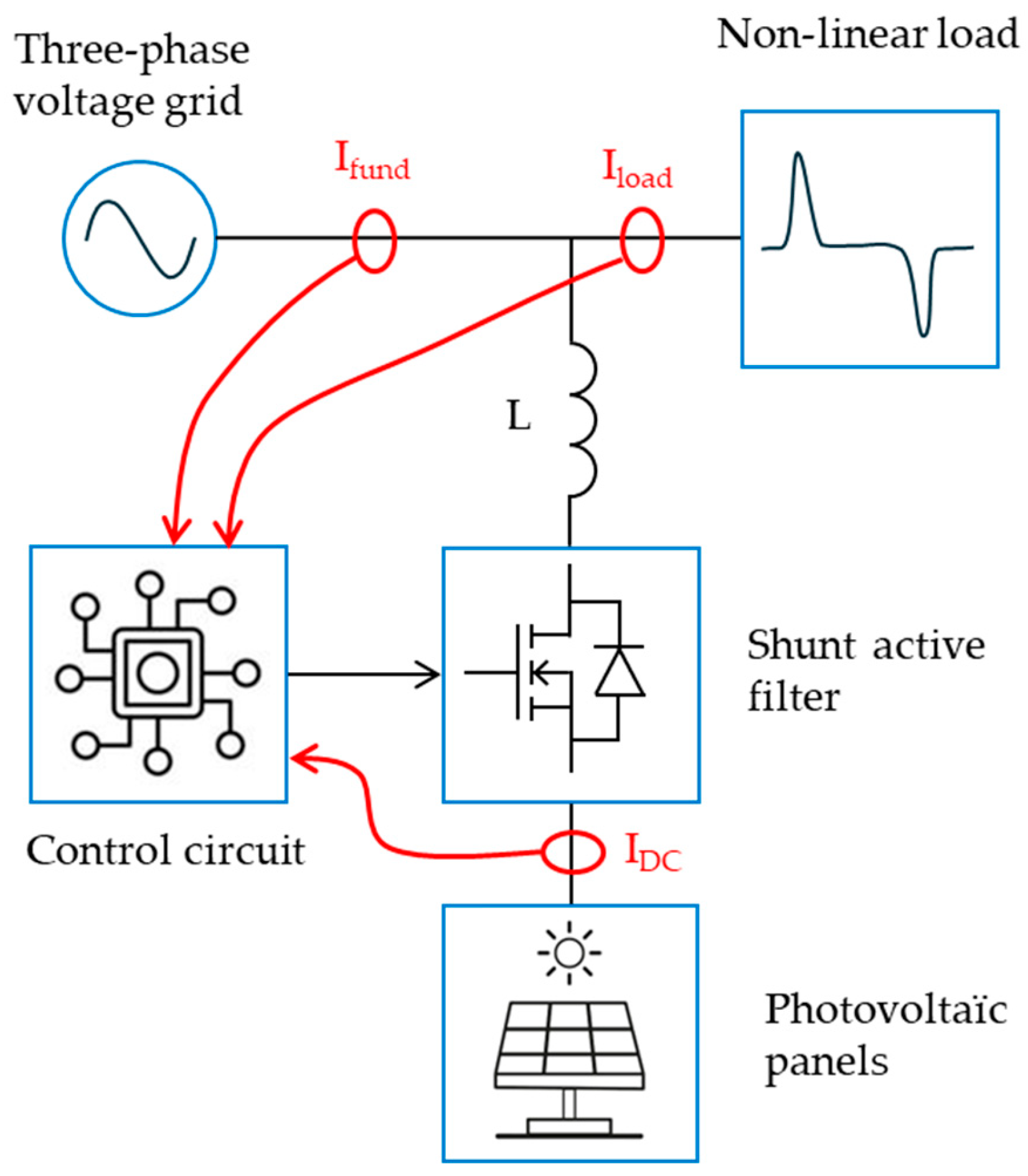
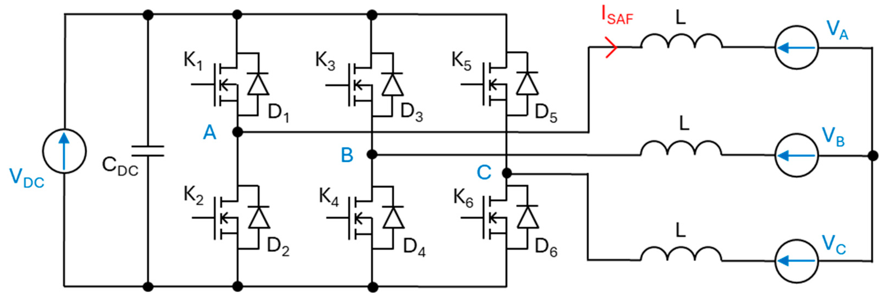
2. Electrical Structure Specifications

The electrical specifications applied to the SAF structure are given in Table 1. The current and voltage RMS values are fixed in addition to the two values of comparison for the switching frequency.
The non-linear load consumes 61 A per phase. Without power injection from the SAF, the grid provides 61 A. With power injection from the SAF, extra power up to 72 A can be added, which feeds the non-linear load. As a consequence, the grid receives an extra 11 A from the SAF. These are the maximal operating values. The value of 800 Vdc was chosen based on the experimental setup already published and referenced as [5] in the manuscript. In [5], the nominal DC voltage was 840 V. This value is normalized to 800 V in the proposed manuscript. Other references use DC voltage values down to 650 V, which is the minimum value to ensure a connection with a 230/400 V 3-phase AC grid. The influence of the DC voltage is investigated in the sixth section of this article.
In accordance with Figure 1, the VSI structure used is a two-level three-phase full bridge with diode D in parallel with transistor K and is given in Figure 2.
Two technologies of transistors are considered in this study: an IGBT for the conventional structure (C-VSI) and a SiC MOSFET (SiC-VSI). For the IGBT, the reference is IKQ50N120CH3, with a voltage rating of 1200 V, a current rating of 65 A at 100 °C, and a unit price of USD 10. For the SiC MOSFET, the reference is C3M0021120K, with an identical voltage rating of 1200 V, a higher current rating of 74 A at 100 °C, and a unit price three times higher of USD 30.

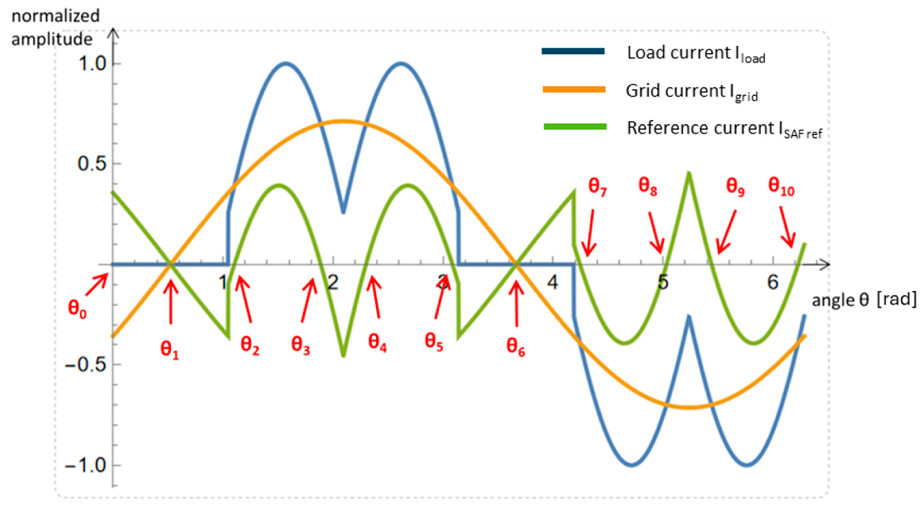
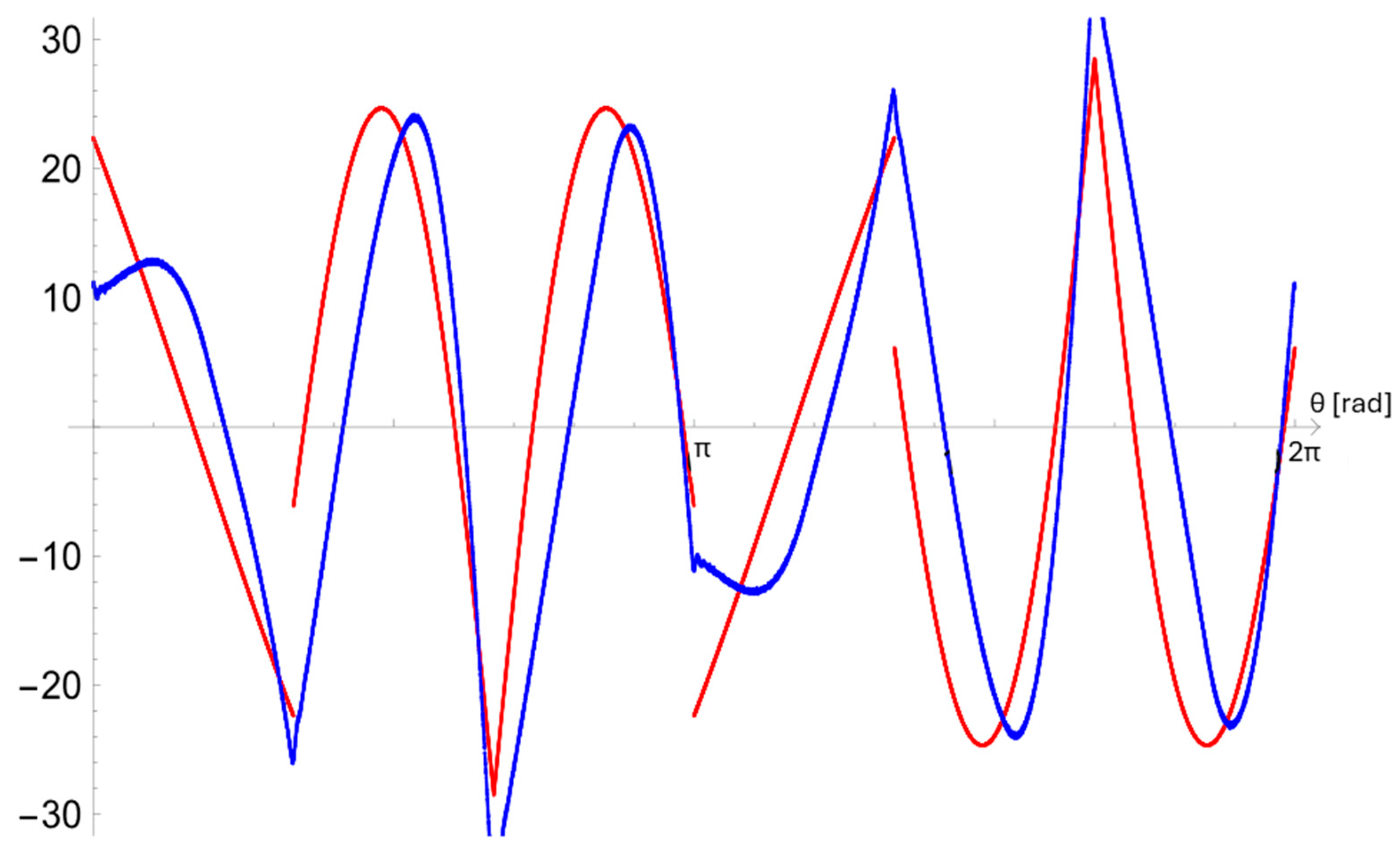
3. Current Waveforms

In a VSI, considering the correct switched current waveform is crucial in order to compute the losses, as it varies all along a low-frequency period in a classic VSI, and as the current variation is all the more singular in the case of harmonic compensation.
In the first case, only the harmonics compensation is considered and therefore the resulting currents waveforms are shown in Figure 3. The modulating signal, which represents the identified harmonics current (ISAFref) in green is then compared with a triangular carrier to generate a PWM signal; see Figure 1. Note that the load current (Iload) corresponds to a non-linear load: a 42 kVA diode full-bridge rectifier with R//C load on the DC side. In addition, the real harmonics current to be produced/injected (ISAFref) by the SAF is obtained by subtracting the fundamental current (Igrid) from the load current (Iload).
The load current is the current absorbed by a three-phase rectifier on a R-C load, with some filtering inductance on the AC side. Each diode conducts during a third of a period, with a double arch current waveform. The exact waveform equation depends on the values of L and C. On one phase leg, the opposite diode conducts during another third of the period. Then, the phase current is the addition of both diode currents. According to the diode polarity, it results in a positive double arch during a third of the period and a negative double arch during another third of the period. During the last third, no diode conducts in the leg, which is why the current is null.
The SAF current (ISAF) is compared, as represented in Figure 4, between the simulation injected current and the model reference. The small difference comes from the delay caused by the inductance/output filter, which prevents the injected current from varying quickly.
In a second case, active compensation with a power injection is considered. The SAF current is then different and is plotted in Figure 5. In this case, a sinusoidal current at the fundamental frequency is added to the harmonic compensation. This current is obtained by the addition of the current from Figure 4 with a sinusoidal current in phase with the grid. The small difference comes from the delay caused by the inductance.

4. SAF Loss Computation

Silicon Carbide (SiC) MOSFET C3M0021120K and IGBT IKQ50N120CH3 are compared, always with the same SiC diode C4D40120H. The methodology to compute losses in power components is depicted in the following lines, first only in the SAF condition (no power injection) and then in the SAF-REG condition (with power injection). Numerical values are computed and compared to a PLECS simulation in Section 5.
The comparison between the PLECS waveform and the mathematical waveform is proposed in Figure 4 and Figure 5. In both cases, the blue curves represent real measurements from a real SAF converter. These curves are saved and used to feed the PLECS simulation. The red curves represent the mathematical model, used for the analytical loss computation. The difference between the PLECS and the mathematical waveforms come from the influence of the SAF inductance, which introduce a small phase-shift and eliminates current discontinuities.

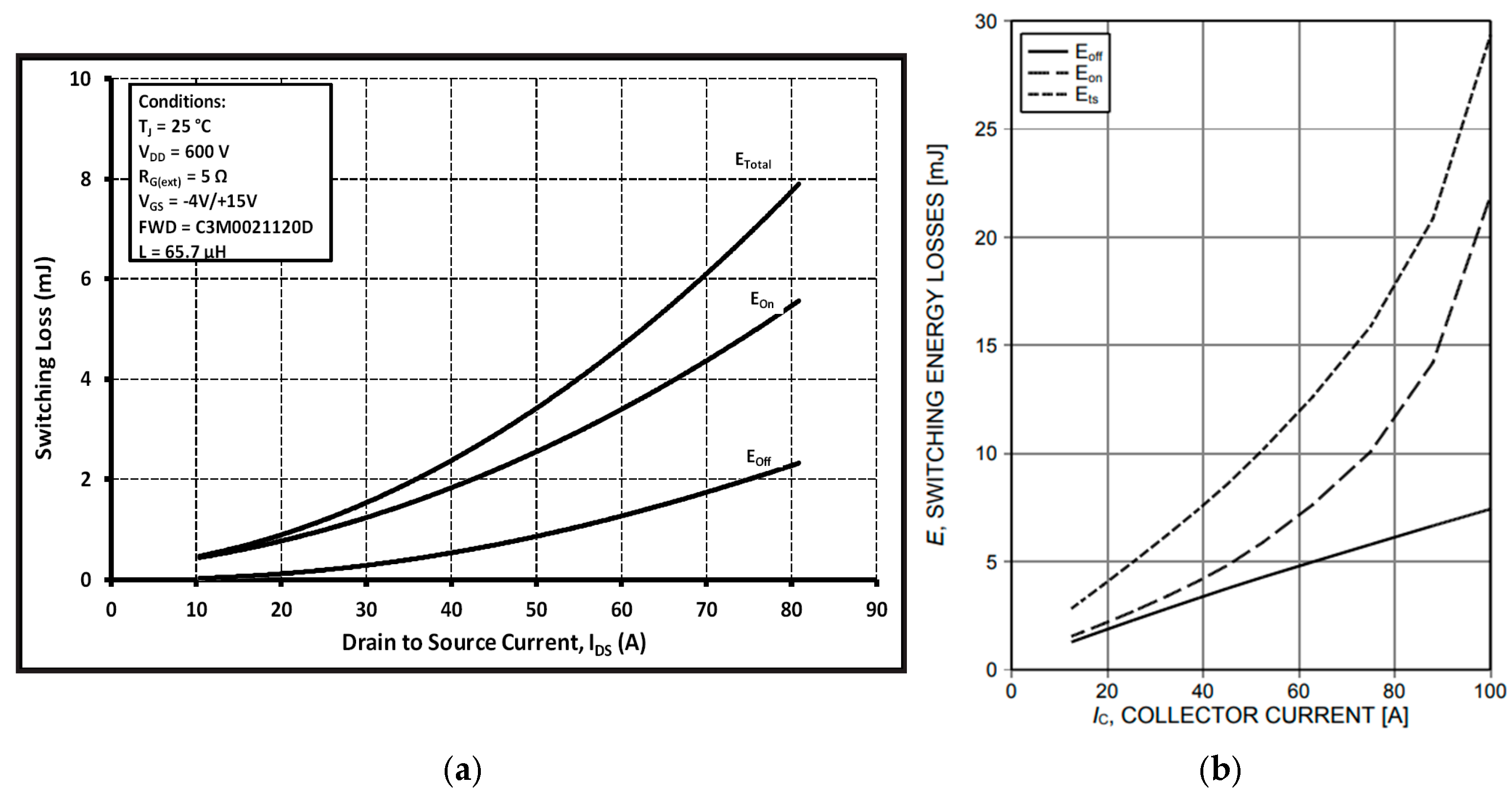
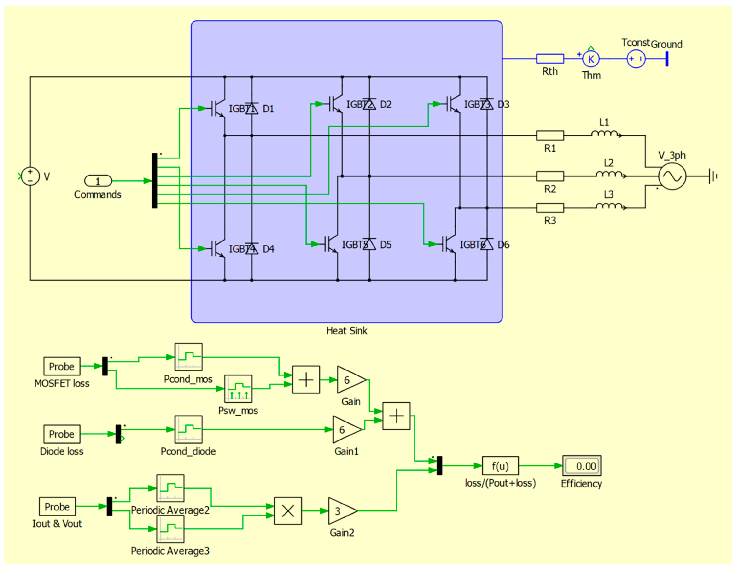
4.1. VSI Loss Computation in the SAF-Only Condition

It is first possible to compute the RMS current injected into a switch as MOSFET K in addition to a diode D with (1).
I K + D   R M S = 1 2 π 0 2 π α θ I S A F ( θ ) 2 d θ
with α(θ) as the duty cycle varying from 0 to 1 in a sinusoidal way, and with ISAF(θ) as the mathematical piecewise SAF current waveform from Figure 5. This current waveform is displayed as applied in PLECS in Figure 6 for a switching frequency of 16 kHz, with power injection.
It is assumed that the positive current flows through the transistor and the negative current through the diode. This assumption is perfectly correct for the IGBT because it is a bipolar component. In the case of the MOSFET, the assumption does not take into account the current that may flow in the reverse direction of the transistor [12].
To obtain the injected current in one transistor K, the integral is separated in five parts, according to the moment when the current is positive. By reason of symmetry, the RMS and average currents in the transistor are expressed in (2) and (3). Angles θi are calculated at the intersection between the fundamental and the polluting load current.
I K R M S = 1 2 π ( 2 θ 0 θ 1 α θ I S A F θ 2 d θ + 2 θ 2 θ 3 α θ I S A F θ 2 d θ + θ 8 θ 9 α θ I S A F θ 2 d θ )
I K   a v e r a g e = 1 2 π ( 2 θ 0 θ 1 α θ I S A F θ d θ + 2 θ 2 θ 3 α θ I S A F θ d θ + θ 8 θ 9 α θ I S A F θ d θ )
Computing the RMS and average current makes it possible to evaluate the conduction losses in a MOSFET and in an IGBT. The general formulation of conduction losses is given in (4). Formulas (5) and (6) are then obtained considering only a resistive impedance RDS on for the MOSFET and a resistance RK0 with a voltage drop VK0 for an IGBT.
P K   c o n d u c t i o n = 1 T v K t . i K t d t
P M O S F E T   c o n d u c t i o n = R D S   o n . I K   r m s 2
P I G B T   c o n d u c t i o n = R K 0 . I K   r m s 2 + V K 0 . I K   a v e r a g e
The switching losses are computed considering the variation in switching energy function of the current, given by the MOSFET or IGBT datasheet. A quadratic interpolation is considered (7) from Figure 7, with Ct as a temperature coefficient chosen at 175 °C.
E t o t I = E o n I + E o f f I = a . I 2 + b . I + c . C t
Then, the switching losses are computed by integration of the switching energy when the current is positive and is multiplied by the switching frequency (8). The method of switching loss computation, developed in (8) and (9), is valid for both MOSFET and IGBT.
P K   s w i t c h i n g = V D C V r e f F d e c 2 π [ 2 θ 0 θ 1 E t o t a l I S A F ( θ ) d θ + 2 θ 1 θ 2 E t o t a l I S A F ( θ ) d θ + θ 8 θ 9 E t o t a l I S A F ( θ ) d θ ]
The current in one diode is computed in a similar way. The integral is separated in five parts, according to the moment when the switched current is negative and then positive in the diode (Equations (9) and (10)).
I D   R M S = 1 2 π ( 2 θ 1 θ 2 α θ I S A F θ 2 d θ + θ 3 θ 4 α θ I S A F θ 2 d θ + 2 θ 7 θ 8 α θ I S A F θ 2 d θ )
I D   a v e r a g e = 1 2 π ( 2 θ 1 θ 2 α θ I S A F θ d θ + θ 3 θ 4 α θ I S A F θ d θ + 2 θ 7 θ 8 α θ I S A F θ d θ )
As the impedance of the diode in the ON state is similar to the IGBT impedance, i.e., resistance and a voltage drop, diode conduction losses are expressed in the same way (11). Recovery losses in the diode are neglected, which is a common assumption when working with SiC Schottky diodes. Finally, the total losses of the converter are expressed in (12).
P D = V D 0 . I D   a v e r a g e + R D 0 . I D   R M S 2
P t o t a l = 6 . ( P K   c o n d + P K   s w i t c h i n g + P D )

4.2. VSI Loss Computation in the SAF-REG Condition

The same methodology is applied in the case of power injection from the photovoltaic system or the batteries. The only difference compared to the previous case lies in the bounds of the integrals for calculating currents and switching losses. Equations (13)–(16) summarize the different expressions.
I K   R M S   P V G = 1 2 π θ 1 θ 6 α θ I S A F θ 2 d θ
I D   R M S   P V G = 1 2 π θ 0 θ 1 α θ I S A F θ 2 d θ + θ 6 θ 10 α θ I S A F θ 2 d θ
I D   a v e r a g e = 1 2 π θ 0 θ 1 α θ I S A F θ d θ + θ 6 θ 10 α θ I S A F θ d θ
P K   s w i t c h i n g = V D C V r e f F d e c 2 π θ 1 θ 6 E t o t a l I S A F ( θ ) d θ

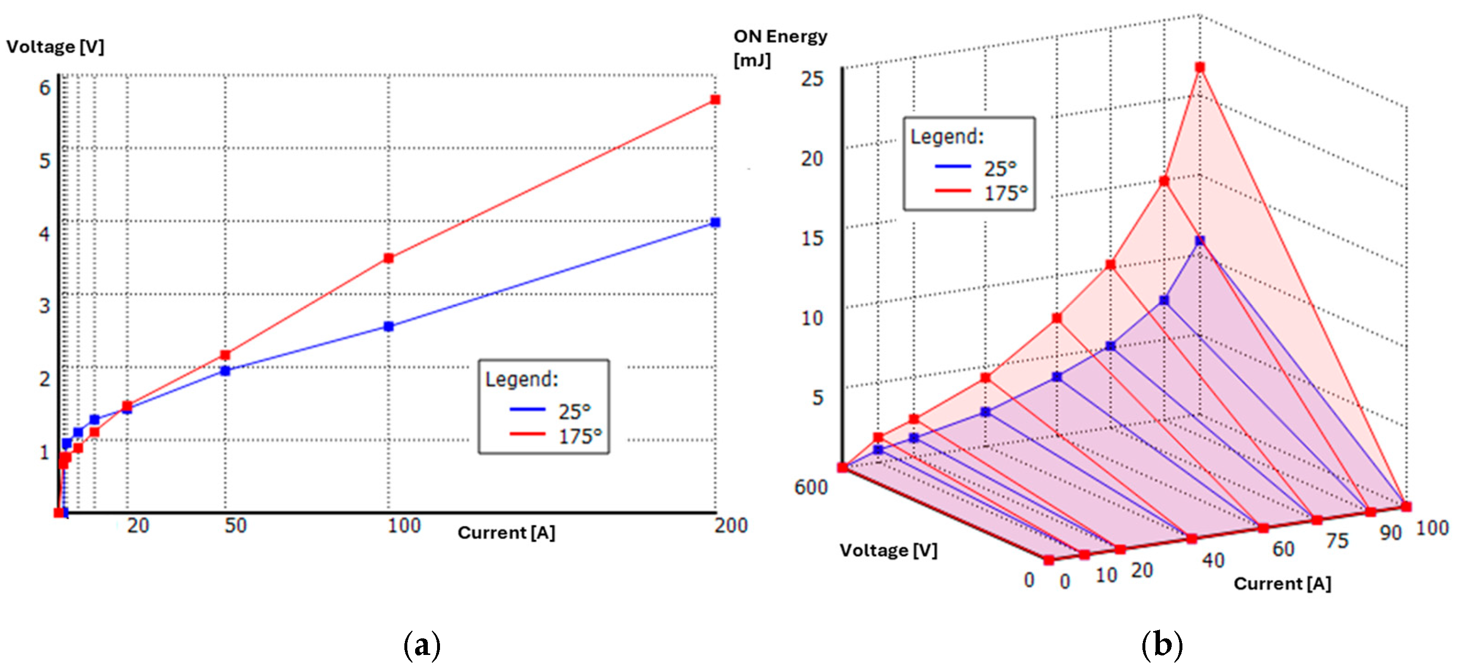
4.3. Design Considerations

The waveform presented in Figure 4, in the case of no power injection, with five cycles per period, is unusual. Then, the classic design approaches to choose the best semiconductor devices is not relevant. In fact, the five cycles lead to a repeated junction temperature variation in the devices, which may damage the components.
In the other case, with power injection, a 50 Hz component is injected in addition to the harmonic compensation. The five cycles are still present, but their effect is mitigated by the 50 Hz component, as can be seen in Figure 5. Therefore, the impact of the harmonic on the junction temperature variation becomes negligible.
In conclusion, a designer should take into account the worst case in the design process when choosing the right devices. In this work, the worst case is presented in Figure 5, when the SAF converter provides harmonic compensation as well as a 50 Hz current. The devices are chosen to handle a more than 100 A peak. In the case of no power injection (Figure 4), the transistors are then oversized, and no overheating or excessive thermal cycling is of concern.

5. Efficiency Comparison Between IGBT and SiC MOSFET

The numerical values are computed and compared to a PLECS simulation in Section 5.
The PLECS schematic used for the simulation is available in Figure 8. The blue rectangle represents the thermal heatsink of the system. It has been verified that the temperature remains between 25 °C and 100 °C according to the different thermal resistances taken into account in the simulation. IGBTs and diodes are modelled in PLECS with data from their manufacturer. Some data examples are provided in Figure 9 for IGBT IKQ50N120CH3. Static and switching energies are given for different temperatures, voltages, and currents. Static characteristics are used to compute conduction losses, while switching energies give the switching losses. The junction temperature of each device depends on the losses of each device, on the ambient temperature, and on the heatsink characteristics. Probes are added to directly measure the instantaneous conduction and switching losses. An average operator is added to obtain the mean value during a grid period.
This framework takes into account many more phenomena than those modelled, such as the variation in junction temperature of components as a function of losses, which influences the static and dynamic characteristics of switches, the impact of dead times, gate resistance, reverse conduction in MOSFETs, non-linearities in characteristics, or thermal impedance with the external environment.
Consequently, as experimental measurements cannot isolate each contribution (conduction, switching, transistor, and diode), the developed models will only be validated with the PLECS framework, which includes data from real measurements carried out by the manufacturer.
In the case of only harmonics compensation, the analytical and simulation results are given in Table 2. The IGBT and MOSFET solutions are compared for switching frequencies of 16 kHz and 100 kHz. The IGBT solution at 100 kHz is not considered because it is too inefficient. In fact, IGBTs are not meant to handle such high switching frequencies, generating too much switching loss and overheating the transistor. Converter efficiency is not displayed in this case as no power is transferred, only harmonics are injected. Therefore, the notion of efficiency is meaningless.
The error between the developed models and the simulation measurements, considering real components, is almost always under 7%. The only significant difference comes from the evaluation of the average current in the diode because of the difference in current waveforms depicted in Figure 4 and because the non-linear behaviour of the diode is simplified in the model. Then, as the overall computed losses are close to the measured losses, the developed models are validated in this case.
In term of analysis, the losses from the VSI-SiC are unsurprisingly lower than those from the C-VSI [20,21,22] at 16 kHz as well as 100 kHz for two reasons. First, the SiC MOSFET consists of wide band gap transistors that exhibit significantly lower switching energies compared to IGBT transistors. Second, as the switched current is very low compared to the current calibre of the transistors, the forward voltage drop from the IGBT has a strong impact.
In the case of compensation with power injection, the results are given in Table 3.
The efficiency is computed with Equation (17), thanks to the converter losses calculated or measured by PLECS.
e f f i c i e n c y = P O U T   S A F P O U T   S A F + c o n v e r t e r   l o s s e s
The difference in conduction losses between 16 kHz and 100 kHz comes from the difference in junction temperature induced by the switching losses, not taken into account in the model, which increases the value of RDS ON.
The SiC MOSFET solution is unsurprisingly better in terms of efficiency for 16 kHz, and even at 100 kHz, as observed in [20,21,22], which deal with only fundamental current injections without harmonic filtering. The 100 kHz solution makes it possible to drastically decrease the size, cost, and losses of the choke inductance/output filter.

6. Efficiency Comparison for Different DC Voltages

Increasing the DC voltage is a conventional solution in order to increase, among other things, the overall SAF dynamics and consequently harmonic filtering. Thus, different DC voltage scenarios are imagined in this section. As the DC voltage increases, the voltage rating of the transistor is adapted. A conventional rule considers that the voltage rating should be higher than 1.5 times the DC voltage, for reliability reasons. Then, a new MOSFET reference has to be used: the C2M0045170P with a voltage rating of 1700 V; a current rating of 48 A at 100 °C; and a unit price three times higher than previously, USD 90. The different cases are as follows:
  • Vdc = 800 V, with MOSFET SiC 1200 V rating (reference case);
  • Vdc = 1000 V, with MOSFET SiC 1700 V rating;
  • Vdc = 1200 V, with MOSFET SiC 1700 V rating.
The converter efficiency is computed in Table 4 and Table 5 for different DC voltages (800 V, 1000 V, and 1200 V), with and without power injection.
The results reveal that efficiency decreases when the DC voltage increases. The first explanation is that increasing the voltage above 800 V forces the designer to use 1700 V components, which have worse properties in addition to an extra cost. The second explanation is based on the switching loss increase, proportional to the DC voltage.

7. Conclusions

A new method for calculating losses and efficiency is developed in this article in the specific case of SAFs. Two cases are developed: the classic case of harmonic compensation of a non-linear load, and the case where power is injected in addition to harmonics. The method developed is the same in both cases, only the integral limits are modified. The models are applicable for any type of switch, in particular MOSFET and IGBT. The point-by-point comparison with manufacturer data allows the developed models to be validated and the limits and points for improvement to be discussed.
The results obtained allow a designer to quickly compare different ranges of components for the design of their SAF. Very few other analytical studies of the state of the art allows for this comparison yet is crucial as we know that energy efficiency represents a real challenge in the design of SAFs.

Author Contributions

Conceptualization, M.A.E.A.; Methodology, A.V.; Software, A.V. and T.P.; Validation, A.V.; Writing—original draft, A.V. and M.A.E.A.; Writing—review & editing, T.P. and M.A.E.A.; Project administration, M.A.E.A. All authors have read and agreed to the published version of the manuscript.

Funding

This research received no external funding.

Data Availability Statement

Data are contained within the article.

Conflicts of Interest

The authors declare no conflict of interest.

References

  1. Fujita, H.; Akagi, H. The unified power quality conditioner: The integration of series- and shunt-active filters. IEEE Trans. Power Electron. 1998, 13, 315–322. [Google Scholar] [CrossRef]
  2. Schaffner. “ECOsine® Active Harmonics Compensation in Real-Time”. August 2015. Available online: https://www.schaffner.com/fileadmin/user_upload/Media/Downloads/installation-manual-operating-instructions-ecosine-activ-REV6.pdf (accessed on 1 April 2025).
  3. Tareen, W.U.; Mekhilef, S.; Seyedmahmoudian, M.; Horan, B. Active power filter (APF) for mitigation of power quality issues in grid integration of wind and photovoltaic energy conversion system. Renew. Sustain. Energy Rev. 2017, 70, 635–655. [Google Scholar] [CrossRef]
  4. Gomes, C.C.; Cupertino, A.F.; Pereira, H.A. Damping techniques for grid-connected voltage source converters based on LCL filter: An overview. Renew. Sustain. Energy Rev. 2018, 81, 116–135. [Google Scholar] [CrossRef]
  5. Alali, M.A.E.; Shtessel, Y.B.; Barbot, J.-P. Grid-Connected Shunt Active LCL Control via Continuous Sliding Modes. IEEEASME Trans. Mechatron. 2019, 24, 729–740. [Google Scholar] [CrossRef]
  6. Jayasankar, V.N.; Vinatha, U. Advanced Control Approach for Shunt Active Power Filter Interfacing Wind- Solar Hybrid Renewable System to Distribution Grid. EBSCOhost 2018, 14, 88. Available online: https://openurl.ebsco.com/contentitem/gcd:129864541?sid=ebsco:plink:crawler&id=ebsco:gcd:129864541 (accessed on 1 April 2025).
  7. Reznik, A.; Simões, M.G.; Al-Durra, A.; Muyeen, S.M. LCL Filter Design and Performance Analysis for Grid-Interconnected Systems. IEEE Trans. Ind. Appl. 2014, 50, 1225–1232. [Google Scholar] [CrossRef]
  8. Imam, A.A.; Sreerama Kumar, R.; Al-Turki, Y.A. Modeling and Simulation of a PI Controlled Shunt Active Power Filter for Power Quality Enhancement Based on P-Q Theory. Electronics 2020, 9, 637. [Google Scholar] [CrossRef]
  9. Raman, R.; Sadhu, P.K.; Kumar, R.; Rangarajan, S.S.; Subramaniam, U.; Collins, E.R.; Senjyu, T. Feasible Evaluation and Implementation of Shunt Active Filter for Harmonic Mitigation in Induction Heating System. Electronics 2022, 11, 3464. [Google Scholar] [CrossRef]
  10. Hoon, Y.; Mohd Radzi, M.A.; Mohd Zainuri, M.A.A.; Zawawi, M.A.M. Shunt Active Power Filter: A Review on Phase Synchronization Control Techniques. Electronics 2019, 8, 791. [Google Scholar] [CrossRef]
  11. Alali, M.A.E.; Sabiri, Z.; Shtessel, Y.B.; Barbot, J.-P. Study of a common control strategy for grid-connected shunt active photovoltaic filter without DC/DC converter. Sustain. Energy Technol. Assess. 2021, 45, 101149. [Google Scholar] [CrossRef]
  12. Acquaviva, A.; Rodionov, A.; Kersten, A.; Thiringer, T.; Liu, Y. Analytical Conduction Loss Calculation of a MOSFET Three-Phase Inverter Accounting for the Reverse Conduction and the Blanking Time. IEEE Trans. Ind. Electron. 2021, 68, 6682–6691. [Google Scholar] [CrossRef]
  13. Madhusoodhanan, S.; Mainali, K.; Tripathi, A.K.; Kadavelugu, A.; Patel, D.; Bhattacharya, S. Power Loss Analysis of Medium-Voltage Three-Phase Converters Using 15-kV/40-A SiC N-IGBT. IEEE J. Emerg. Sel. Top. Power Electron. 2016, 4, 902–917. [Google Scholar] [CrossRef]
  14. Costa, P.; Pinto, S.; Silva, J.F. A Novel Analytical Formulation of SiC-MOSFET Losses to Size High-Efficiency Three-Phase Inverters. Energies 2023, 16, 818. [Google Scholar] [CrossRef]
  15. Wong, M.-C.; Pang, Y.; Xiang, Z.; Wang, L.; Lam, C.-S. Assessment of Active and Hybrid Power Filters Under Space Vector Modulation. IEEE Trans. Power Electron. 2021, 36, 2947–2963. [Google Scholar] [CrossRef]
  16. Wang, L.; Lam, C.-S.; Wong, M.-C. The Analysis of DC-link Voltage, Compensation Range, Cost, Reliability and Power Loss for Shunt (Hybrid) Active Power Filters. In Proceedings of the 2018 IEEE PES Asia-Pacific Power and Energy Engineering Conference (APPEEC), Sabah, Malaysia, 7–10 October 2018; pp. 640–645. [Google Scholar]
  17. Muñoz, J.; Baier, C.; Espinoza, J.; Rivera, M.; Guzmán, J.; Rohten, J. Switching losses analysis of an asymmetric multilevel Shunt Active Power Filter. In Proceedings of the IECON 2013—39th Annual Conference of the IEEE Industrial Electronics Society, Vienna, Austria, 10–13 November 2013; pp. 8534–8539. [Google Scholar]
  18. Wolfspeed. “C3M0021120K Datasheet”. Available online: https://assets.wolfspeed.com/uploads/2024/01/Wolfspeed_C3M0021120K_data_sheet.pdf (accessed on 1 April 2025).
  19. Infineon. “IKQ50N120CH3-DataSheet”. Available online: https://www.infineon.com/dgdl/Infineon-IKQ50N120CH3-DataSheet-v02_04-EN.pdf?fileId=5546d4625bd71aa0015bd817b0150536 (accessed on 1 April 2025).
  20. Nitzsche, M.; Cheshire, C.; Fischer, M.; Ruthardt, J.; Roth-Stielow, J. Comprehensive Comparison of a SiC MOSFET and Si IGBT Based Inverter. In Proceedings of the PCIM Europe 2019; International Exhibition and Conference for Power Electronics, Intelligent Motion, Renewable Energy and Energy Management, Nuremberg, Germany, 7–9 May 2019; pp. 1–7. Available online: https://ieeexplore.ieee.org/abstract/document/8767737 (accessed on 1 April 2025).
  21. Loncarski, J.; Giuseppe Monopoli, V.; Leuzzi, R.; Zanchetta, P.; Cupertino, F. Efficiency, Cost and Volume Comparison of Si-IGBT Based T-NPC and 2-Level SiC-MOSFET Based Topology with dv/dt Filter for High Speed Drives. In Proceedings of the 2020 IEEE Energy Conversion Congress and Exposition (ECCE), Detroit, MI, USA, 11–15 October 2020; pp. 3718–3724. [Google Scholar]
  22. Sivkov, O.; Novak, M.; Novak, J. Comparison between Si IGBT and SiC MOSFET Inverters for AC Motor Drive. In Proceedings of the 2018 18th International Conference on Mechatronics—Mechatronika (ME), Brno, Czech Republic, 5–7 December 2018; pp. 1–5. Available online: https://ieeexplore.ieee.org/abstract/document/8624759 (accessed on 1 April 2025).
Figure 1. Shunt Active Filter with photovoltaic energy generation.
Electronics 14 01972 g001
Figure 2. SAF electrical circuit: three-phase VSI structure.
Electronics 14 01972 g002
Figure 3. Current waveforms over one period.
Electronics 14 01972 g003
Figure 4. SAF current waveform: simulation in blue; model in red.
Electronics 14 01972 g004
Figure 5. SAF current waveform with power injection: simulation in blue; model in red.
Electronics 14 01972 g005
Figure 6. Current waveforms with power injection: in a MOSFET K (middle), in a diode D (bottom), and in both (top).
Electronics 14 01972 g006
Figure 7. Evolution of the switching energy function of the current from (a) the MOSFET C3M0021120K datasheet [18] and (b) the IGBT IKQ50N120CH3 datasheet [19].
Electronics 14 01972 g007
Figure 8. PLECS schematic used to measure the losses of the SAF.
Electronics 14 01972 g008
Figure 9. (a) Static characteristics and (b) ON switching energy of IGBT IKQ50N120CH3 defined in PLECS by the manufacturer.
Electronics 14 01972 g009
Table 1. Main input data of the studied SAF.
SymbolParameterUnitValue
VdcDC voltageV800
VsRMS phase-to-neutral PCC voltageV230
VfundFundamental/grid frequencyHz50
VswSwitching frequencykHz16 and 100
IloadRMS current in the non-linear loadA61
ISAFRMS current in the SAFA72
IgridRMS current from or to the gridA+61 without power injection
−11 with power injection
Table 2. Power losses comparison of SiC-MOSFET and IGBT for the harmonic filtering case.
ParameterModelSimulationError [%]
SAF current15.8 A15.9 A0.3
RMS current in transistor + diode11.1 A11.1 A0.1
RMS current in transistor8.38 A8.27 A1.3
Average current in transistor3.59 A3.81 A5.8
RMS current in diode7.32 A7.48 A2.1
Average current in diode2.35 A3.00 A22
Diode conduction losses3.22 W3.61 W11
Diode recovery lossesneglectedneglected-
MOSFET solution at 100 kHz
MOSFET conduction losses2.11 W2.22 W5.0
MOSFET switching losses21.0 W19.8 W6.0
MOSFET total losses23.1 W22.0 W5.0
Converter losses158 W154 W2.5
MOSFET solution at 16 kHz
MOSFET conduction losses1.53 W1.60 W5.0
MOSFET switching losses3.43 W3.59 W4.5
MOSFET total losses4.96 W5.19 W4.4
Converter losses48.2 W51.8 W6.9
IGBT solution at 16 kHz
IGBT conduction losses5.10 W4.51 W13
IGBT switching losses26.3 W25.2 W4.3
IGBT total losses31.4 W29.7 W5.7
Converter losses207 W200 W3.5
Table 3. Power loss comparison of SiC-MOSFET and IGBT for the power generation case.
ParameterModelSimulationError [%]
SAF current72.2 A72.1 A0.1
RMS current in transistor + diode50.3 A51.2 A1.8
RMS current in transistor46.0 A46.2 A0.4
Average current in transistor25.8 A26.1 A1.1
RMS current in diode20.5 A22.2 A7.7
Average current in diode6.05 A7.20 A16
Diode conduction losses13.6 W13.8 W14
Diode recovery lossesneglectedNeglected-
MOSFET solution at 100 kHz
MOSFET conduction losses75.6 W77.7 W2.7
MOSFET switching losses135 W133 W1.5
MOSFET total losses211 W211 W0.1
Converter losses1339 W1347 W0.6
Efficiency97.1%97.1%-
MOSFET solution at 16 kHz
MOSFET conduction losses63.5 W62.7 W1.3
MOSFET switching losses21.6 W18.0 W20
MOSFET total losses85.1 W80.7 W5.4
Converter losses587 W570 W3.0
Efficiency98.7%98.8%-
IGBT solution at 16 kHz
IGBT conduction losses78.776.23.3
IGBT switching losses1651660.6
IGBT total losses2442420.8
Converter losses153915370.1
Efficiency96.6%96.6%-
Table 4. SiC-MOSFET power loss calculations under different DC voltages for the harmonic filtering case.
ParameterModelSimulationError [%]
800 Vdc solution
MOSFET conduction losses2.11 W2.22 W5.0
MOSFET switching losses21.0 W19.8 W6.0
MOSFET total losses23.1 W22.0 W5.0
converter losses158 W154 W2.5
1000 Vdc solution
MOSFET conduction losses2.91 W2.62 W11
MOSFET switching losses27.2 W28.7 W5.2
MOSFET total losses30.1 W31.3 W3.8
Converter losses204 W211 W3.1
1200 Vdc solution
MOSFET conduction losses2.85 W2.54 W13
MOSFET switching losses32.9 W34.1 W3.5
MOSFET total losses35.8 W36.6 W2.2
Converter losses239 W243 W1.7
Table 5. SiC-MOSFET power loss calculations under different DC voltages for the generation case.
ParameterModelSimulationError [%]
800 Vdc solution
MOSFET conduction losses75.6 W77.7 W2.7
MOSFET switching losses135 W133 W1.5
MOSFET total losses211 W211 W0.1
Converter losses1339 W1347 W0.6
Efficiency97.1%97.1%-
1000 Vdc solution
MOSFET conduction losses146 W142 W2.8
MOSFET switching losses116 W120 W3.3
MOSFET total losses262 W262 W0.0
Converter losses1.66 kW1.66 kW0.0
Efficiency96.3%96.3%-
1200 Vdc solution
MOSFET conduction losses138 W137 W0.7
MOSFET switching losses139 W146 W4.8
MOSFET total losses277 W283 W2.1
Converter losses1.75 kW1.79 kW2.2
Efficiency96.2%96.1%-
Disclaimer/Publisher’s Note: The statements, opinions and data contained in all publications are solely those of the individual author(s) and contributor(s) and not of MDPI and/or the editor(s). MDPI and/or the editor(s) disclaim responsibility for any injury to people or property resulting from any ideas, methods, instructions or products referred to in the content.

