Article

An Upgrade of Radio Frequency Reference Generation and Distribution Modules for FLASH2020+

1
Institute of Electronic Systems, Warsaw University of Technology, 00-665 Warsaw, Poland
2
Deutsches Elektronen-Synchrotron DESY, 22607 Hamburg, Germany
*
Author to whom correspondence should be addressed.
Electronics 2025, 14(1), 173; https://doi.org/10.3390/electronics14010173
Submission received: 14 November 2024 / Revised: 27 December 2024 / Accepted: 30 December 2024 / Published: 3 January 2025
(This article belongs to the Section Microwave and Wireless Communications)

Abstract

:
Free-Electron Laser in Hamburg (FLASH), first launched in 2005, was the first free-electron laser that provided ultrashort radiation pulses in extreme ultraviolet and soft X-ray spectral range. In 2017, it was decided to improve the existing FLASH facility within the FLASH2020+ project, which led to upgrading the existing linac with variable gap tunable undulators in the FLASH1 line and refurbishing two cryomodules to achieve a beam energy increase to 1.35 GeV. It was also a perfect opportunity to completely redesign and rebuild the radio frequency (RF) phase reference generation and distribution system. This paper presents the design and parameters of new, custom-made phase reference signal generation and distribution modules, successfully installed in FLASH. These are the main oscillator, the RF distribution module, and the frequency conversion modules. The new instrumentation presents a significant improvement in terms of RF reference signal parameters, state-of-the-art phase noise performance (an improvement in the total jitter of the 1.3 GHz RF signal from 55.9 fs to 10.7 fs in the integration range from 10 Hz to 1 MHz), module compactness (size reduction from three fully occupied rack cabinets to four 19″ modules only), and serviceability. The presented Main Oscillator system design is foreseen for easy modifications, making it suitable for applications in other accelerator facilities or hardware platforms.

Graphical Abstract

1. Introduction

The scientific case for the upgrade program of the FLASH facility took shape during a user workshop in 2017, where crucial end-user requests and plans were defined [1]. A requirement for a refurbishment and an upgrade of the accelerator arose, as some of its components had been in operation for 15 years. The FLASH2020+ project included replacing the fixed gap undulators in the FLASH1 line with variable gap ones, which led to the possibility of wavelength tuning and a significant reduction in accelerator tuning time and, thus, an increase in available user time. Next, the upgrade program included the application of external seeding to achieve fully coherent pulses of Free-Electron Laser (FEL) light and gain the ability to control the temporal shape and phase of the pulses at the same time in the extreme ultraviolet and soft X-ray spectral range [2]. An upgrade has been performed to achieve a maximum beam energy increase from 1.25 GeV to 1.35 GeV. The shutdown was a perfect time to remove the old Main Oscillator (MO) modules and replace them with new, more compact ones that are used in linac control, instrumentation, and timing. The new modules are compatible with the European XFEL (E-XFEL) MO structure and diagnostic system, and are far easier for maintenance and service repairs. They provide better phase noise performance than previous designs created for FLASH and E-XFEL. To the best of the authors’ knowledge, only a few papers cover the MO design at the same or comparable operating frequencies and with comparable phase noise performance. In [3], the MO is based on a 10 MHz crystal oscillator and a 1.3 GHz phase-locked loop (PLL). The other frequencies are synthesized in a series of frequency dividers. Compared to the solution presented in the paper, the 1.3 GHz performance is worse in the whole frequency test range and there is no information on other frequencies. In [4,5], MO uses the GPS signal as a 10 MHz reference signal. A 704 MHz signal is synthesized with a PLL and other frequencies with a distribution unit. The solution in [6] is based on a 119 MHz signal source and RF frequency multipliers units for the 2856 MHz and 404.6 MHz signals. The last two references do not include phase noise measurement results. The main oscillator in the SINBAD-ARES facility [7,8] offers similar performance to the presented system. It is made of several 19″ modules, separate for the 1000 MHz synthesis, 3000 MHz DRO, and the high power amplifier. The closest match to the presented solution, both in terms of application and achieved results, is published in [9,10]. The mentioned system synthesizes and distributes the 476 MHz reference signal over 1.5 km length to 16 receivers. Receivers are fitted with ultra-low noise Dielectric Resonator Oscillators (DROs) that are used to upconvert the signals to 2856 MHz, while maintaining low phase noise of the reference signal. The total price of the system, due to multiple DROs, is high, and the final performance in terms of phase noise is slightly worse when frequency-scaled and compared to the upgraded FLASH system (approx. 14 fs total jitter in the integration range from 10 Hz to 10 MHz, compared to 10.84 fs in FLASH in the same integration range). Other designed and installed phase reference distribution systems and components [11,12,13,14,15] should also be referenced.
It should also be declared that this paper reuses some content from the PhD thesis [16] with permission.

2. The Former FLASH RF Reference Generation and Distribution System

The old FLASH RF reference generation and distribution modules occupied three rack cabinets in total, and delivered the following reference signal frequencies: 1 MHz, 9 MHz, 13.5 MHz, 27 MHz, 81 MHz, 108 MHz, 1.3 GHz, 1.517 GHz, and 2.856 GHz, all based on a 9 MHz oven-controlled crystal oscillator (OCXO) signal. After over 15 years of reliable operation, modifications, and upgrades, some of the generated frequencies were not needed anymore. Some internal quartz crystal generators showed aging effects as they approached their end-of-life time. This lead to reduced reliability, limited performance, and a potential failure of the entire accelerator machine. Therefore, a completely redesigned system was required for the RF reference signal generation and distribution.

3. Specification and Requirements for Upgraded RF Generation and Distribution System

The most important parameters are listed in Table 1 [17].
As described in [17], the requirements for an upgraded system for FLASH were both hard (strictly defined by end users or obtained by reverse engineering of the existing system) and soft (defined, to be considered more as expected values of some parameters, not always available as a direct value or explicitly specified). These are marked in Table 1 as hard-defined (H) and soft-defined (S) parameters. Having the requirements stated in such a way, the general goal was to deliver a system providing the best performance within available resources and technology at the moment of its creation, and possibly better than the system for the E-XFEL, especially in terms of the phase noise of the 1.3 GHz RF reference signal. Among other requirements for the new system, the backward compatibility with the existing E-XFEL MO and its diagnostic system (accessible via the DOOCS control system [18]), and a simplification of mechanical complexity are the most important.

4. Upgraded RF Generation and Distribution System for FLASH2020+

The block diagram of the upgraded RF generation and distribution system is presented in Figure 1 [16,19].
The structure is based on the E-XFEL Main Oscillator, developed by Warsaw University of Technology and DESY. The main reference is a highly stable 10 MHz signal, provided by a commercial 19″ GPS Disciplined Oscillator (GPSDO) module GPS10eR by Precision Test Systems. That signal is then routed to the input of the new FLASH MO (FL-MO1300) module, which upconverts it to a 1.3 GHz high power signal for a Flash Distribution Module (FL-DISM) and a lower power signal for the Frequency Conversion Module (FL-FCM). The FCM for the RF gun (FCM GUN) is a separate device, delivering an extra 27.08(3) MHz and 13.541(6) MHz signals. All of the 19″ modules rely on a similar design based on provided by DESY Temperature Monitor and Control Board (TMCB) [20] for diagnostics and control, the Fuse and Relay Board (FRED) [20] for DC power control and an E-XFEL-like power supply. This architecture is typical for LLRF systems deployed at FLASH and E-XFEL. It is particularly important, as sharing the same diagnostic scheme and components between managed accelerator systems improves the robustness and operability, and reduces the maintenance time. All of the modules are, therefore, designed to be compatible with the existing DESY E-XFEL system in terms of mechanics, outer design, labeling, and diagnostic and control systems.

5. FLASH Main Oscillator 19″ Module

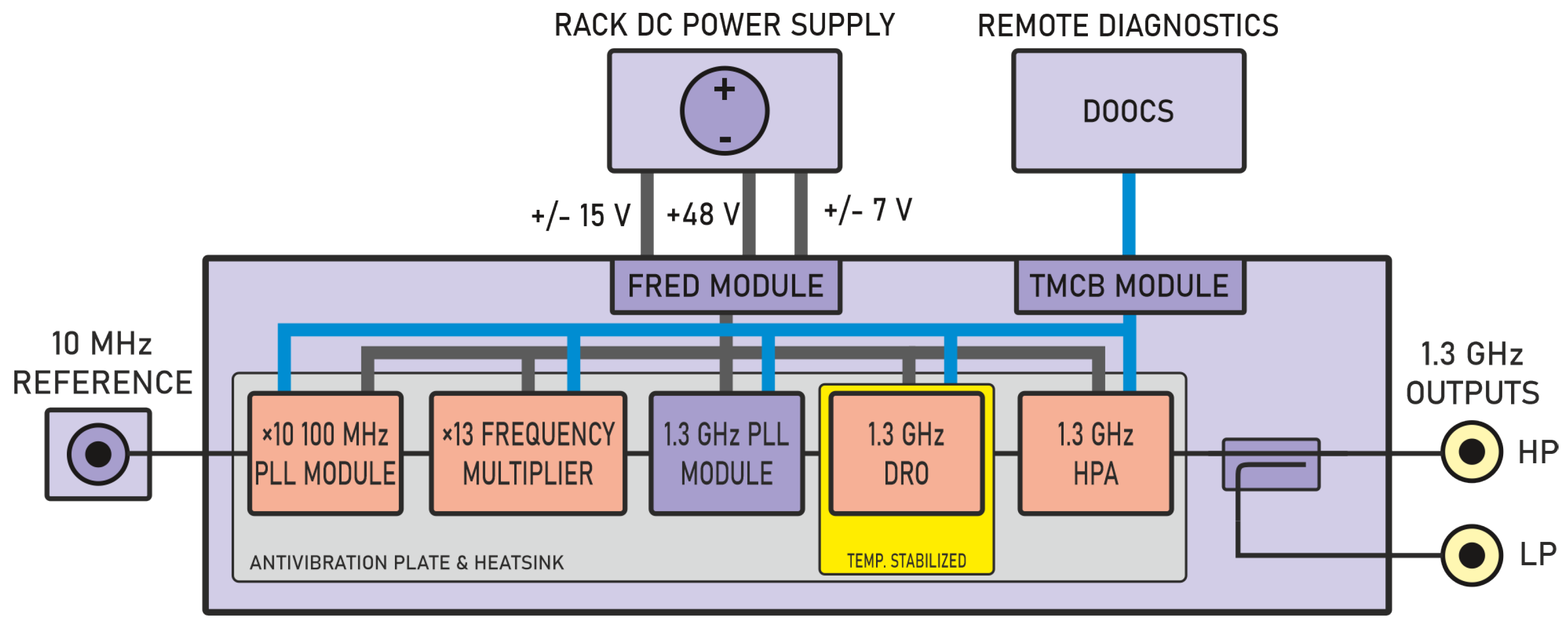
The 19″ FLASH Main Oscillator Module block diagram is shown in Figure 2. The module is compliant with the E-XFEL MO structure. The 100 MHz PLL, 1.3 GHz High-Power Amplifier (HPA), 1.3 GHz Dielectric Resonator Oscillator (DRO), and ×13 Frequency Multiplier are commercially available devices. The 1.3 GHz PLL module has been developed by the Warsaw University of Technology (WUT), and the power supply, remote diagnostics, FRED, and TMCB were provided by DESY.
The principle of operation is based on synchronizing the ultra-low noise DRO output signal with the 1.3 GHz signal synthesized from an ultra-stable GPSDO 10 MHz signal. A key difference between the new and old designs is at the conceptual level. In the old MO, almost all signals were created in a single synthesizer module. In the new design, the MO synthesizes only the 1.3 GHz signal; all other signals are synthesized by the FCM module. Such an approach allowed for the integration of a high-power amplifier in the MO module.
A typical solution to synthesize a 1.3 GHz signal is by using a PLL circuit with a frequency divider in a feedback loop. Using the general theory of signal modulation, a simple model of total Phase Noise (PN) Power Spectral Density (PSD, S ϕ t o t ) can be obtained [16]. The model assumes that the phase noise contributions are not correlated, and the system may be considered as Linear Time Invariant (LTI). Therefore, the contributions are described as a sum, as in Formula (1) [16].
S ϕ t o t ( f ) = S r e f o u t ( f ) + S P H D o u t ( f ) + S F D I V o u t ( f ) + S D R O o u t ( f ) = = S r e f ( f ) + S P H D ( f ) + S F D I V ( f ) · 1 H ( f ) 2 G ( f ) H ( f ) 1 + G ( f ) H ( f ) 2 + S D R O ( f ) · 1 1 + G ( f ) H ( f ) 2
In Formula (1) S ϕ t o t ( f ) is the total phase noise PSD at the output of the MO PLL-based synthesizer; S r e f o u t ( f ) , S P H D o u t ( f ) , S F D I V o u t ( f ) , and S D R O o u t ( f ) are the contributions of, respectively, the reference source, the phase detector, the frequency divider, and the DRO to the total MO phase noise PSD at its output. The G ( f ) , H ( f ) = 1 N are transfer functions of the PLL forward path and the divider in the PLL feedback loop, respectively. S r e f ( f ) , S P H D ( f ) , S F D I V ( f ) , and S D R O ( f ) are the phase noise of the reference source, the phase detector, the frequency divider, and the DRO, measured at their outputs. N is the frequency division ratio of the divider, represented as a positive integer. Output phase noise may be improved by replacing the frequency divider in the feedback loop with a carefully selected frequency multiplier at the input of the PLL. There are two main factors to the improvement. The first one is the removal of the N 2 factor from the noise contribution of the phase detector. Another one is the complete removal of frequency divider contribution, which is usually the main limiting factor for the floor of the in-loop phase noise. While a good frequency multiplier might be comparable with the best frequency dividers in terms of the phase noise floor, the multiplier’s effective noise contribution S M U L T ( f ) is not scaled by the N 2 factor. In the described system, the × 10 PLL frequency multiplier was used to increase the GPSDO signal frequency to 100 MHz, followed by an active frequency multiplier ×13, and finally a phase-locked DRO without a frequency divider in the PLL. The ×10 100 MHz PLL multiplier takes the advantage of a high-performance OCXO to multiply the 10 MHz signal frequency while filtering the far-from carrier GPSDO phase noise. Therefore, for the solution used in the FL-MO1300, Formula (2) is more suitable to represent the total phase noise at the output [16]. As described above, the proposed approach results in a better overall phase noise performance of the MO output signal. It was utilized both in the MO for the E-XFEL, the final MO design for FLASH, and may also be used in other RF reference signal sources of ultra-low phase noise.
S ϕ t o t ( f ) = S r e f o u t ( f ) + S M U L T o u t ( f ) + S P H D o u t ( f ) + S D R O o u t ( f ) = = S r e f ( f ) · N 2 + S P H D ( f ) + S M U L T ( f ) · G ( f ) 1 + G ( f ) 2 + S D R O ( f ) · 1 1 + G ( f ) 2
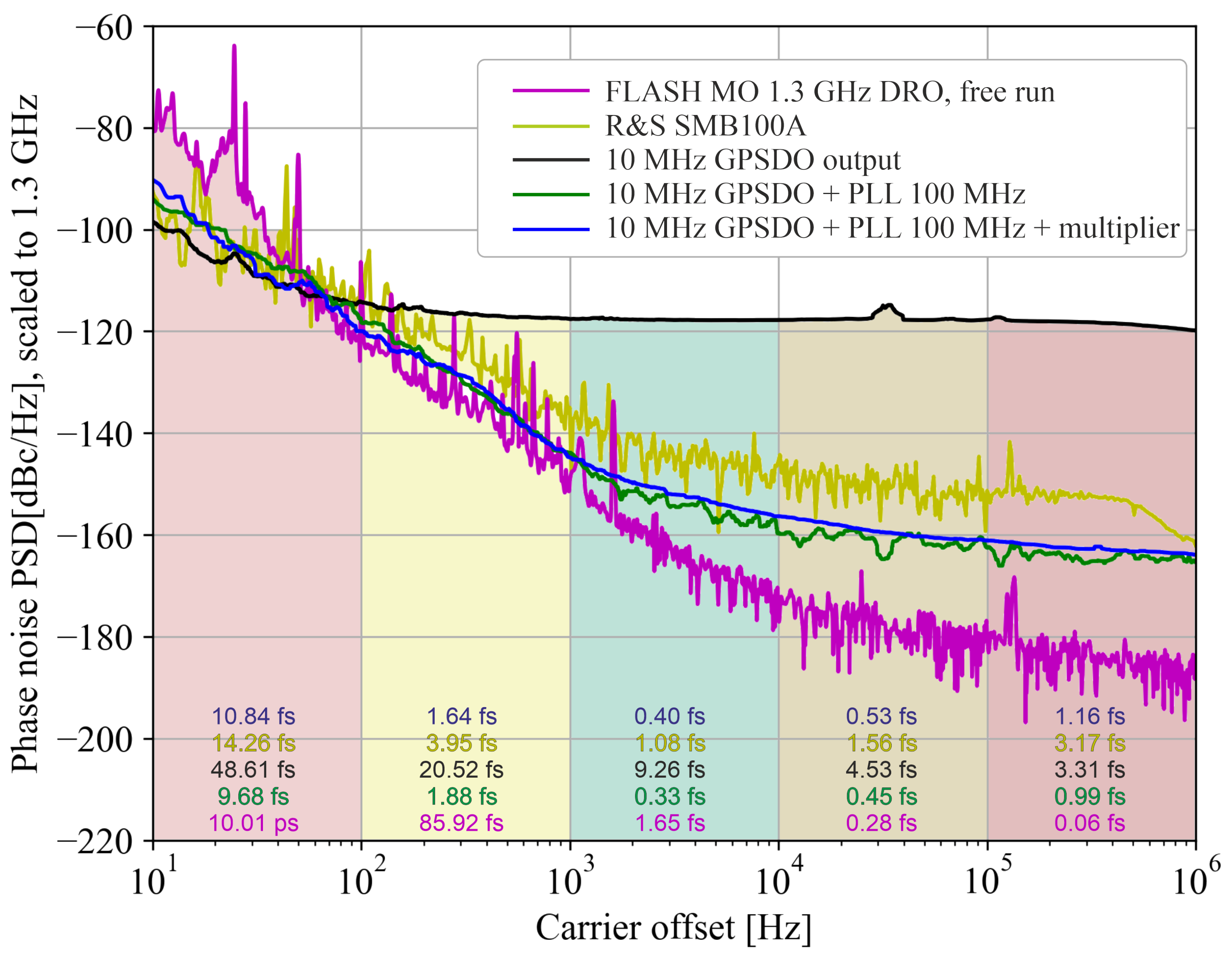
Measured phase noise PSD for selected FL-MO1300 components and cascade configurations are shown in Figure 3 [16]. A high-performance Rohde & Schwarz SMB100A commercial RF synthesizer phase noise is shown for comparison. All of the plots are normalized to 1.3 GHz frequency, and the jitter in selected frequency bands is calculated. The GPSDO provides low phase noise in the close-to-carrier offset frequency range within the PLL bandwidth. Outside the 100 MHz PLL bandwidth (up to 1 Hz), the low phase noise level is determined by the 100 MHz OCXO, giving the optimum phase noise characteristic. Next, the frequency is multiplied by ×13, and the phase noise is slightly increased by the multiplier, which has a small impact on the MO output frequency within the 1.3 GHz PLL bandwidth (in this case above 1 kHz carrier offset frequency). Finally, the 1.3 GHz PLL with the DRO determines the far-from carrier PN PSD levels. The approach improves the total phase noise PSD, especially in the middle-frequency offset range (1 kHz to 100 kHz).
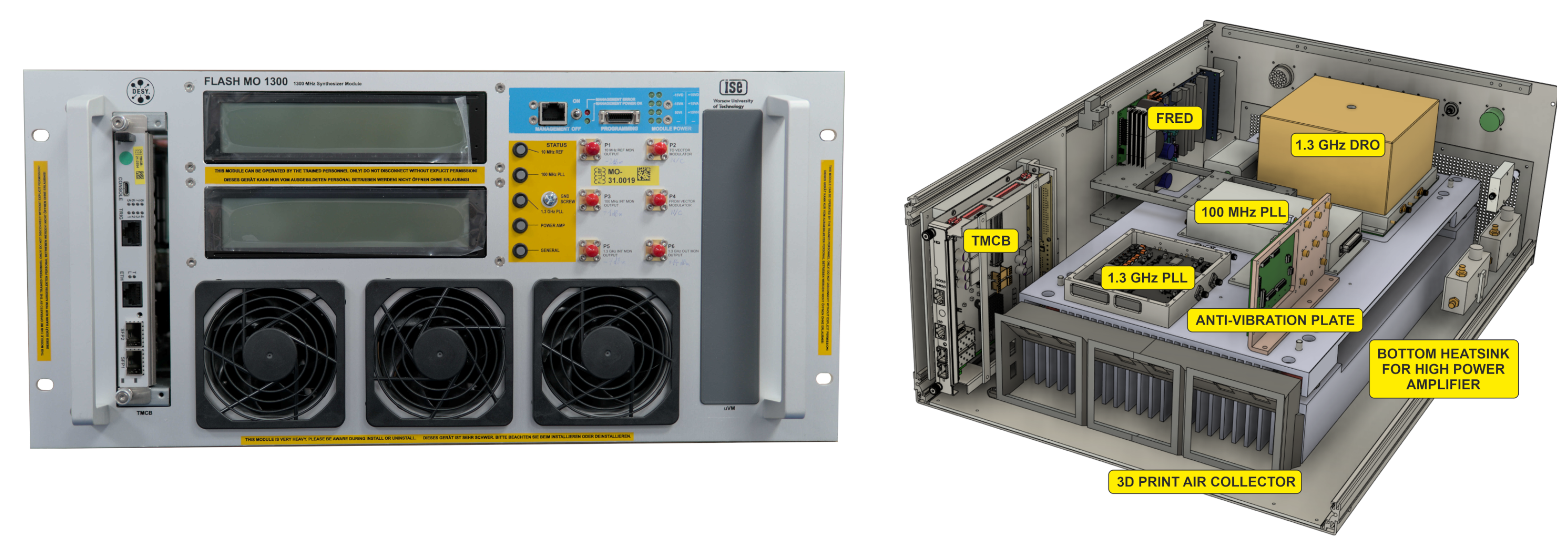
The design view of the FLASH MO module is shown in Figure 4 [16].
All of the inputs and outputs are located in the rear panel, and diagnostic outputs and displays are in the front panel. The described MO mechanical design solves most of the maintenance and service problems of the previous E-XFEL design. The module is made of several layers to efficiently utilize the available space. The lowest layer is made of a large heatsink and a custom 3D-printed air collector for the RF power amplifier. This solution provides good thermal parameters and cooling for the amplifier and controls the airflow within the 19″ module. The heavy heatsink is a perfect base for the upper anti-vibration plate. This plate is mounted on special vibration dampers, and hosts all of the vibration-sensitive parts, like the ×13 multiplier and the DRO [21]. The most fragile component, the DRO, is installed on a thermal insulating plate, and is enclosed by a 3D-printed thermal insulator. Digital control devices are located at the side wall of the module. All the RF and signal cables are routed through a special diagnostic hub to control all potential ground loops within the MO module. For easy access to the internal parts of the module, the front, rear, and side panels may be removed.

6. FLASH Signal Distribution Module

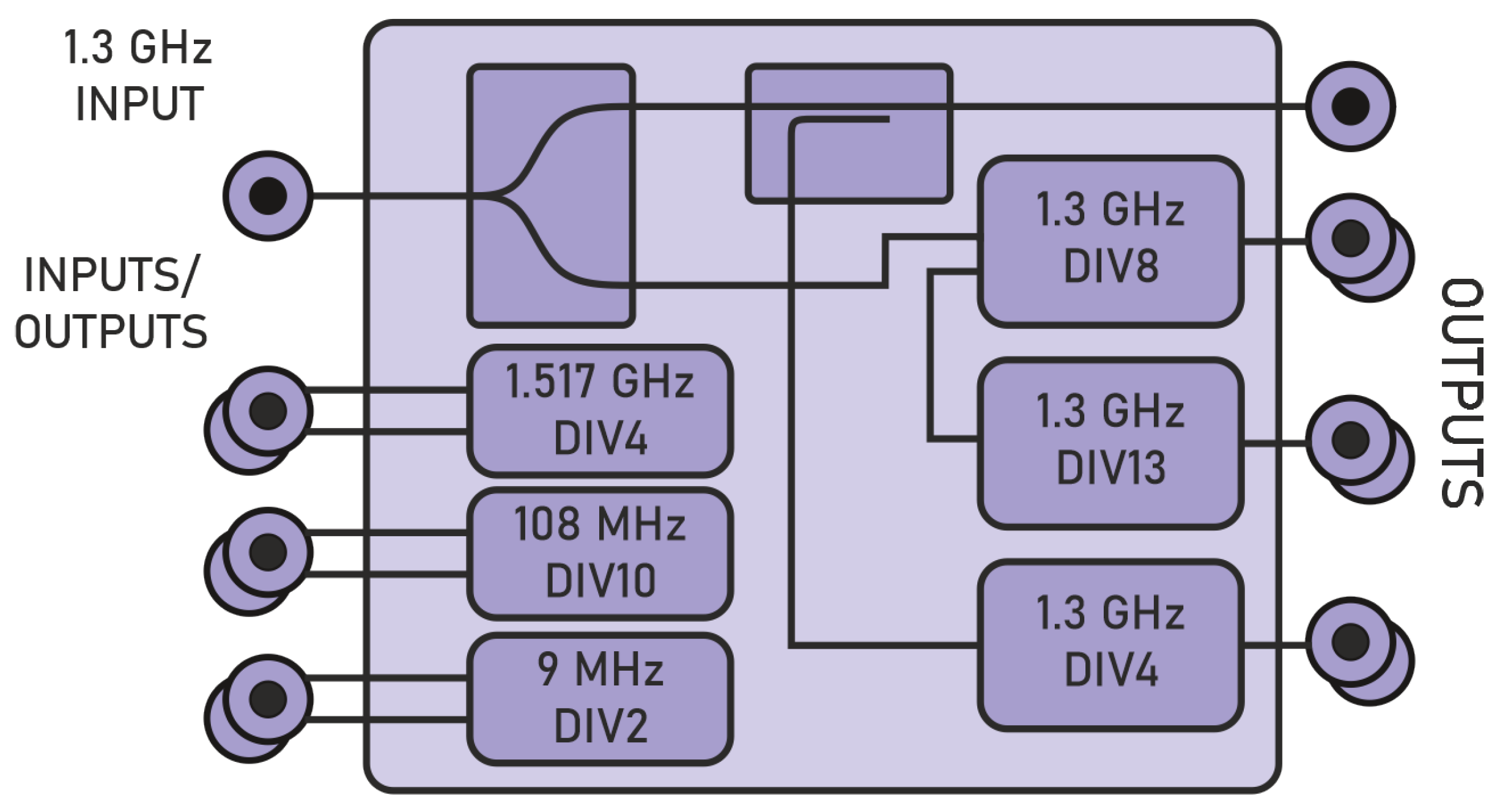
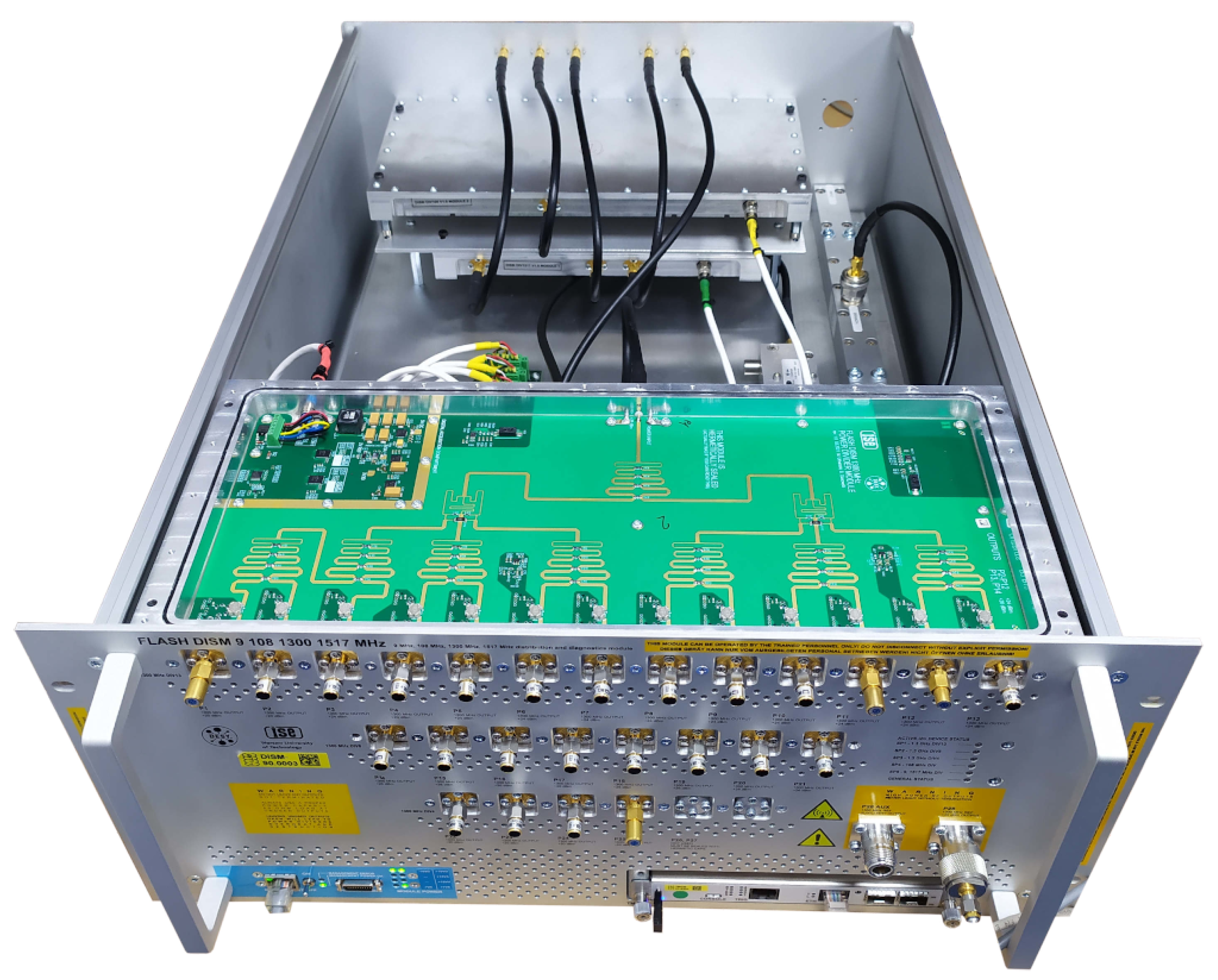
The high power 1.3 GHz signal from the FL-MO1300, and low power signals from FL-FCM, are further split within the FL-DISM to deliver the 9 MHz, the 108 MHz, the 1300 MHz, and the 1517 MHz reference signals to the accelerator subsystems [19]. The internal structure is simple (Figure 5), yet its complexity unfolds in detail and custom-made internal devices, like power splitters. The splitters were designed to assure robust and compact structure with minimum internal cabling to reduce the influence of vibrations on signal phase stability and system reliability, as shown in Figure 6. The splitters are low-loss RF printed circuit boards (PCBs) enclosed in hermetically sealed metal housings, and they are optimized for low insertion loss, input, and output return loss. Output channels are fitted with embedded reflectometer circuits that are used to monitor output power levels and output reflection coefficients. Dividers are all equipped with temperature and humidity sensors. The FL-DISM module provides 26 outputs at 1.3 GHz, four outputs at 1.517 GHz, ten outputs at 108 MHz, and two outputs at 9 MHz (one for diagnostic purposes only).

7. FLASH Frequency Conversion 19″ Module

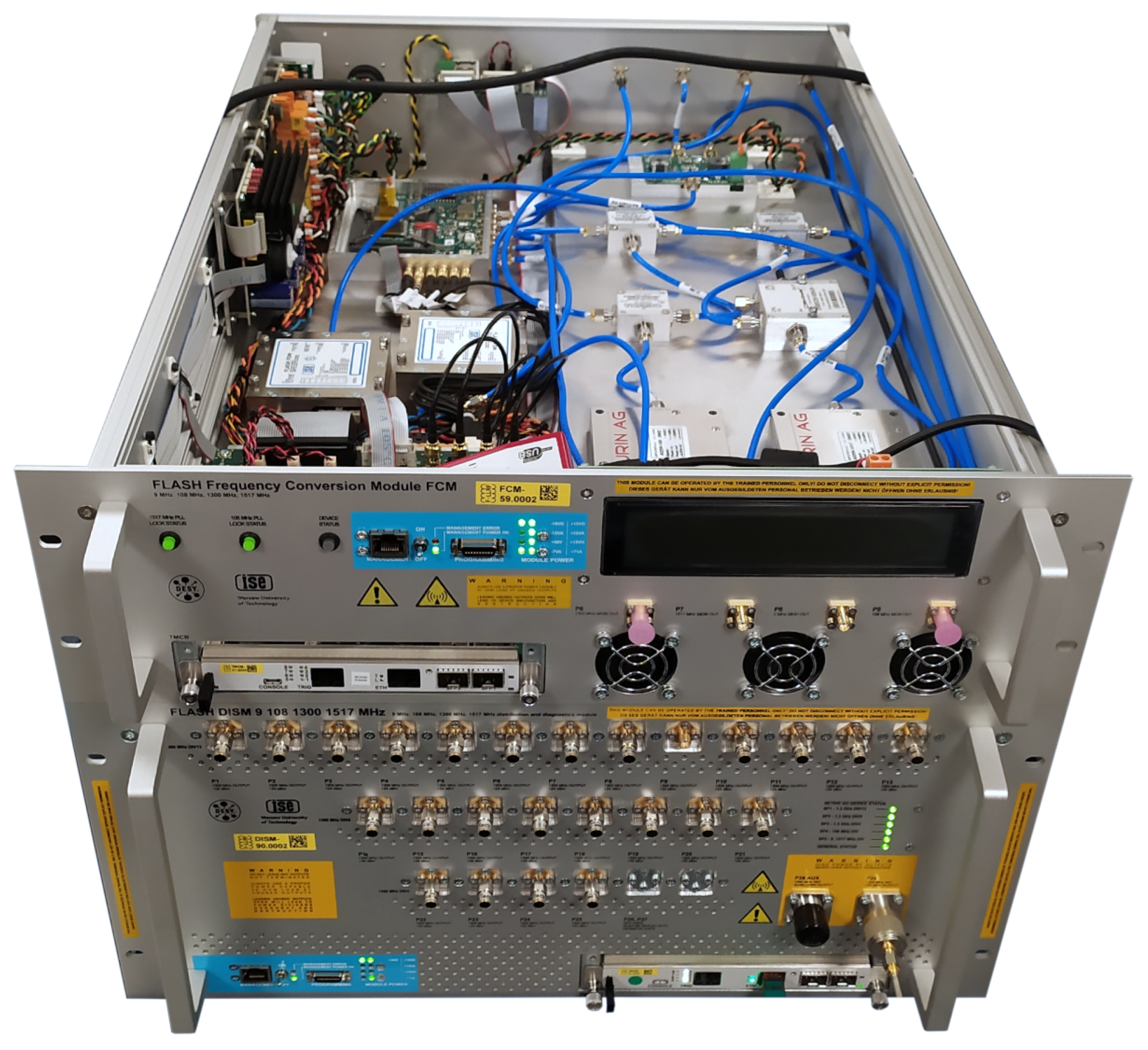
In the presented system, the MO synthesizes only the 1.3 GHz signal, and all the other frequency signals are then synthesized in the frequency conversion modules (FCM and also FCM-GUN), as shown in Figure 7 [19]. The FCM and FCM-GUN are based on custom-made frequency divider devices, and a new dual PLL that synthesizes 108 MHz and 1517 MHz signals. The new frequency divider, due to its simpler structure and absence of internal RF filters, is easier to implement in other applications. It offers the same functionality as the previous one in a smaller factor. It is also fitted with an input interlock circuit that turns off all the outputs in the absence of an input signal or its insufficient power level. The dual PLL uses an oven-compensated crystal oscillator (108 MHz) and a voltage-controlled oscillator (1517 MHz) to synthesize the required signals and improve their phase noise spectra. All output signals are in sync with the MO 1.3 GHz signal. The 9 MHz signal is conditioned by a 9 MHz buffer, which can drive a 50 Ohm load with 5 V p p signal, which corresponds to approx. +18 dBm. The photo of the FCM module is shown in Figure 8.
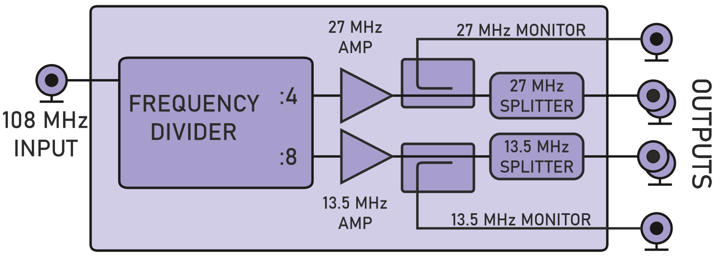
For an additional synthesis of 27 MHz and 13.5 MHz signals for the FLASH gun module, a separate frequency conversion module is used: the FCM GUN. Its main component is the frequency divider used in the FCM that divides the 108 MHz signal from the FCM to 27 MHz and 13.5 MHz outputs. These signals are then used for the synchronization of the gun. The block diagram of the FL-FCM-GUN module is shown in Figure 9, and the photo of the module installed in the FLASH facility in Figure 10.

8. Test Results

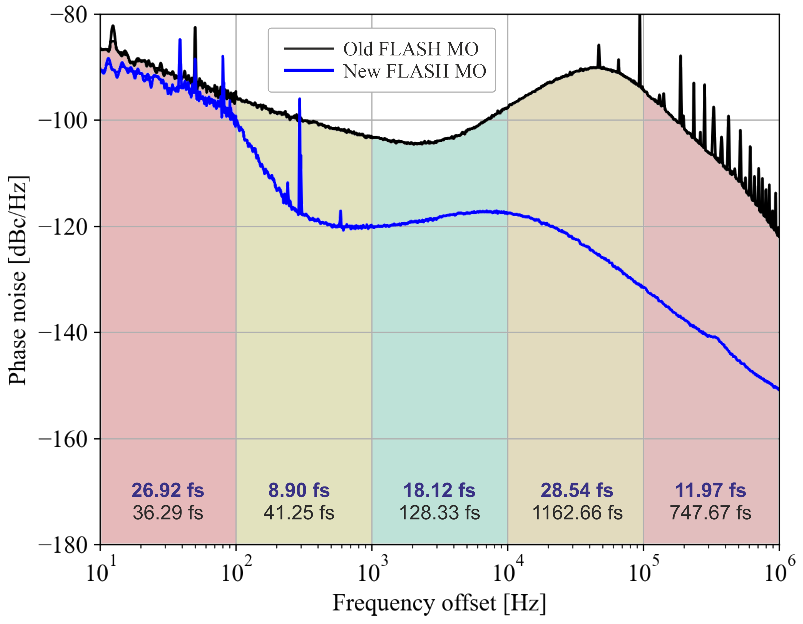
Tests were conducted at the Warsaw University of Technology, and then verified in the lab in DESY. The test stand used was prepared in a way that fully represents the final installation in FLASH. Except for the FCM GUN, all of the modules shown in Figure 1 were installed and connected. All of the modules were supplied with the same power supply as in the final system installation, and the same uTCA module was used for control and diagnostics. A high-quality R&S SMB100A was used as a 10 MHz reference for the MO module. During the design phase, the GPSDO was unavailable, yet this had no significant impact on the measured phase noise performance due to a narrow synchronization bandwidth of the first synthesis stage. However, GPSDO is necessary at the target location in order to meet the requirements of long-term frequency stability. The FL-MO1300, FL-DISM, and FL-FCM modules were connected as in the final installation in the FLASH facility and monitored remotely. All of the firmware development and diagnostic tests were performed remotely. All phase noise plots are presented in Figure 11, Figure 12 and Figure 13, grouped by signal frequencies [16]. For each of the mentioned plots, the integrated jitter is calculated and presented in Table 2 [16] in ranges from 10 Hz to 1 MHz and 1 kHz to 1 MHz of carrier offset, and also in selected bands in the plots, to show the noise band contribution.
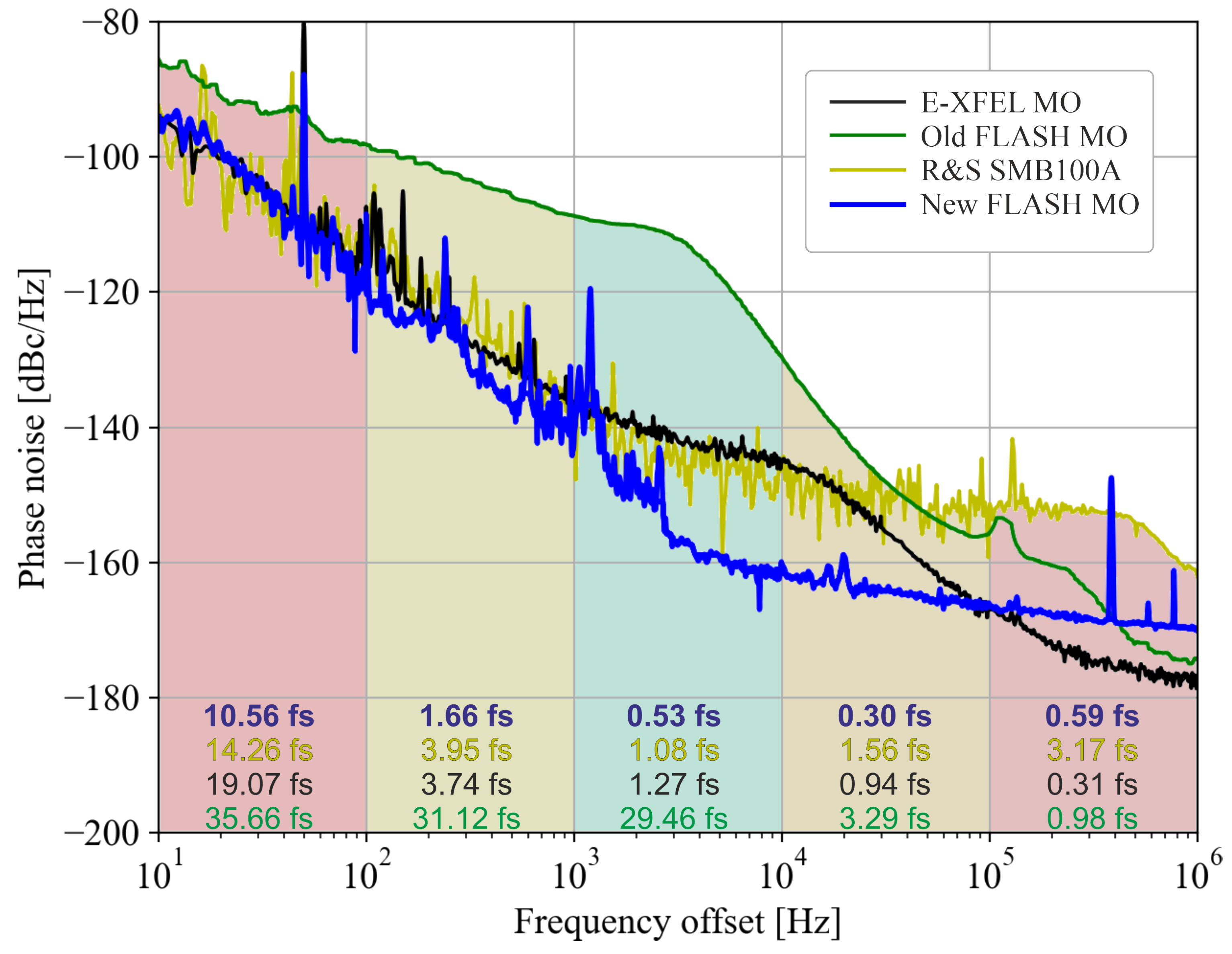
The 108 MHz signal jitter improvement is from 86.1 fs to 27.7 fs. The 1300 MHz signal jitter improvement is from 55.9 fs (old FLASH MO) to 10.7 fs in the new FLASH MO in the integration range from 10 Hz to 1 MHz, and 10.84 fs in the integration range from 10 Hz to 10 MHz. A phase noise PSD plot of the high-performance commercial R&S SMB100A synthesizer is presented for comparison. As presented in Figure 13, the most significant noise contribution is in the close to carrier band of 10 to 100 Hz. An optimization of spurious level is planned to reduce 1.3 GHz jitter below 10 fs. The shape of 1.517 GHz signal jitter differs significantly compared to 108 MHz and 1300 MHz plots. It is due to less demanding requirements for that signal and the way it is synthesized: via a typical PLL upconversion scheme, with a frequency divider in the feedback loop and an off-the-shelf voltage-controlled oscillator (VCO). The 1.517 GHz signal jitter improvement is from 1390.0 fs to 45.8 fs, which is thirty times better.

9. Conclusions

The new FLASH RF Reference Signal Generation and Distribution System is presented. It utilizes an improved frequency synthesis scheme and state-of-the-art components. The new system meets the requirements, and is successfully installed in the FLASH facility. The achieved phase noise results of the +47 dBm 1.3 GHz primary signal (10.7 fs in 10 Hz to 1 MHz range and less than 1 fs in 1 kHz to 1 MHz range) are outstanding—in terms of phase noise performance, it is better than one of the best commercially available RF generators, and than other solutions, like [10] (13.96 fs at signal power of +13.37 dBm). In cooperation with DESY, WUT has manufactured modules used in FLASH facility since 2022. A small-series production is taking place in cooperation with the industry for potential future users, like the E-XFEL, or other particle accelerator research facilities.

Author Contributions

Conceptualization, M.U. and B.G.; methodology, M.U. and B.G.; software, K.S.; validation, M.U., B.G., J.B. and H.P.; formal analysis, M.U., B.G., J.B. and H.P.; writing—original draft preparation, M.U.; writing—review and editing, M.U., B.G., K.C., J.B. and F.L.; visualization, T.O., A.Š., B.K., P.J. and D.K.; project administration, B.G.; funding acquisition, K.C. and J.B. All authors have read and agreed to the published version of the manuscript.

Funding

Research supported by the Polish Ministry of Science and Higher Education, founds for international co-financed projects for years 2020–2021, agreement 5083/DESY/2020/0.

Data Availability Statement

The data presented in this study are available on request from the corresponding author due to billateral cooperation agreements between WUT and DESY.

Conflicts of Interest

The authors declare no conflicts of interest.

References

  1. Beye, M.; Klumpp, S.; Faatz, B.; Hartl, I.; Lechner, C.; Ploenjes-Palm, E.; Schneidmiller, E.A.; Schreiber, S.; Tiedtke, K.; Treusch, R.; et al. FLASH2020+ Conceptual Design Report (CDR); Deutsches Elektronen-Synchrotron: Hamburg, Germany, 2020. [Google Scholar] [CrossRef]
  2. Faatz, B.; Plönjes, E.; Ackermann, S.; Agababyan, A.; Asgekar, V.; Ayvazyan, V.; Baark, S.; Baboi, N.; Balandin, V.; Von Bargen, N.; et al. Simultaneous operation of two soft X-ray free-electron lasers driven by one linear accelerator. New J. Phys. 2016, 18, 062002. [Google Scholar] [CrossRef]
  3. Branlard, J.; Chase, B.; Cullerton, F. Master Oscillator for Fermilab ILC Test Accelerator. In Proceedings of the LINAC 2006, Knoxville, TN, USA, 21–25 August 2006. [Google Scholar]
  4. Svensson, A.; Johansson, A. Master Oscillator for ESS, Design Description. Version 1.0; Lund University: Lund, Sweden, 2017. [Google Scholar]
  5. Zeng, R.; Persson, O.; Hassanzadegan, H.; Jurns, J.; Jensen, M.R.F.; Sunesson, A.; Strniša, K. Design of the Phase Reference Distribution System at ESS. In Proceedings of the 27th International Linear Accelerator Conference, Geneva, Switzerland, 31 August–5 September 2014. [Google Scholar]
  6. Lin, Z.; Du, Y.; Yang, J.; Huang, G.; Xu, Y.; Huang, W.; Tang, C. An active coaxial line phase reference distribution system. Nucl. Instruments Methods Phys. Res. Sect. A Accel. Spectrometers Detect. Assoc. Equip. 2020, 977, 164288. [Google Scholar] [CrossRef]
  7. Panofski, E.; Assmann, R.; Burkart, F.; Dorda, U.; Genovese, L.; Jafarinia, F.; Jaster-Merz, S.; Kellermeier, M.; Kuropka, W.; Lemery, F.; et al. Commissioning Results and Electron Beam Characterization with the S-Band Photoinjector at SINBAD-ARES. Instruments 2021, 5, 28. [Google Scholar] [CrossRef]
  8. Yamin, S. First Commissioning of the ARES Focusing System and its Possible Upgrade for Accelerator. Ph.D. Thesis, University of Hamburg, Hamburg, Germany, 2021. [Google Scholar]
  9. Min, C.-K.; Jung, S.H.; Kim, C.; Park, S.-J.; Kang, H.-S.; Ko, I.S. RF Timing Distribution and Laser Synchronization Commissioning of PAL-XFEL. In Proceedings of the 7th International Particle Accelerator Conference (IPAC’16), Busan, Republic of Korea, 8–13 May 2016. [Google Scholar] [CrossRef]
  10. Kim, C.; Park, S.J.; Min, C.K.; Hu, J.; Kim, S.H.; Joo, Y.; Heo, H.; Kim, D.E.; Lee, S.; Kang, H.S.; et al. Review of technical achievements in PAL-XFEL. AAPPS Bull. 2022, 32, 15. [Google Scholar] [CrossRef]
  11. Lin, Z.; Du, Y.; Yang, J.; Xu, Y.; Yan, L.; Huang, W.; Tang, C.; Huang, G.; Du, Q.; Doolittle, L.; et al. Development of sub-100 femtosecond timing and synchronization system. Rev. Sci. Instruments 2018, 89, 014701. [Google Scholar] [CrossRef] [PubMed]
  12. Cicek, E.; Fang, Z.; Fukui, Y.; Futatsukawa, K.; Hirane, T.; Sato, Y.; Shinozaki, S. A Recent Upgrade on Phase Drift Compensation System for a Stable Beam Injection at J-PARC Linac. In Proceedings of the 12th International Particle Accelerator Conference (IPAC’21), Campinas, SP, Brazil, 24–28 May 2021. [Google Scholar] [CrossRef]
  13. Liu, N.; Miura, T.; Matsumoto, T.; Kobayashi, T.; Iida, N.; Qiu, F.; Michizono, S.; Arakawa, D.; Katagiri, H.; Yano, Y.; et al. Phase drift compensation between injector linac master oscillator and ring master oscillator for stable beam injection at SuperKEKB. Phys. Rev. Accel. Beams 2019, 22, 072002. [Google Scholar] [CrossRef]
  14. Sydlo, C.; Felber, M.; Gerth, C.; Kozak, T.; Lamb, T.; Müller, J.; Schlarb, H.; Zummack, F. Femtosecond Optical Synchronization System for the European XFEL. In Proceedings of the 8th International Particle Accelerator Conference, 2017, Copenhagen, Denmark, 14–19 May 2017. [Google Scholar] [CrossRef]
  15. Young, A. Low Phase-Noise, Low Jitter Master Oscillator for the LCLS Cavity BPM System. In Proceedings of the Particle Accelerator Conference (PAC 09), Vancouver, BC, Canada, 4–8 May 2009. [Google Scholar]
  16. Urbański, M. Development of Phase Reference Distribution Systems of Linear Particle Accelerators with Femtosecond Stability. Ph.D. Thesis, Warsaw University of Technology, Warsaw, Poland, 2023. [Google Scholar]
  17. Gąsowski, B.; Urbański, M.; Czuba, K.; Branlard, J.; Pryschelski, H.; Ludwig, F. Concept of Master Oscillator Upgrade for FLASH. In Proceedings of the 2020 23rd International Microwave and Radar Conference (MIKON), Warsaw, Poland, 5–8 October 2020; pp. 165–168. [Google Scholar] [CrossRef]
  18. The Distributed Object-Oriented Control System Framework (DOOCS). Available online: https://doocs-web.desy.de (accessed on 13 November 2024).
  19. Urbański, M.; Gąsowski, B.; Šerlat, A.; Kola, B.; Jatczak, P.; Owczarek, T.; Czuba, K.M.; Branlard, J.; Pryschelski, H.; Schulz, K.; et al. FLASH2020+ RF Reference Generation System Upgrade Status. Presentation at the Low-Level RF Workshop 2022, Brugg-Windisch, Switzerland, 9–13 October 2022; Available online: https://indico.psi.ch/event/12911/contributions/38390/ (accessed on 13 November 2024).
  20. Viti, M.; Czwalinna, M.K.; Dinter, H.; Gerth, C.; Przygoda, K.; Rybaniec, R.; Schlarb, H. The Bunch Arrival Time Monitor at FLASH and European XFEL. In Proceedings of the 16th International Conference on Accelerator and Large Experimental Physics Control Systems (ICALEPCS 2017), Barcelona, Spain, 8–13 October 2017. [Google Scholar] [CrossRef]
  21. Hati, A.; Craig, N.; Howe, D. Vibration-Induced PM Noise in Oscillators and Its Suppression. In Aerial Vehicles; InTech: London, UK, 2009. [Google Scholar] [CrossRef]
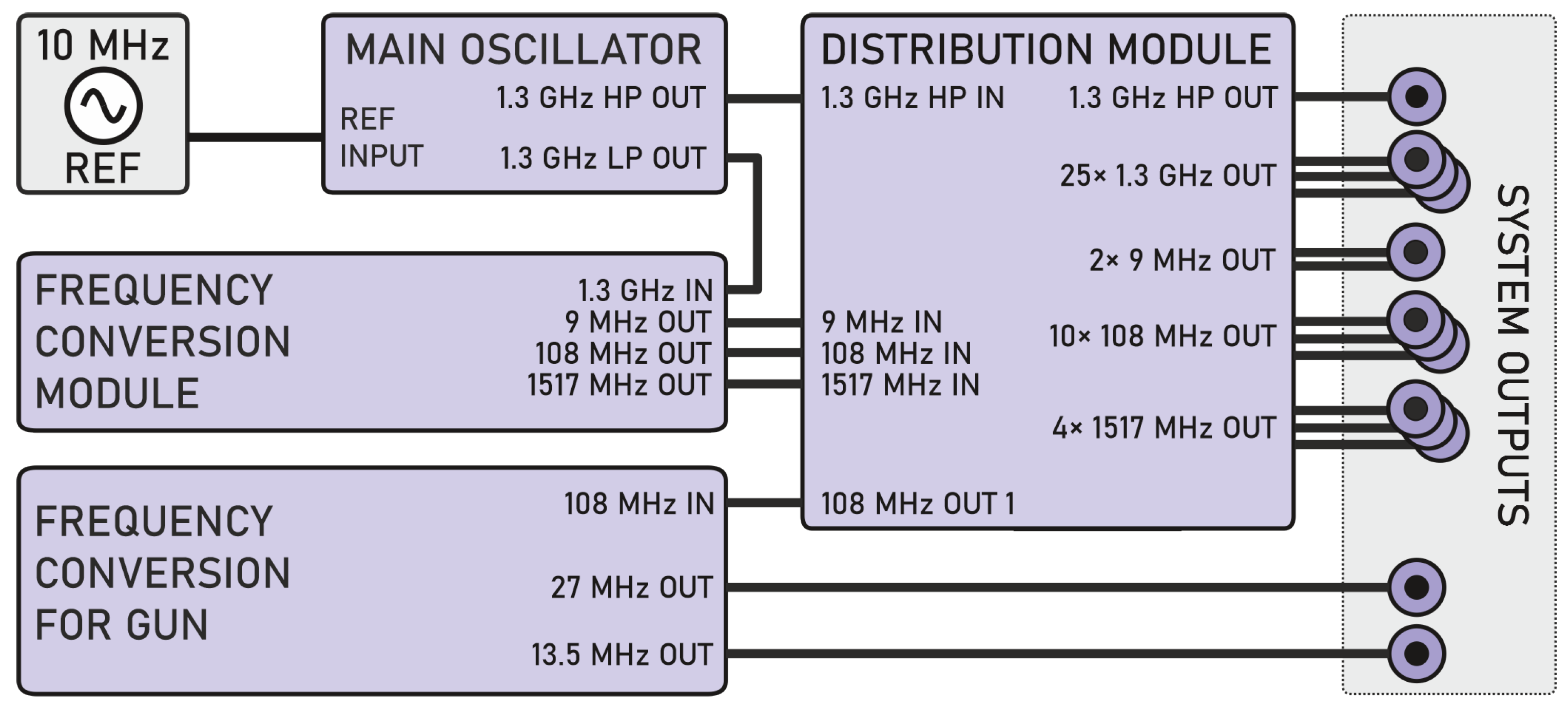
Figure 1. The upgraded RF generation and distribution system for FLASH.
Electronics 14 00173 g001
Figure 2. The new FLASH MO block diagram.
Electronics 14 00173 g002
Figure 3. Phase noise PSD plots for selected FL-MO1300 components and their cascades, with total jitter calculated in selected offset frequency bands.
Electronics 14 00173 g003
Figure 4. The new FLASH MO module front panel view and internal design view.
Electronics 14 00173 g004
Figure 5. Block diagram of the FL-DISM distribution module.
Electronics 14 00173 g005
Figure 6. The new FLASH DISM module internal view.
Electronics 14 00173 g006
Figure 7. FL-FCM block diagram.
Electronics 14 00173 g007
Figure 8. FL-FCM module photo, during tests with FL-DISM.
Electronics 14 00173 g008
Figure 9. Frequency conversion for GUN, the FCM GUN block diagram.
Electronics 14 00173 g009
Figure 10. Frequency conversion for GUN: FL-FCM-GUN module photo, installed in the rack in the FLASH facility.
Electronics 14 00173 g010
Figure 11. Comparison of phase noise performance at FLASH at 108.33 MHz, with total jitter calculated in selected offset frequency bands.
Electronics 14 00173 g011
Figure 12. Comparison of phase noise performance at FLASH at 1517 MHz, with total jitter calculated in selected offset frequency bands.
Electronics 14 00173 g012
Figure 13. Comparison of phase noise performance at 1.3 GHz, with total jitter calculated in selected offset frequency bands.
Electronics 14 00173 g013
Table 1. FLASH MO main parameters.
1300 MHz main reference signal
Output frequency (H)1300 MHz
Number of outputs (H)25 low power, 1 high power
Power level at high-power (HP) output (H)+44 dBm approx.
Power levels at low-power (LP) outputs (H)+20 to +26 dBm
Phase stability (jitter) (S)less than 10 fs RMS, (10 Hz–1 MHz)
Frequency stability (H)better than 10 12 (Allan deviation for measurement time of hours days)
Amplitude stability (H)better than 0.1%
108 MHz reference signal
Output frequency (H)1300 MHz · 1 12 = 108.(3) MHz
Number of outputs (H)10
Output power levels (H)+10 to +23 dBm
1517 MHz reference signal
Output frequency (H)1300 MHz · 7 6 = 1516.(6) MHz
Number of outputs (H)4
Output power levels (H)+17 dBm
9 MHz reference signal
Output frequency (H)1300 MHz · 1 144 = 9.02(7) MHz
Number of outputs (H)2 (signal output and monitoring output)
Output power levels (H) 5 V p p at 50 Ohm load, approx. +18 dBm
Table 2. Integrated jitter for selected MO modules.
Integrated jitter from 10 Hz to 1 MHz carrier offset
 Old FLASH MOE-XFEL MONew FLASH MO
108 MHz86.1 fsnot synthesized27.8 fs
1300 MHz55.9 fs19.5 fs10.7 fs
1517 MHz1390 fsnot synthesized45.8 fs
Integrated jitter from 1 kHz to 1 MHz carrier offset
 Old FLASH MOE-XFEL MONew FLASH MO
108 MHz6.3 fsnot synthesized4.4 fs
1300 MHz29.7 fs1.6 fs0.8 fs
1517 MHz1390 fsnot synthesized35.9 fs
Disclaimer/Publisher’s Note: The statements, opinions and data contained in all publications are solely those of the individual author(s) and contributor(s) and not of MDPI and/or the editor(s). MDPI and/or the editor(s) disclaim responsibility for any injury to people or property resulting from any ideas, methods, instructions or products referred to in the content.