
A Low-Reflection Tuning Strategy for Three-Stub Waveguides


 and
and
Abstract
1. Introduction
2. Study on Input Impedance of Three-Stub Waveguide
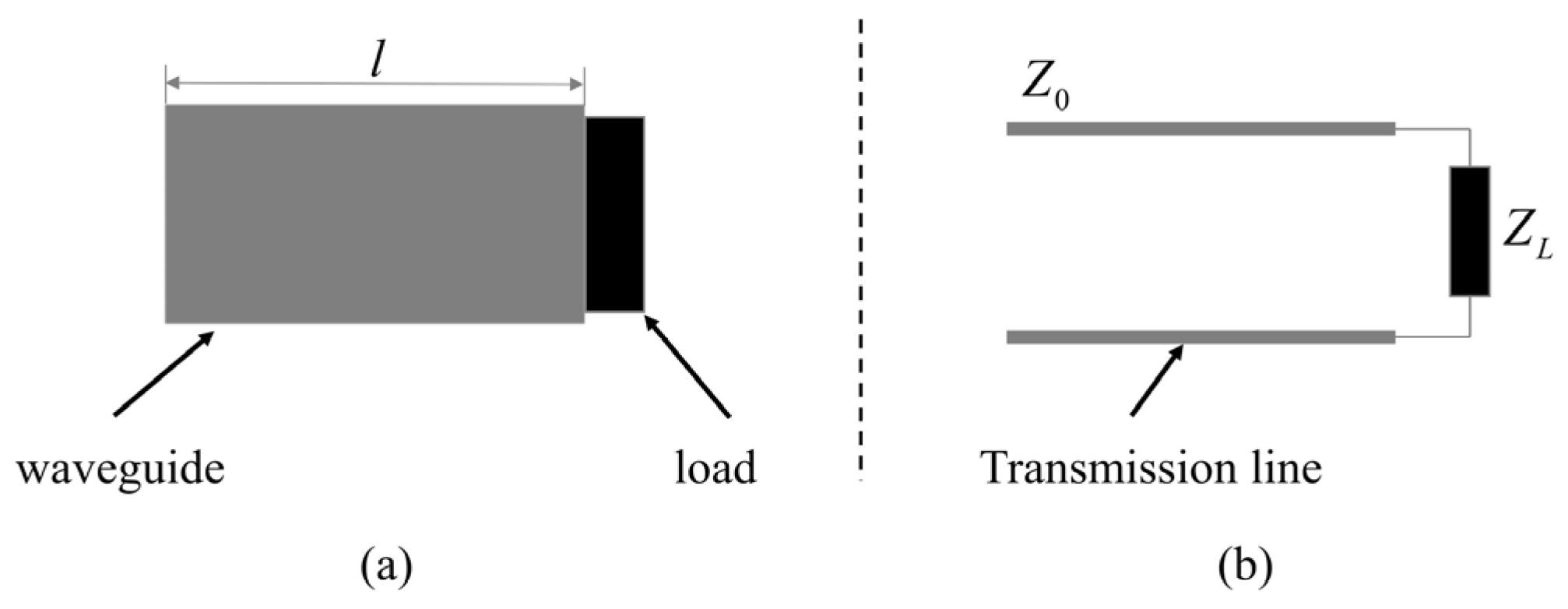
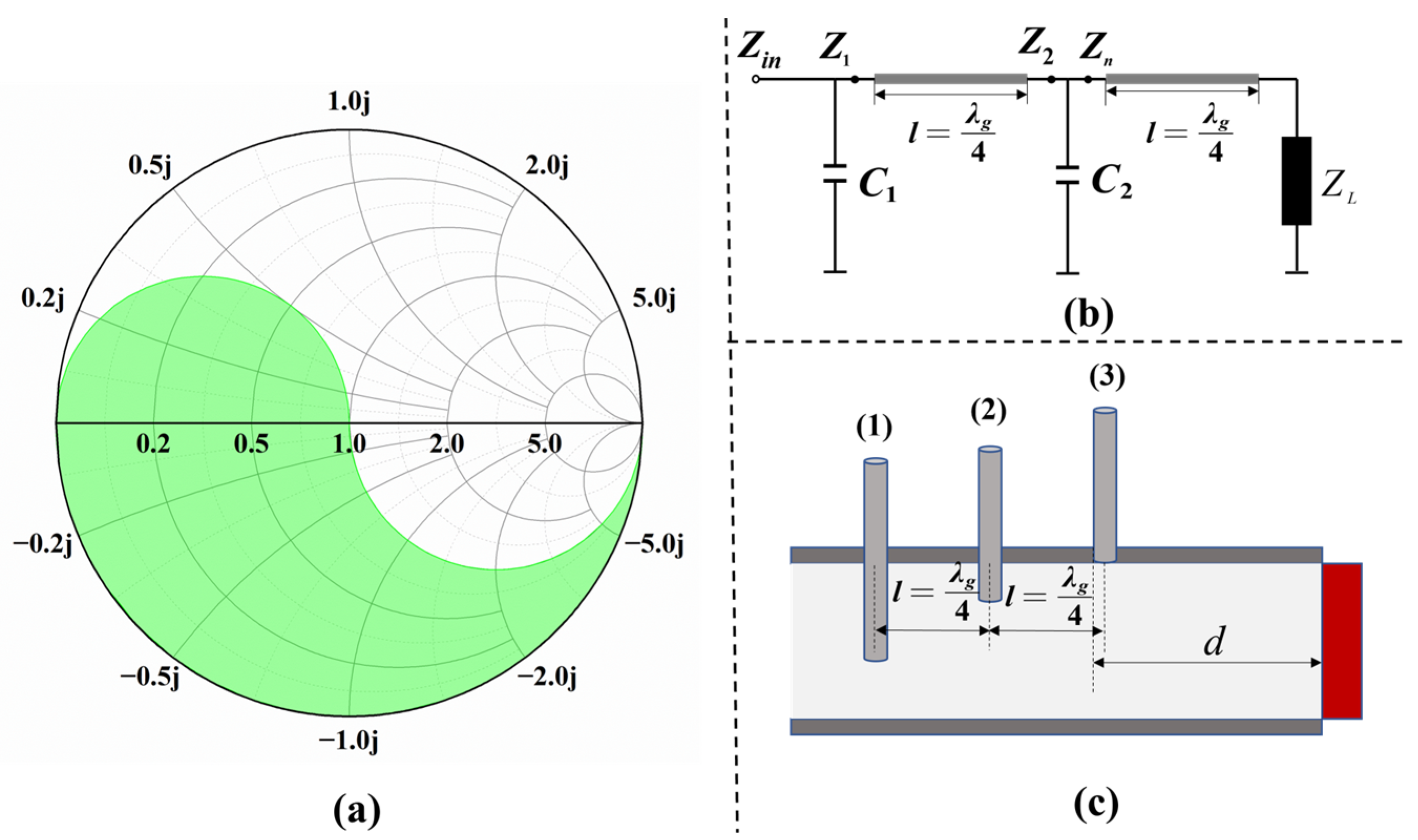
2.1. Input Impedance of Rectangular Waveguide
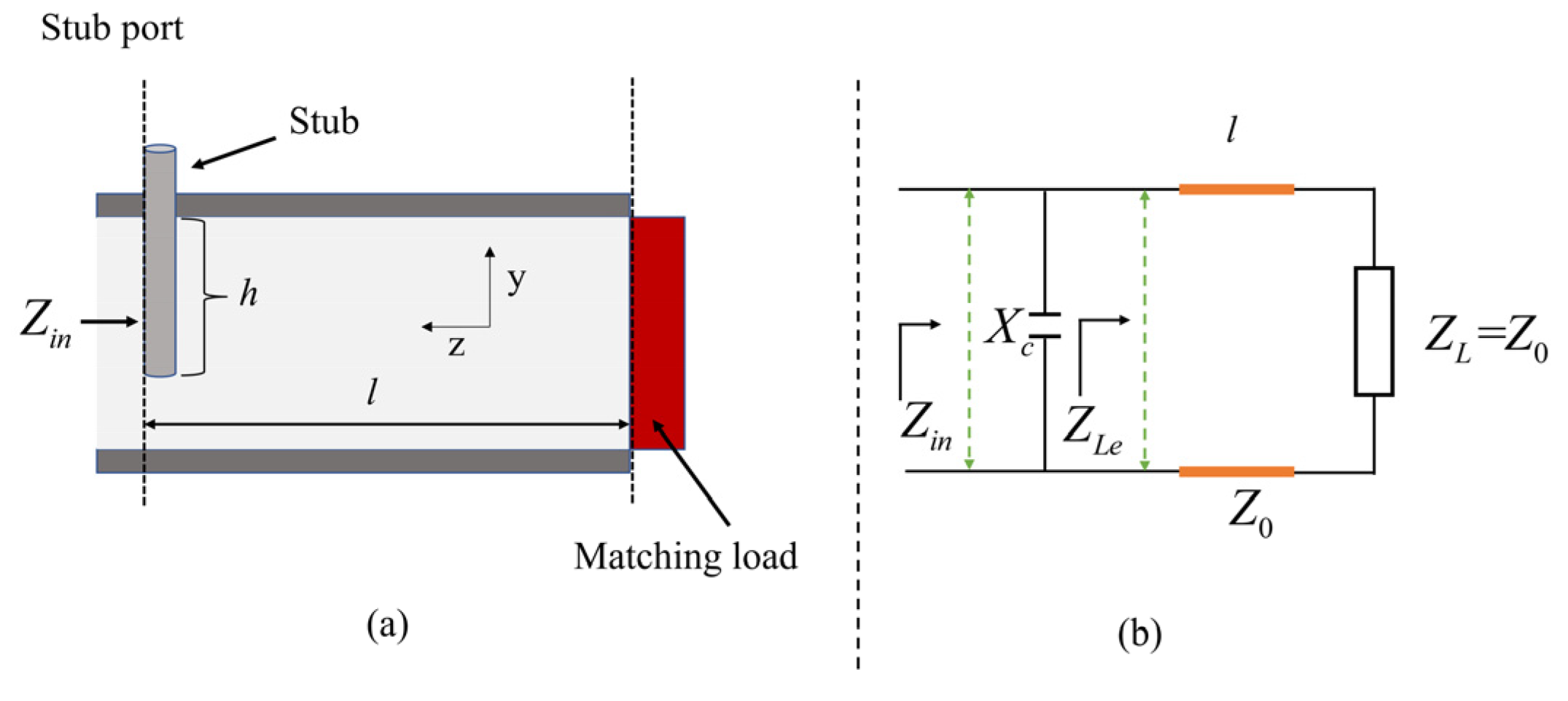
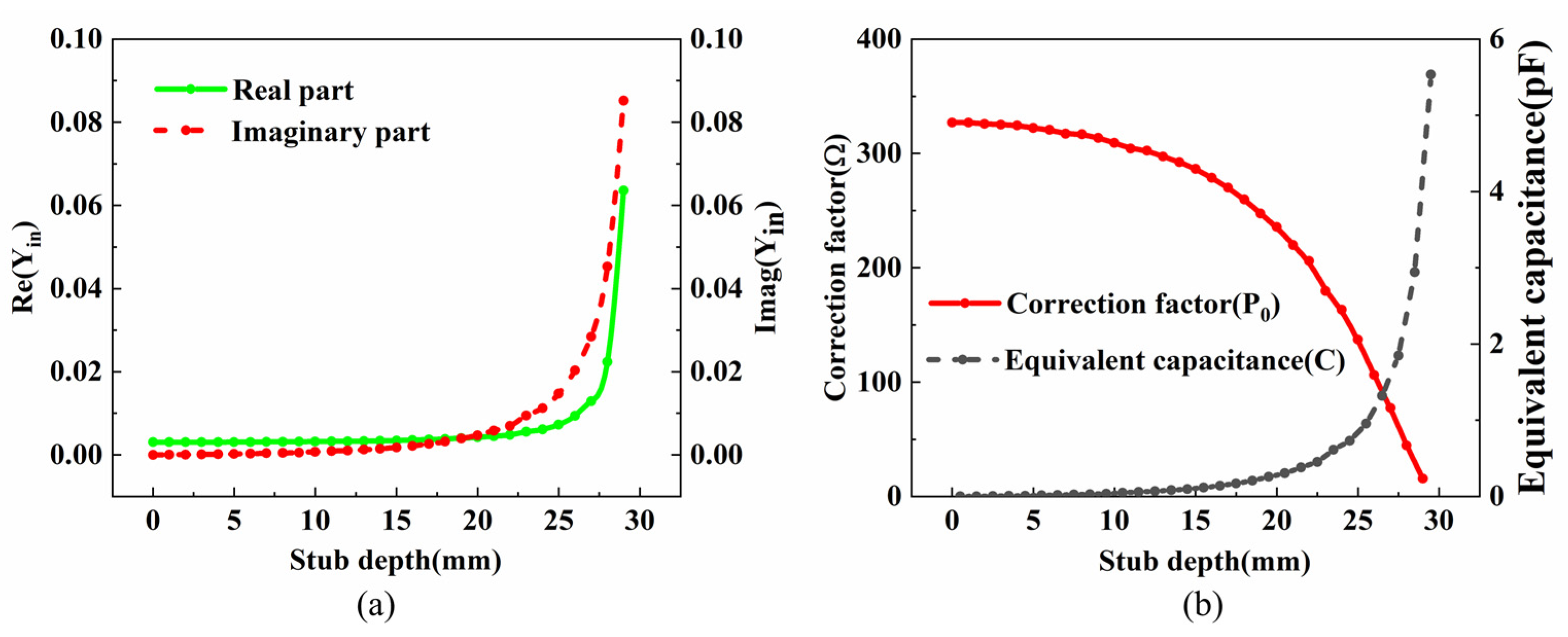
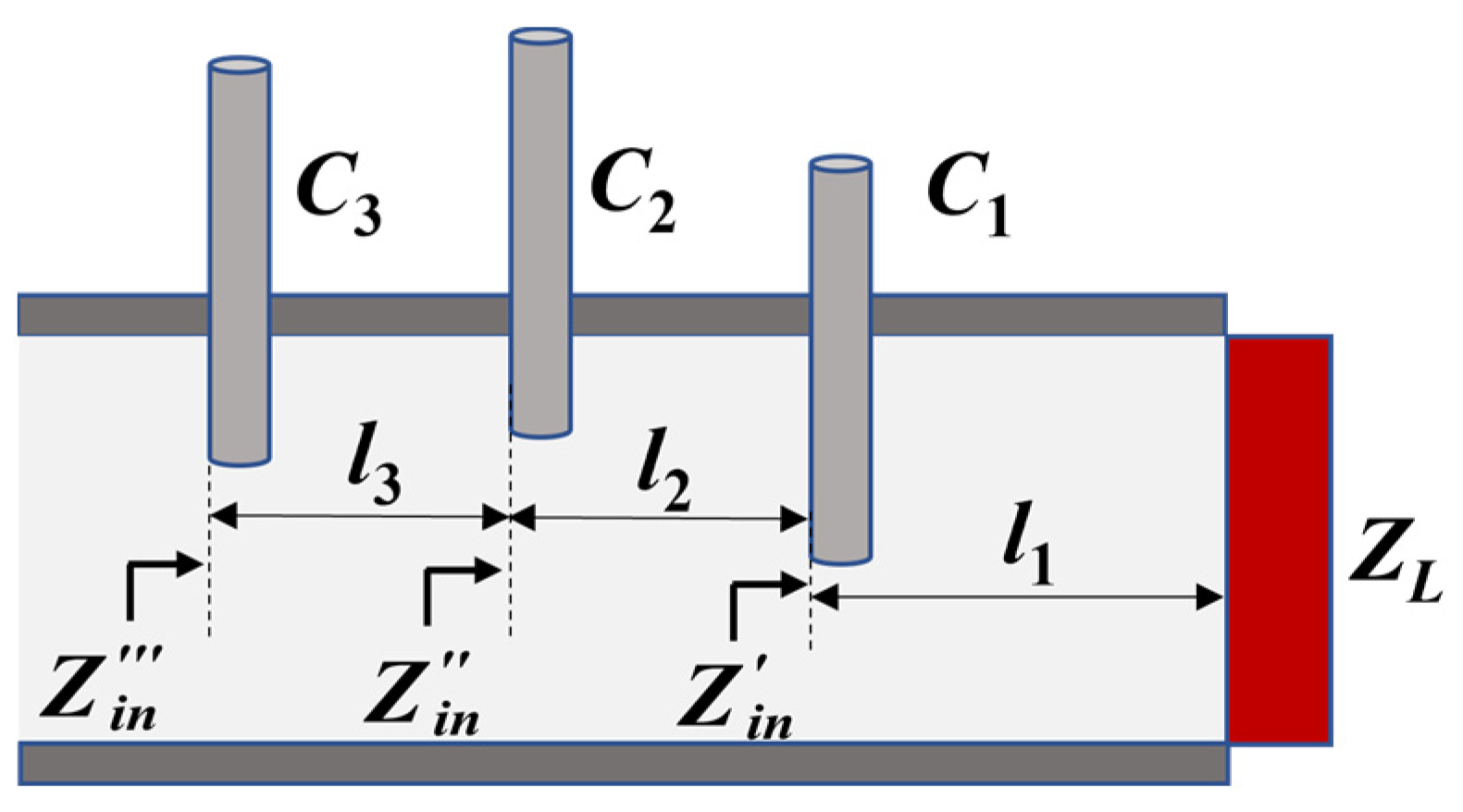
2.2. An Improved Method Based on Input Impedance of Three-Stub Waveguide
3. A Low-Reflection Tuning Strategy
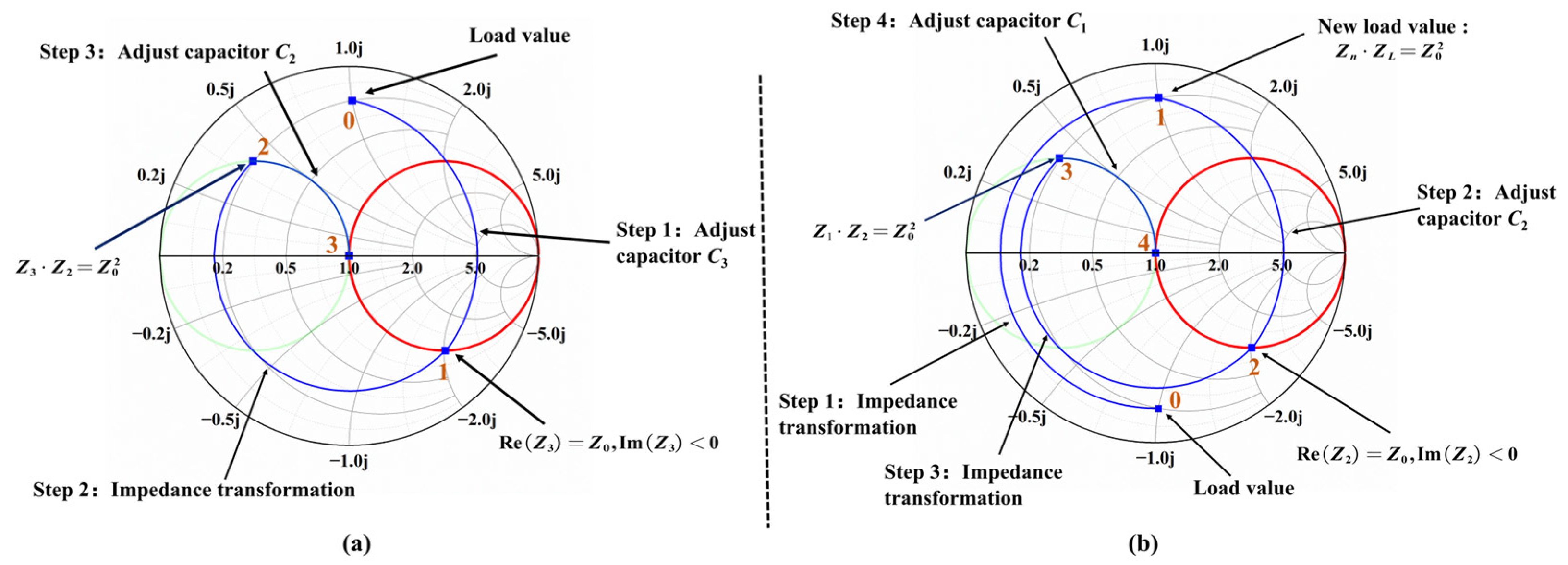
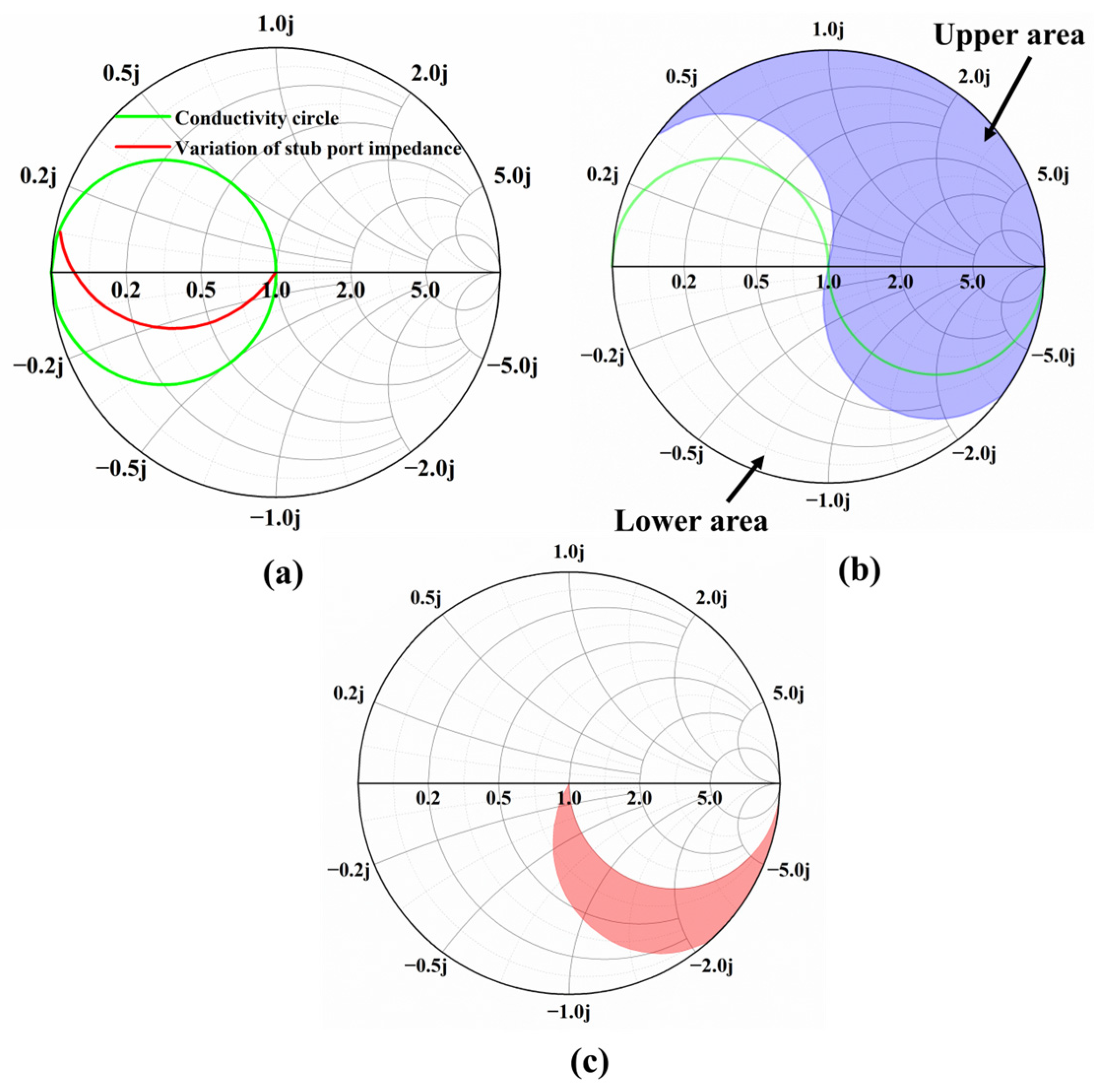
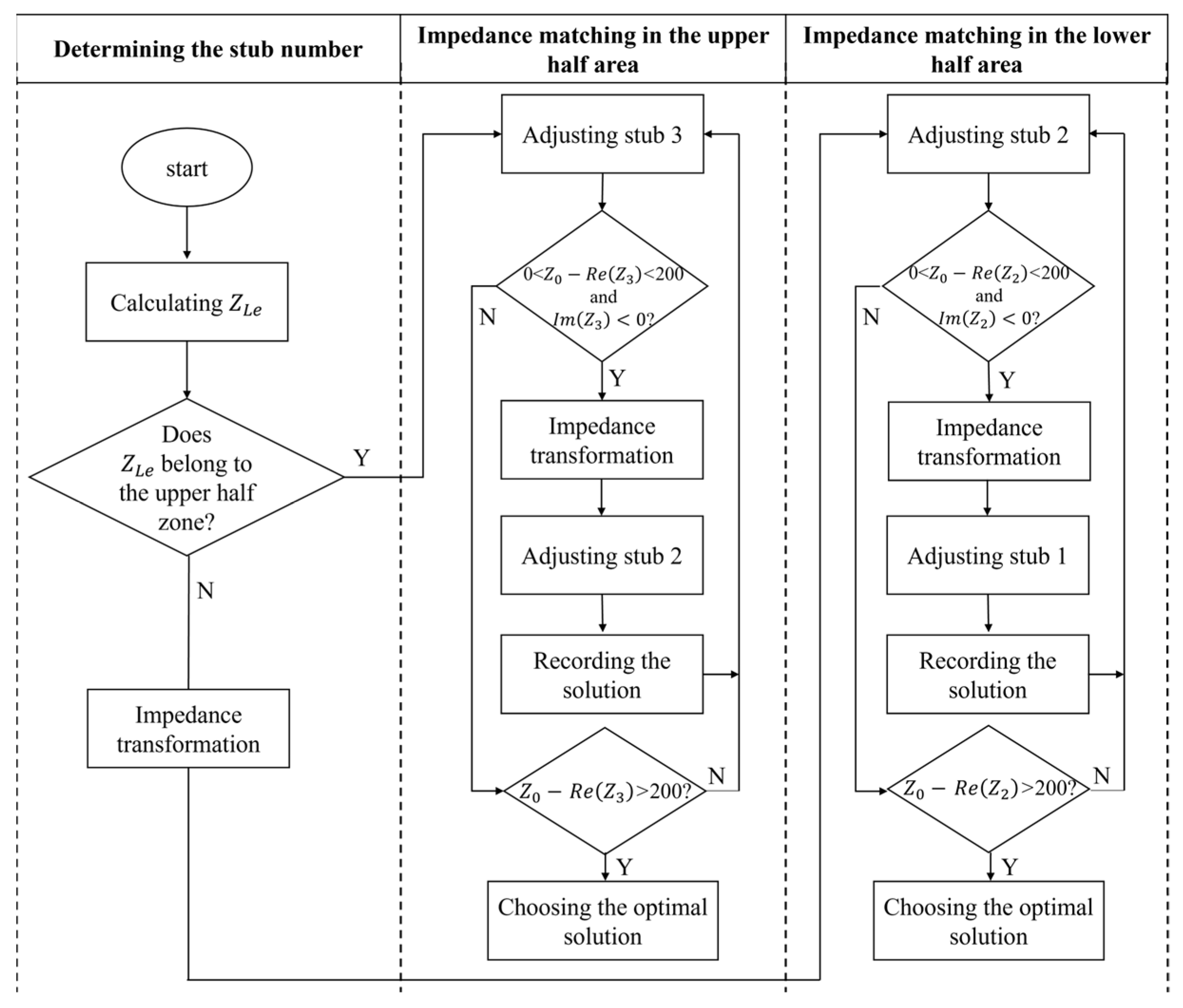
3.1. Impedance Matching Algorithm
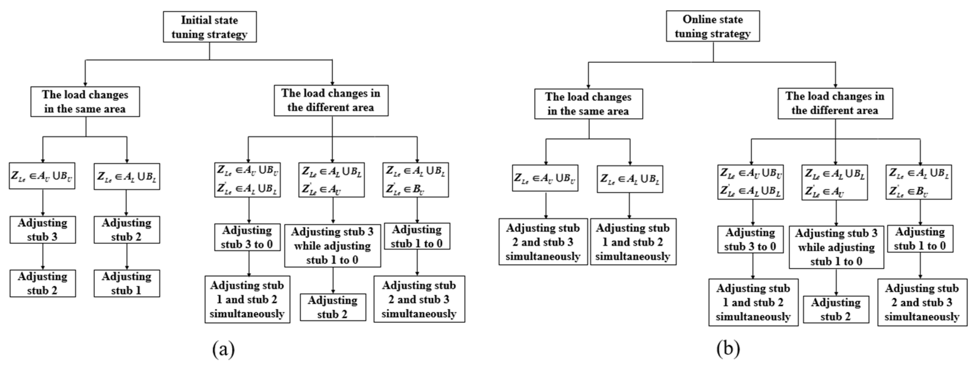
3.2. Low-Reflection Tuning Strategy
- a.
- Initial state tuning strategy
- b.
- Online state tuning strategy
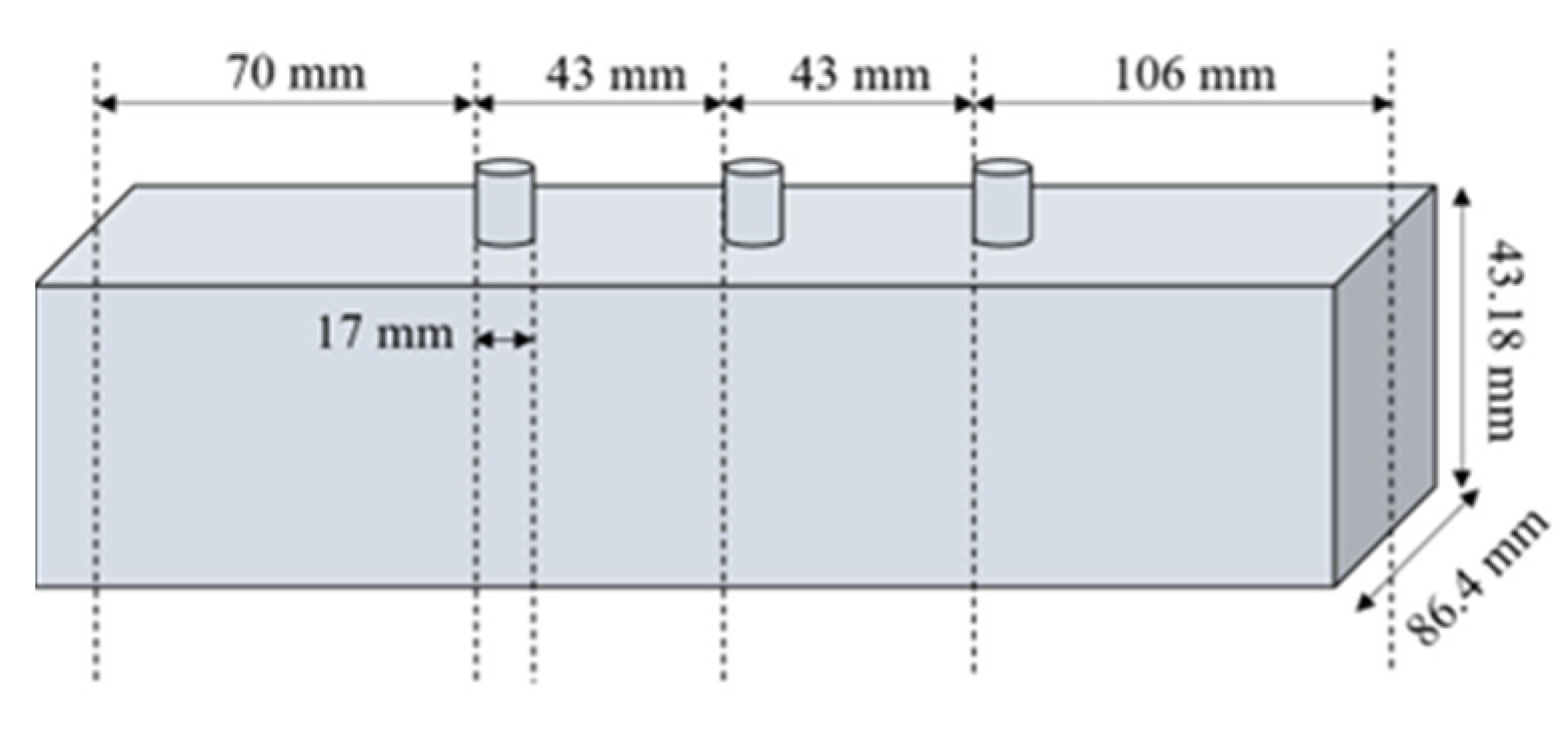
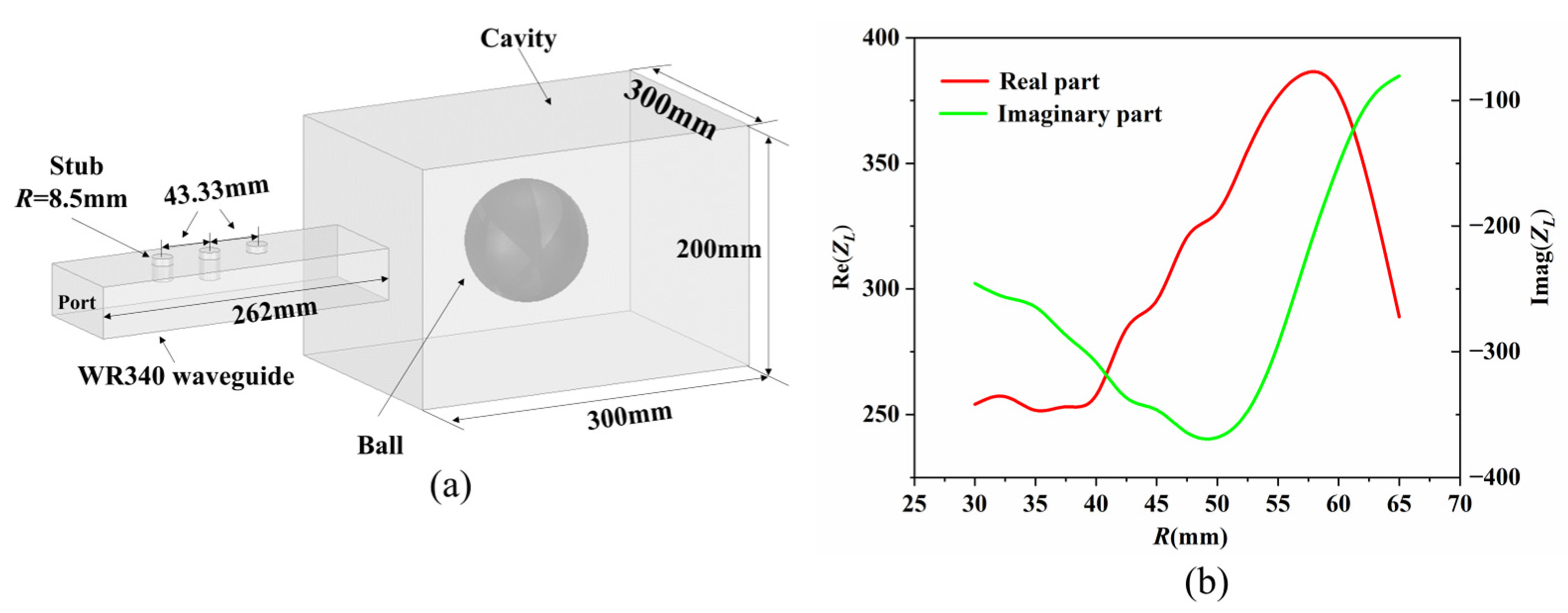
4. Experimental Verification and Discussion
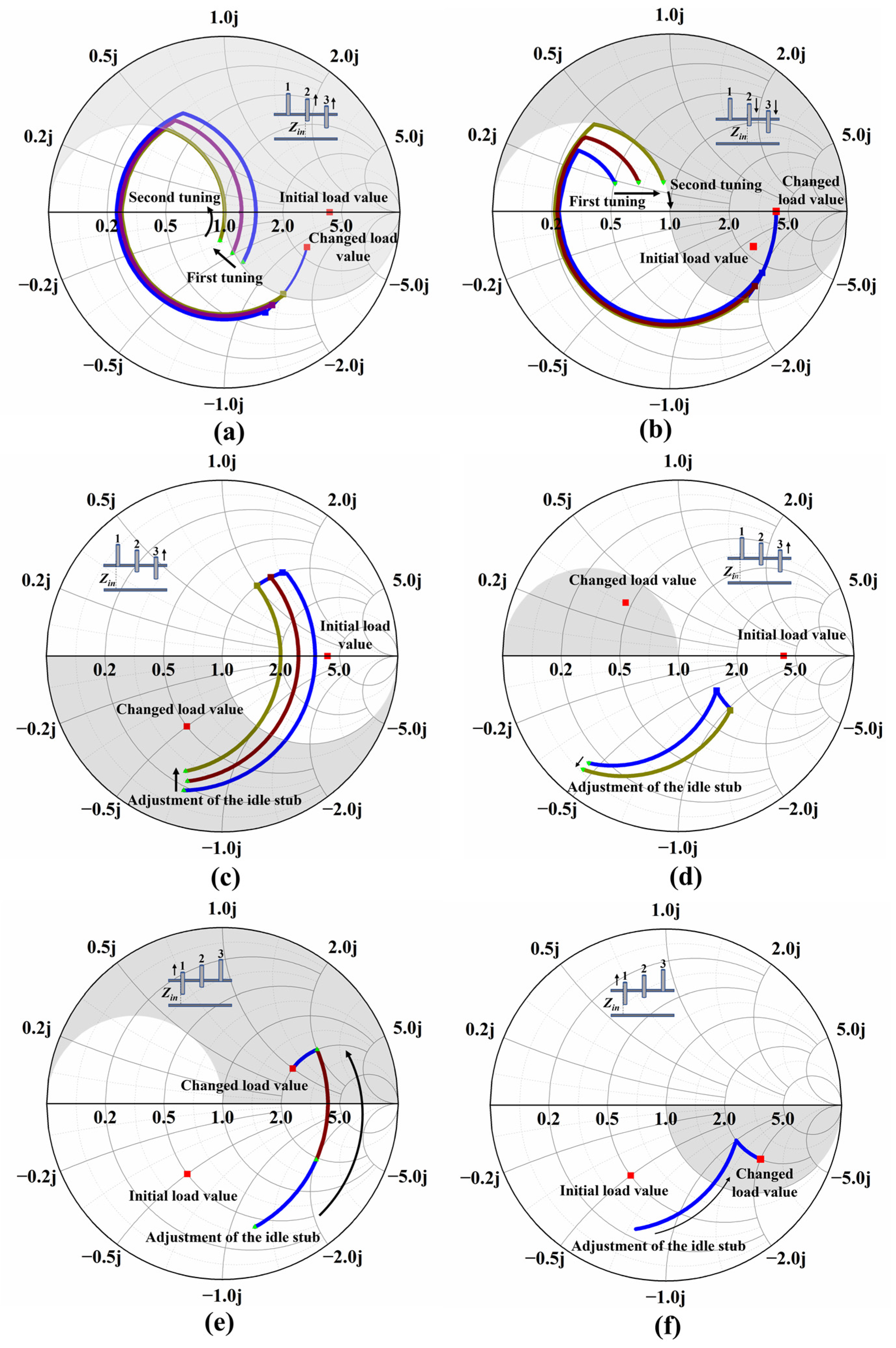
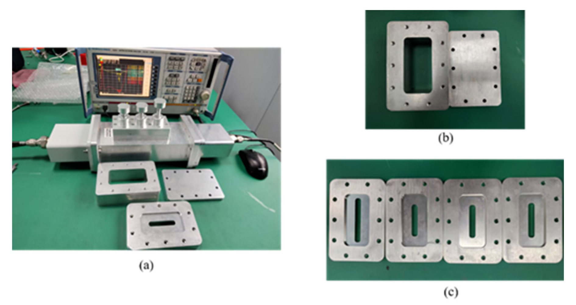
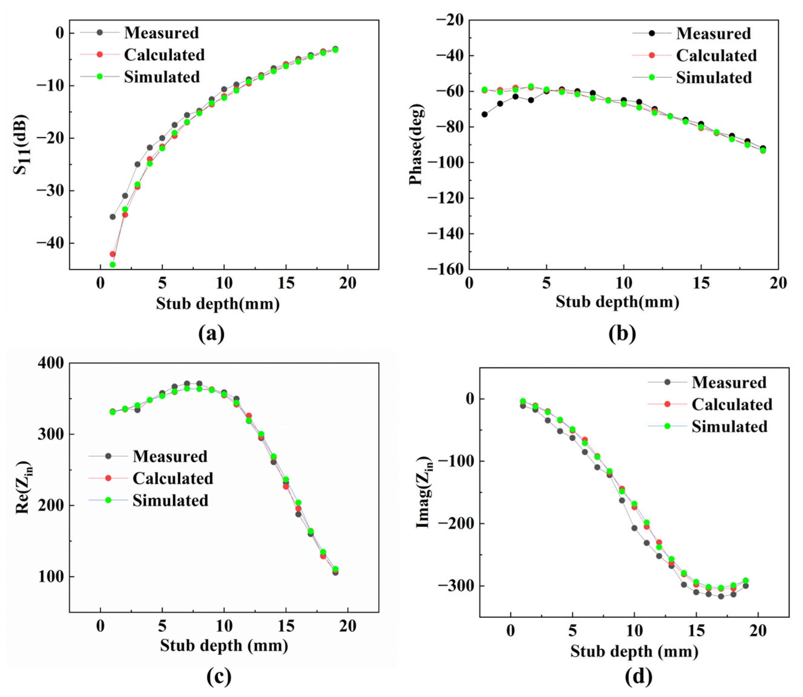
4.1. Validation of Matching Algorithms
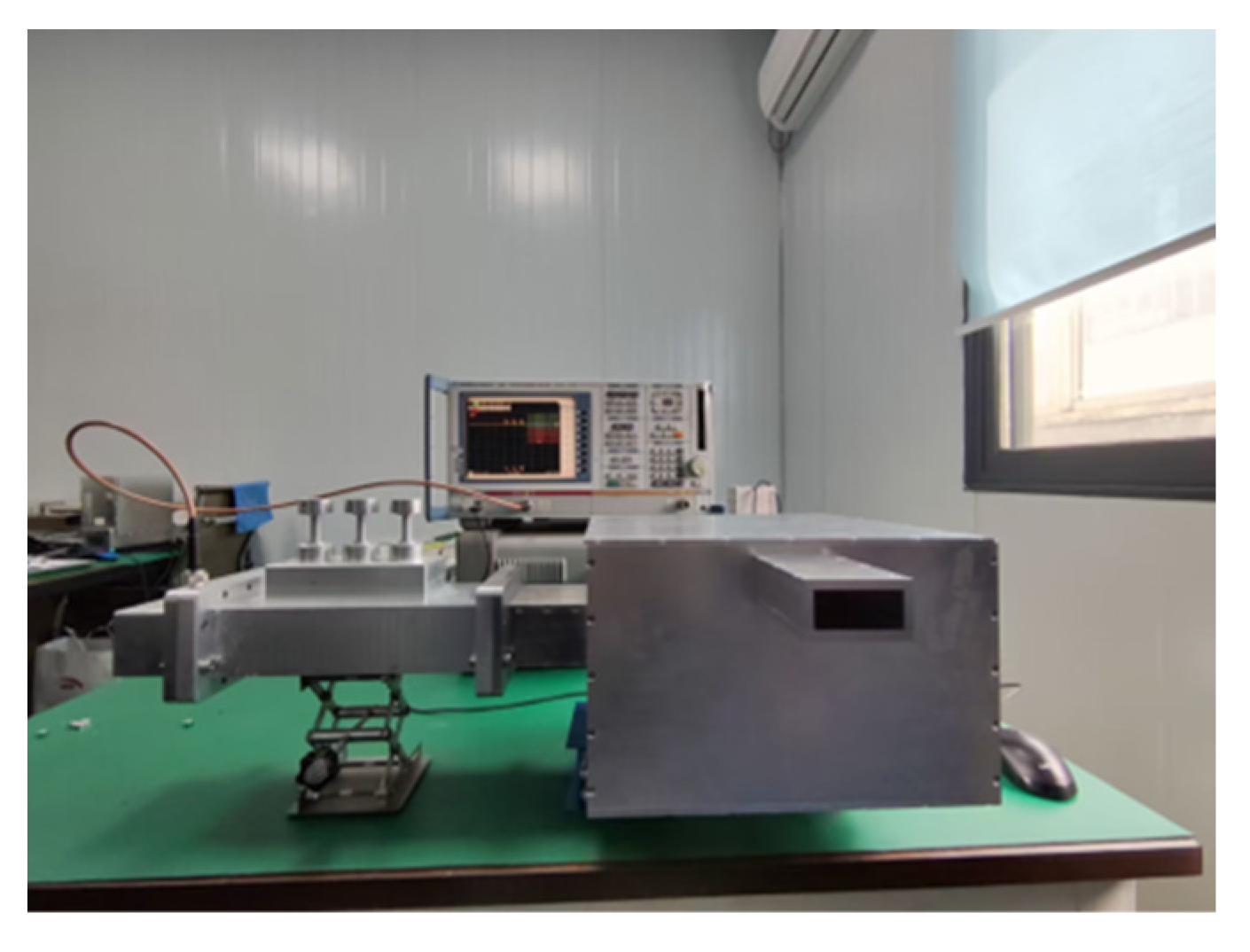
4.2. Validation of the Tuning Strategy
5. Conclusions
Author Contributions
Funding
Data Availability Statement
Conflicts of Interest
References
- Nakano, S.; Kim, J.-H.; Hwang, T.; Kasada, R.; Nakamichi, M. Dissolution and recovery of beryllium from beryl using a novel wet process with microwave heating. Nucl. Mater. Energy 2022, 30, 101113. [Google Scholar] [CrossRef]
- Jung, S.; Kwak, J.H.; Han, S.M. Guided-wavelength-controlled dynamic microwave heating in a near-cutoff waveguide. Appl. Therm. Eng. 2021, 188, 116630. [Google Scholar] [CrossRef]
- Chi, C.; Fu, W.; Zhang, C.; Lu, D.; Han, M.; Yan, Y. Dual-Frequency Microwave Plasma Source Based on Microwave Coaxial Transmission Line. Appl. Sci. 2021, 11, 9873. [Google Scholar] [CrossRef]
- Norrawit, T.; Akira, Y.; Nobuya, H. Surface sterilization using LF-microwave hybrid plasma. Jpn. J. Appl. Phys. 2021, 60, SAAE01. [Google Scholar]
- Shevelev, O.; Petrova, M.; Smolensky, A.; Osmonov, B.; Toimatov, S.; Kharybina, T.; Karbainov, S.; Ovchinnikov, L.; Vesnin, S.; Tarakanov, A.; et al. Using medical microwave radiometry for brain temperature measurements. Drug Discov. Today 2022, 27, 881–889. [Google Scholar] [CrossRef]
- Wang, Z.; Yu, C.; Huang, H.; Guo, W.; Yu, J.; Qiu, J. Carbon-enabled microwave chemistry: From interaction mechanisms to nanomaterial manufacturing. Nano Energy 2021, 85, 106027. [Google Scholar] [CrossRef]
- Bilik, V.; Bezek, J. Investigation of High-Power Limits of Stub Tuners by Means of Electromagnetic Simulation. In Proceedings of the 2008 14th Conference on Microwave Techniques, Prague, Czech Republic, 23–24 April 2008; pp. 1–4. [Google Scholar]
- Bilik, V.; Bezek, J. High power limits of waveguide stub tuners. J. Microw. Power Electromagn. Energy 2010, 44, 178–186. [Google Scholar] [CrossRef]
- Zhuang, Q.; Yan, F.; Jiang, Z.; Liu, M.; Xiong, Z.; Yan, C. Study and design of a contracting waveguide phase shifter for s-band high-power microwave applications. In Proceedings of the 2019 IEEE 2nd International Conference on Electronics Technology (ICET), Chengdu, China, 10–13 May 2019; pp. 162–165. [Google Scholar]
- Duan, Y.; Fu, Y.; Shi, Y.; Pang, H.; Huang, L. T-ZnOw/FCIPs with vertical-orientated structure achieving temperature-stable broadband microwave absorption. Appl. Surf. Sci. 2022, 613, 155988. [Google Scholar] [CrossRef]
- Livshits, P.; Gurfinkel, M.; Fefer, Y. VLSI MOSFETs lifetime reduction caused by impedance mismatch. Microelectron. Eng. 2011, 88, 28–31. [Google Scholar] [CrossRef]
- Ishibashi, K.; Sawado, E. Three-dimensional analysis of electromagnetic fields in rectangular waveguides by the boundary integral equation method. IEEE Trans. Microw. Theory Techn. 1990, 38, 1300–1308. [Google Scholar] [CrossRef]
- Yang, N.; Huang, Y. Analysis of a post with arbitrary cross-section and height in a rectangular waveguide. IEE Proc. Part. H. Microwaves Antennas Propag. 1991, 138, 475–480. [Google Scholar]
- Kocabas, S.E.; Veronis, G.; Miller, D.A.B.; Fan, S. Transmission Line and Equivalent Circuit Models for Plasmonic Waveguide Components. IEEE J. Quantum Electron. 2008, 14, 1462–1472. [Google Scholar] [CrossRef]
- Wyslouzil, W.; VanKoughnett, A.L. Automated Matching of Resonant Microwave Heating Systems. J. Microw. Power Electromagn. Energy 1973, 8, 89–100. [Google Scholar] [CrossRef]
- Mallorqui, J.J.; Aguasca, A.; Cardama, A.; Pagès, R.; Haro, J. Application of the conjugate gradient method to a self-matching network for industrial microwave heating antennas. In Proceedings of the IEEE Antennas and Propagation Society International Symposium, Orlando, FL, USA, 11–16 July 1999; pp. 978–981. [Google Scholar]
- Bandler, J.W.; Cheng, Q.S.; Dakroury, S.A. Space Mapping: The State of the Art. IEEE Trans. Microw. Theory Techn. 2004, 52, 337–361. [Google Scholar] [CrossRef]
- Koziel, S.; Bandler, J.W. Space Mapping with Multiple Coarse Models for Optimization of Microwave Components. IEEE Microw. Wireless Compon. Lett. 2008, 18, 1–3. [Google Scholar] [CrossRef]
- Cheng, Q.S.; Bandler, J.W.; Nikolova, N.K.; Koziel, S. A Statistical Input Space Mapping Approach for Accommodating Modeling Residuals. In Proceedings of the 2013 IEEE MTT-S International Microwave Symposium Digest (MTT), Seattle, WA, USA, 2–7 June 2013; pp. 1–3. [Google Scholar]
- Parro, V.C.; Pait, F.M. An automatic impedance matching system for a multi point power delivery continuous industrial microwave oven. In Proceedings of the 2004 IEEE International Conference on Control Applications, Taipei, Taiwan, 2–4 September 2004; pp. 143–148. [Google Scholar]
- Chtcherbakov, A.A.; Swart, P.L. Automatic microwave tuner for plasma deposition applications using a gradient search method. J. Microw. Power Electromagn. Energy 1997, 32, 28–33. [Google Scholar]
- Zhou, L.; Kuang, Y.; Li, S.; Fan, X.; Cheng, Q.S. Automatic Impedance Matching for Three-Stub Waveguide Tuner Based on Space Mapping. In Proceedings of the 2019 International Conference on Microwave and Millimeter Wave Technology (ICMMT), Guangzhou, China, 19–22 May 2019; pp. 1–3. [Google Scholar]
- Plaza-Gonzalez, P.J.; Penaranda-Foix, F.L.; Canos, A.J.; Catala-Civera, J.M. Microwave High-Power Four-Posts Auto-Matching System. IEEE Trans. Instrum. Meas. 2007, 56, 1006–1011. [Google Scholar] [CrossRef]
- Lai, S.; Qiao, J.; Rasool, N.; Li, K.; Zhu, H.; Yang, Y. A dynamic impedance matching algorithm of three-stub tuners based on equivalent circuit analysis. J. Microw. Power Electromagn. Energy 2020, 54, 330–347. [Google Scholar] [CrossRef]
- Bilik, V. Stub Swapping in Automatic Three-Stub Impedance Matching Systems. In Proceedings of the 2013 Conference on Microwave Techniques (COMITE), Pardubice, Czech Republic, 17–18 April 2013; pp. 192–196. [Google Scholar]
- Bilik, V. Optimizing tuning stubs motion in automatic three-stub impedance matching systems. In Proceedings of the International Conference on Microwave and High Frequency Heating, Nottingham, UK, 16–19 September 2013; pp. 222–225. [Google Scholar]
- Varan, M.; Ergüzel, A.T.; Genç, H.H.; Ulusoy, B.; Öylek, I.; Ay, M. Design and implementation of an open source transmission line impedance matching educational framework. Comput. Appl. Eng. Educ. 2020, 28, 724–736. [Google Scholar] [CrossRef]
- Marcuvitz, N. Waveguide Handbook; McGraw-Hill: New York, NY, USA, 1951. [Google Scholar]
- Bilik, V.; Bezek, J. Experiment-based characterization of thick capacitive stub in a rectangular waveguide for vector autotuning purposes. J. Electr. Eng.-Slovak. 1998, 49, 299–305. [Google Scholar]
- Popov, M.; He, S. Design of an automatic impedance-matching device. Microw. Opt. Technol. Lett. 1999, 20, 236–240. [Google Scholar] [CrossRef]


| Number | The Initial State | Test Result | |||
|---|---|---|---|---|---|
| S11 | Measured Load Value (Ω) | Stubs Depth (mm) | S11 (dB) | ||
| Magnitude (dB) | Phase (deg) | ||||
| 1 | −7.1 | −132.8 | 156.4 − j141.9 | [16.4, 11.6, 0] | −20.6 |
| 2 | −3.6 | −145.6 | 77.0 − j123.1 | [19.0, 11.2, 0] | −15 |
| 3 | −4.9 | −82 | 222.5 − j358.6 | [16.6, 15.4, 0] | −18.3 |
| 4 | −5.9 | −70 | 216.2 − j378.9 | [14.6, 15.8, 0] | −18 |
| 5 | −7.1 | −131 | 158.6 − j146.8 | [16.4, 12.0, 0] | −18.7 |
| 6 | −9.1 | 81.9 | 255.3 + j204.2 | [0, 14.6, 13.6] | −26 |
| 7 | −6.2 | 72.5 | 229.6 + j292.3 | [0, 16.8, 13.6] | −28.5 |
| 8 | −4.1 | 88.9 | 129.5 + j262.0 | [0, 18.2, 14.8] | −21.5 |
| 9 | −4.4 | 101 | 118.4 + j211.2 | [0, 17.2, 15.8] | −23.5 |
| 10 | −2.9 | 127 | 63.1 + j30.0 | [0, 16.4, 18.2] | −18 |
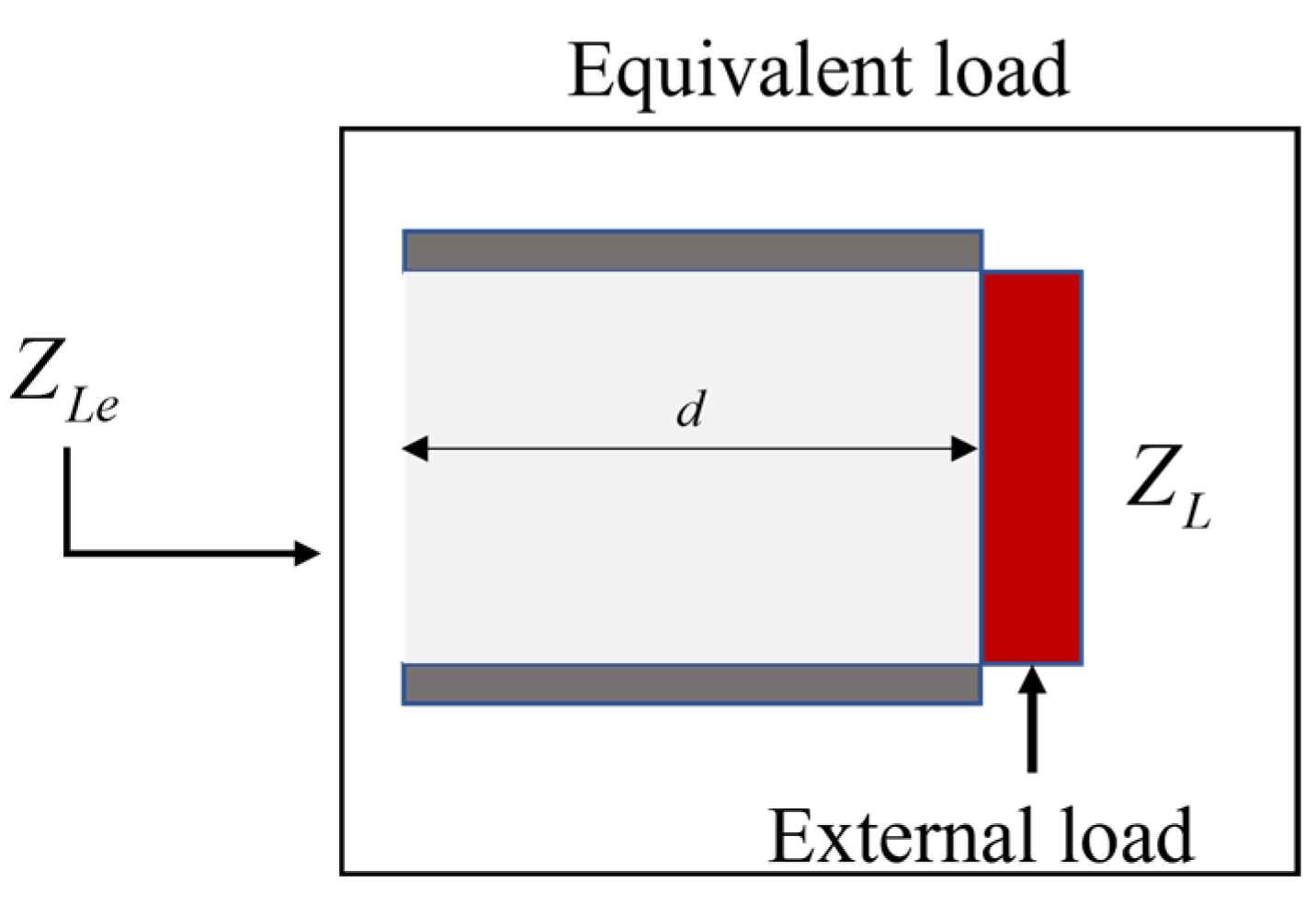
| Number | Measured Load Value ZL (Ω) | Measured Equivalent Load Value ZLe (Ω) |
|---|---|---|
| 1 | 101.3 − j56.8 | 126.2 + j165.3 |
| 2 | 189.6 − j136.0 | 158 + j48.7 |
| 3 | 507.0 + j40.5 | 346.6 − j150.3 |
| 4 | 302.1 − j228.4 | 165.7 − j49.4 |
| 5 | 196.2 − j76.6 | 199.7 + j8.5 |
| 6 | 119.9 − j28.1 | 166 + j186.2 |
| 7 | 229.2 − j129.6 | 185 + j30 |
| 8 | 187.6 + j29.8 | 297.3 + j178.7 |
| 9 | 158.7 − j364.3 | 69.4 − j58.5 |
| 10 | 190.5 − j382.8 | 78.1 − j71.4 |
| 11 | 222.7 + j30.5 | 325.2 + j133.2 |
| 12 | 198.6 − j89.5 | 192.3 + j74.0 |
| 13 | 127.0 − j58.7 | 152.6 + j148.2 |
| 14 | 171.4 − j193.6 | 120.6 + j21.5 |
| 15 | 568.8 − j547.7 | 122.5 − j185.7 |
| 16 | 199.3 − j247.1 | 116.3 − j16.9 |
| 17 | 207.0 − j90.0 | 197.4 + j67.9 |
| 18 | 143.7 − j48.5 | 176.3 + j146.9 |
Disclaimer/Publisher’s Note: The statements, opinions and data contained in all publications are solely those of the individual author(s) and contributor(s) and not of MDPI and/or the editor(s). MDPI and/or the editor(s) disclaim responsibility for any injury to people or property resulting from any ideas, methods, instructions or products referred to in the content. |
© 2024 by the authors. Licensee MDPI, Basel, Switzerland. This article is an open access article distributed under the terms and conditions of the Creative Commons Attribution (CC BY) license (https://creativecommons.org/licenses/by/4.0/).
Share and Cite
Liu, R.; Lai, S.; Hong, T.; Zhang, Z.; Dong, L.; Zhu, H.; Yang, Y. A Low-Reflection Tuning Strategy for Three-Stub Waveguides. Electronics 2024, 13, 1304. https://doi.org/10.3390/electronics13071304
Liu R, Lai S, Hong T, Zhang Z, Dong L, Zhu H, Yang Y. A Low-Reflection Tuning Strategy for Three-Stub Waveguides. Electronics. 2024; 13(7):1304. https://doi.org/10.3390/electronics13071304
Chicago/Turabian StyleLiu, Rufan, Shimiao Lai, Tao Hong, Zihao Zhang, Lu Dong, Huacheng Zhu, and Yang Yang. 2024. "A Low-Reflection Tuning Strategy for Three-Stub Waveguides" Electronics 13, no. 7: 1304. https://doi.org/10.3390/electronics13071304
APA StyleLiu, R., Lai, S., Hong, T., Zhang, Z., Dong, L., Zhu, H., & Yang, Y. (2024). A Low-Reflection Tuning Strategy for Three-Stub Waveguides. Electronics, 13(7), 1304. https://doi.org/10.3390/electronics13071304