Abstract
High-resolution electronics on complex curved surfaces have wide applications in fields such as biometric health monitoring, intelligent aircraft skins, conformal displays, and biomimetics. However, current manufacturing processes can only adapt to limited curvature, posing a significant challenge for achieving high-resolution fabrication of electronics on complex curved surfaces. In this study, we propose a novel fabrication strategy that combines electric field-driven jetting and water-assisted transfer printing techniques to achieve the fabrication of high-resolution electronics on complex curved surfaces. The electric field-driven jetting enables the fabrication of high-resolution 2D electronics on sacrificial layer substrates. After dissolving the sacrificial layer, it is observed that the 2D electronics form a self-supporting structure with a certain rigidity and flexibility. During the water-assisted transfer printing process, this self-supporting structure undergoes stretching deformation with excellent conformity of the electronics to curved surfaces while effectively minimizing wrinkles. Finally, we successfully demonstrate the manufacture of 25 μm high-resolution electronics on highly curved surfaces (nautilus shell) and complex (scallop shell, stone) surfaces. The integrity of transferred circuit patterns and consistency of conductors are verified through infrared thermography analysis, confirming the feasibility of this manufacturing strategy. In addition, a protective film with strong adhesive properties is sprayed onto the transferred curved circuits to enhance their adhesion and resistance to extreme environments such as acids and alkalis. Our proposed technique provides a simple and effective new strategy for the fabrication of high-resolution electronics on complex curved surfaces.
1. Introduction
High-resolution (~50 μm) electronics on complex curved surfaces is a type of electronics element with specific functionality in which the structure is prepared conformally to a complex curved surface. They have important application values in fields such as structural (e.g., fabrics, implantable chiplets) [1,2], wearable health-monitoring devices [3,4,5,6,7,8], intelligent aircraft skins [9] and smart robotics [10,11]. However, traditional manufacturing techniques like lithography [12,13,14], deposition [15,16], and micro-electro-mechanical system (MEMS) processes [17] face challenges in directly fabricating electronics structures on 3D complex surface substrates [18,19,20]. Hence, various manufacturing techniques have been explored to achieve the fabrication of high-resolution electronics on complex curved surfaces [21,22,23,24].
Fabrication techniques for high-resolution electronics on curved surfaces mainly include conformal printing [25,26,27] and transfer printing [28,29,30]. Conformal printing on curved surfaces involves techniques like electrohydrodynamic (EHD) jet printing [31,32,33], aerosol jet printing [34,35,36], inkjet printing [37,38,39,40], laser direct writing [41,42,43,44,45], and adaptive 3D printing [46]. For example, EHD jet printing on irregular or rough three-dimensional surfaces faces challenges due to the real-time variation of electric field strength, leading to unstable jets and difficult-to-achieve high-precision and stable printing on complex surfaces [47,48,49]. Aerosol jet printing is limited by material viscosity and poor wire edge roughness, resulting in poor electrical performance consistency [50]. Laser direct writing requires point-by-point scanning and involves cumbersome process steps [51]. Adaptive 3D printing can achieve high-quality printed results through automatic detection and height adjustment but requires expensive detection equipment and still struggles with achieving high-precision fabrication of arbitrarily complex curved surfaces [52]. In summary, surface conformal printing needs to be combined with five-axis machine tools, and high-precision printing relies on complex path planning, making it difficult to adapt to arbitrarily complex surface substrates [53].
The manufacturing process of conformal electronics based on transfer technology enables rapid fabrication of electronic structures on curved surfaces. Transfer processes mainly include stamp transfer, thermoforming transfer, thermal reflow-assisted transfer [54], and water transfer methods [55,56,57]. It is now possible to transfer high-precision patterns on smooth curved substrates; however, there are still issues such as distortion of electronic patterns during the transfer process and wrinkling when transferring from a two-dimensional plane to a non-developable curved surface [58]. It is also challenging to achieve high conformal adhesion on complex surface substrates. Therefore, developing a manufacturing method for high-resolution electronics suitable for complex curved surfaces is of great significance.
This study proposes a new method for manufacturing high-resolution electronics on complex curved surfaces by combining electric field-driven jetting [59,60] and water-assisted transfer printing. Firstly, high-resolution 2D electronics patterns are printed on a water-soluble cellulose sacrificial layer substrate using electric field-driven jetting. Subsequently, the 2D electronics pattern is placed in water, where we discovered that it forms a self-supporting structure during the sacrificial layer dissolution process. This self-supporting structure possesses a certain rigidity and flexibility, allowing for stretch deformation when transferred onto complex curved surfaces and achieving good conformity with complex curved surfaces. As a result, high-resolution electronics can be manufactured on complex surfaces. In addition, the tensile deformation produced by the self-supporting structure reduces wrinkles when transferring from a two-dimensional plane to a non-developable surface. We have succeeded in fabricating high-resolution electronics with line widths of about 25 μm on hemispherical transparent substrates as well as on various curved surfaces such as shells and stones. The hemispherical transparent 3D conformal electronics can function as transparent electric heaters with good light transmission, high heating performance, and heating stability. SEM images demonstrate excellent conformance of the high-resolution electronics on highly curved and complex surfaces, and the integrity of the circuit pattern after transfer and the consistency of the wires were also verified by infrared thermography.
2. Materials and Methods
2.1. Materials
Hydroxypropyl methyl cellulose (HPMC) was obtained from Shanghai Maclin Biochemical Technology Co., Ltd. (Shanghai, China). Nano-conductive silver paste with a high solid content (at 25 °C with a viscosity above 20,000 mPa·s, containing silver particles of 200–300 μm, silver content of 70–80%, and conductivity of 200 mΩ·μm) was obtained from Beijing Nano Top Electronic Technology Co., Ltd. (Beijing China). A water-based nano-coating emulsion (the water-based nano-coating was a milky emulsion with a solid content of 16–36% and a viscosity of 5000–9000 mPa·s at 23 °C) was obtained from Xianyou Ruilin Machinery Technology Co., Ltd. (Xianyou, China).
2.2. Methods
Step 1: Spin coating of sacrificial layer substrates. The substrate was subjected to a cleaning pretreatment by immersing float glass in alcohol for ultrasonic cleaning treatment for 3 min, followed by drying with nitrogen. Configuration of hydroxypropylmethylcellulose (HPMC) solution with a mass fraction of 5%: HPMC powder was added to DI water at 90 °C and stirred using a glass rod until the solution cooled. Finally, the solution was placed in a vacuum drying oven under vacuum to remove air bubbles from the solution. A homogeneous spin coating of the sacrificial layer film was performed using a Spin Coater at a speed of 1800 r/s for 40 s, followed by curing at an ambient temperature of 100 °C for 5 min. Step 2: Printing of high-resolution electronics on planar substrates by electric field-driven jetting. Optimum print parameter range: Air pressure ranges are 160–220 Pa, height ranges are 60–100 μm, speed range is 10–30 mm/s, and voltage range is 800–1000 V. Two-dimensional high-resolution planar electronics components were printed on sacrificial layer substrates using electric field-driven jetting and sintered at 100 °C for 40 min. Step 3: Transfer in water. The planar substrate was immersed in a water bath for 10 min. After the sacrificial layer fully dissolved, the 3D electronics were peeled off from the planar substrate using an auxiliary rod and placed on top of the curved substrate in water. The 3D conformal electronics were removed from the water once the 2D electronics were fully adhered to the curved substrate. Step 4: post-process. An aqueous nano-coating solution is sprayed on top of the complex curved surfaces with high-resolution electronics to create a closer bond between the electronics and the complex curved surfaces, which at the same time forms a protective layer for the electronics and enhances their electrical conductivity.
Step 1: Spin coating of sacrificial layer substrates. The substrate was subjected to a cleaning pretreatment by immersing float glass in alcohol for ultrasonic cleaning treatment for 3 min, followed by drying with nitrogen. Configuration of hydroxypropylmethylcellulose (HPMC) solution with a mass fraction of 5%: HPMC powder was added to DI water at 90 °C and stirred using a glass rod until the solution cooled. Finally, the solution was placed in a vacuum drying oven under vacuum to remove air bubbles from the solution. A homogeneous spin coating of the sacrificial layer film was performed using a Spin Coater at a speed of 1800 r/s for 40 s, followed by curing at an ambient temperature of 100 °C for 5 min. Step 2: Printing of high-resolution electronics on planar substrates by electric field-driven jetting. Optimum print parameter range: Air pressure ranges are 160–220 Pa, height ranges are 60 μm–100 μm, speed range is 10 mm/s–30 mm/s, and voltage range is 800 V–1000 V. Two-dimensional high-resolution planar electronics components were printed on sacrificial layer substrates using electric field-driven jetting and sintered at 100 °C for 40 min. Step 3: Transfer in water. The planar substrate was immersed in a water bath for 10 min. After the sacrificial layer fully dissolved, the 3D electronics were peeled off from the planar substrate using an auxiliary rod and placed on top of the curved substrate in water. The 3D conformal electronics were removed from the water once the 2D electronics were fully adhered to the curved substrate. Step 4: post-process. An aqueous nano-coating solution is sprayed on top of the complex curved surfaces with high-resolution electronics to create a closer bond between the electronics and the complex curved surfaces, which at the same time forms a protective layer for the electronics and enhances their electrical conductivity.
2.3. Characterisation
High-resolution electronics on a complex curved surface was characterized using scanning electron microscopy (MERLIN Compact, Zeiss, Oberkochen, Germany) and optical microscopy (DXS510, OLYMPUS, Tokyo, Japan). Characterization of circuit resistance was performed using AT516 from China Applied Instruments Co., Ltd. (Shanghai, China) and infrared thermal imaging was carried out with C5 from FLIR (Wilsonville, OR, USA). Characterization of visible light transmittance was performed using the Shanghai Yuanyi Instrument Co., Ltd. UV-100 (Changzhou, China).
3. Results and Discussion
3.1. Exploration of Fabrication Process and Technological Parameter Laws for 3D Surface Conformal Circuits
This study introduces a novel method for manufacturing high-resolution electronics on complex curved surfaces by integrating electric field-driven jetting and water-assisted transfer printing. The technical principle and process are illustrated in Figure 1a–f. The reason why we chose HPMC as the sacrificial layer material is that HPMC has good water solubility. At the same time, during the dissolution process, the HPMC film will not swell and will not damage the circuit on the surface of the sacrificial layer film. The sacrificial layer film was coated using the spin coater. After completing the spin-coating of the sacrificial layer film, the printing of high-resolution electronics on planar substrates by electric field-driven jetting is shown in Figure 1b,c. The printhead is connected to the positive pole of the power supply, causing the conductive silver paste at the nozzle to form a polarized charge. The print nozzle, under the action of the DC voltage, interacts with the high-potential substrate to induce electrostatic effects. This results in the formation of a very fine Taylor cone jet, enabling high-resolution printing. Figure 1d–f illustrate the process of water-assisted transfer printing. The grid structure, different from the line grid, provides support from two directions to form a self-supporting structure. Also, printing via electric field-driven jetting technology ensures that the circuits are homogeneous, which results in roughly equal gravity among the parts of the circuits. The 2D electronics can maintain their original shape in water without deformation. After detachment from the planar base, the 2D electronics can be transferred to the complex curved surface. At this point, due to the different order of contact among the electronics and the curved substrate, the untouched portion has a greater gravity force relative to the contacted portion. At this point, a certain amount of pulling occurs, and the electronics deform under this phenomenon. After stretching, the co-conformity between the electronics and the curved substrate is optimized. When the complex curved surface base with high-resolution electronics is lifted out of the water, the pressure formed by the surface tension of the liquid drives the microcircuits to unfold along the surface, ensuring conformality among the electronics and the complex curved surface. Figure 1g–l display the microscopic images of the 2D electronics and 3D conformal electronics. After transferring from the planar to the complex curved surface (stone), the form of the electronics stays the same, confirming the grid structure’s excellent self-supporting capability. The integrity of the electronics structure is maintained before and after the transfer, ensuring the performance of the circuit remains unchanged.
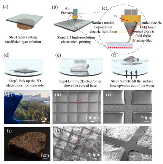
Figure 1.
Schematic of the process flow for the preparation of high-resolution electronics on complex curved surfaces by combining electric field-driven jetting and water-assisted transfer printing techniques: (a) Spin-coating the sacrificial layer; (b) Printing the 2D electronics on the planar surface; (c) Electric field-driven jetting principle; (d) 2D electronics falling off; (e) Moving the 2D electronics above the complex curved surfaces; (f) Holding out the curved surface from the water; (g) Macro image of a 2D electronics; (h,i) SEM images of (g) local enlargements; (j) Macro image of the high-resolution electronics on the complex curved surfaces; (k,l) SEM images of (j) and local enlargements.
Two-dimensional planar circuits have a direct impact on the resolution and consistency of curved circuits, which may have an impact on the performance of the electronics. The goal of this study is to achieve the fabrication of high-precision electronic devices below 50 μm. So, it is necessary to investigate the effect of electric field-driven jetting process parameters (voltage, air pressure, print height, speed) on the width and shape of 2D planar circuit lines. As depicted in Figure 2a–d, we investigated the 2D high-resolution electronic printing parameters. For this study, a glass nozzle with an inner diameter of 40 μm was chosen. The standard parameters were set at a printing voltage of 800 V, a printing speed of 20 mm/s, a printing height of 80 μm, and an air pressure of 220 Pa. By altering each parameter, the impact on the printing effect was investigated. Air pressure has a significant impact on the printing process per unit of time at the nozzle. Lower air pressure leads to insufficient material supply, whereas excessive air pressure causes paste build-up in the nozzle. The air pressure range is typically set between 140 Pa and 300 Pa, with a test interval of 20 Pa. The print pattern is illustrated in Figure 2a. As the air pressure increases, the print line width also increases. At 140 Pa, the print line width is 12.58 μm, which rises to 31.1 μm when the air pressure reaches 300 Pa. In the end, we optimized the air pressure range from 160 Pa to 220 Pa. The printing height directly affects the stability of the electric field force. When the distance between the nozzle and substrate is reduced, although reducing the nozzle and substrate distance increases the electric field force and enhances the electric field on the conductive paste pull, resulting in a more stable circuit, it also causes a decrease in print resolution. Conversely, increasing the distance reduces the electric field effect, leading to instability of the Taylor cone and inconsistent print morphology, resulting in an unstable resistance of the electronics and an increased edge roughness. Figure 2b displays the test executed within the print height range of 30 μm–120 μm at an interval of 10 μm. Elevating printing height leads to a decline in line width from 21.3 μm to 17.4 μm, but contrarily, it diminishes line width consistency. Increasing the printing speed of circuits has a positive impact on reducing line width by enhancing the drag pull of Taylor cones. Therefore, our preferred print height ranges from 60 μm to 100 μm. However, if the printing speed and paste supply speed are mismatched, this can cause necking or even lead to broken points. To investigate this phenomenon, we conducted circuit testing at print speeds ranging from 3 mm/s to 70 mm/s, as shown in Figure 2c. Nevertheless, it resulted in the instability of the morphology. As the printing speed increased, the line width decreased from 48.68 μm to 9.662 μm. Nevertheless, it also resulted in the instability of the morphology. Therefore, our preferred printing speed range is 10 mm/s–30 mm/s. Finally, the impact of printing voltage on printing quality is evaluated. When the applied voltage is low, the electric field force induced is also low, causing an unstable Taylor cone, which ultimately leads to a suboptimal pulling effect on the printing paste. Consequently, the printed electronics line width presents discontinuities or poor consistency. Conversely, overlarge voltages produce excessive electric field force, disrupting the equilibrium of the Taylor cone. To restore the balance, the printing paste offsets it by increasing its surface tension. Excessive electric field force and increased surface tension during printing can cause the circuit board to curve, develop burrs, and result in satellite droplets, among other phenomena. To maintain consistent printing conditions, the amount of paste extruded from the nozzle per unit of time must remain constant. However, the curvature caused by the electric field force at the nozzle results in the paste being extruded over a longer distance, ultimately leading to thinner circuit line widths. As demonstrated in Figure 2d, at a voltage of 2000 V, there is the presence of non-continuous droplets on the shape. At 2000 V, since the circuit has now become an irregular shape, its line width is immeasurable. So, finally, our preferred voltage range is 800 V–1000 V. This section explores the effects of printing voltage, printing pressure, printing height, printing speed, and other parameters on the line width and line appearance of the 2D high-resolution electronics through systematic experiments, and selects the optimal range of process parameters to provide experimental guidance for the manufacture of high-precision 2D planar electronics; this is an important basis for the fabrication of high-resolution electronics on complex curved surfaces.
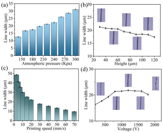
Figure 2.
Two-dimensional electronics printing parameter laws: (a) Print air pressure and electronics resolution relationship; (b) Print height and electronics resolution relationship and microstructure; (c) Print speed and electronics resolution relationship; (d) Print voltage and electronics resolution relationship and microstructure.
3.2. High-Resolution Electronics Manufacturing for Developable and Non-Developable Complex Surfaces
Surface substrates can be classified into two groups. The first group comprises extensible surfaces, which are completely conformable to a planar structure without stretching or compressing, as long as there are no creases. The second group comprises non-developable surfaces, which can only be deformed by matching the curvature of each point on the surface. The curvature cannot be changed unless the surface is stretched or compressed, as it is inherent to the surface. As a result, mathematical language is utilized to analyze the surface [61,62,63].
where K is the Gaussian curvature and k1 and k2 are the curvatures in the two directions.
K = k1 × k2
For a plane, it has zero curvature in both directions, i.e., k1 = 0 and k2 = 0, so:
K = 0 × 0 = 0
For extensible surfaces (e.g., cylinders, cones), which have zero curvature in one direction, i.e., k1 = 0, and non-zero curvature in the other direction, i.e., k2 = k2, then:
K = 0 × k2 = 0
In either circumstance, the Gaussian curvature is zero, indicating that they share the same curvature. Consequently, the surface can be changed into a flat structure, and similarly, the flat structure can be changed into the corresponding surface arrangement.
Of course, there is another case, for non-developable surfaces: k1 and k2 are not zero. At this time:
K = k1 × k2 ≠ 0
In this case, the identical curvature as described previously is unavailable, rendering surface-to-plane transformations unfeasible.
The following is a structural characterization of the electronics transfer effect of some representative non-developable epitaxial substrate structures, whose macroscopic and scanning electron microscope (SEM) microscopic magnifications are shown in Figure 3a–o. The 3D conformal electronics circuit lines have a width of about 25 μm, and the periods of the circuits are all 500 μm. As shown in Figure 3a–c, the transfer onto the surface of the shell demonstrates that our technique can be adapted for complex surfaces to a great extent, and even on complex curved surfaces it still shows good conformal ability. Figure 3d–f exhibit the conformability of microcircuits with non-developable, smooth surfaces. Due to the self-support ability of the grid structure, it still maintains its original shape after transfer. Meanwhile, mesh-structured electronic structures can deform slightly due to bi-directional support, allowing them to be more adaptable to substrates when conformable to said surface. Figure 3i,j depict the flexibility of the circuits when applied to uneven substrates and their potential to flawlessly adhere to intricate surfaces and sustain their structure. As shown in Figure 4a–h, we prepared high-resolution electronics with a line width of 25 μm on glass, scallop shells, conch shells, and stone surfaces and tested the 3D surface conformal circuits by thermography with a 2V DC voltage. As shown in Figure 4a,c,e,g, we can observe from the macroscopic images that the high-resolution electronics still maintain a stable mesh structure after transferring to the curved surface substrate, and at the same time, the wrinkles caused by 2D to 3D mismatches are not obvious due to the stretching nature of self-supporting meshes. As shown in Figure 4b,d,f,h, the heating performance of high-resolution electronics fabricated using the same structural parameters is compared on different types of substrates. The thermal imaging shows that the high-resolution electrons display uniform heating on planar substrates (glass plates), large-curvature substrates (conch shells), and arbitrarily complex curved substrates (including scallop shells and stones), without any obvious hot spots or dark spots. This phenomenon of uniform heating suggests that the electronics retain their original mesh structure both before and after the transfer process and exhibit excellent conformal properties on complex surfaces. At the same time, the electronics are not broken, and their electrical properties remain consistent before and after the transfer, which also confirms that the planar electronics fabricated by electric field-driven jetting have good mechanical strength. The self-supporting mesh structure and water-assisted transfer technology also ensure that the electronics are subjected to less stress during the transfer process and keep the pattern free of distortion. These findings indicate that our technique is well suited for applications to surfaces with large curvature and arbitrary complexity.
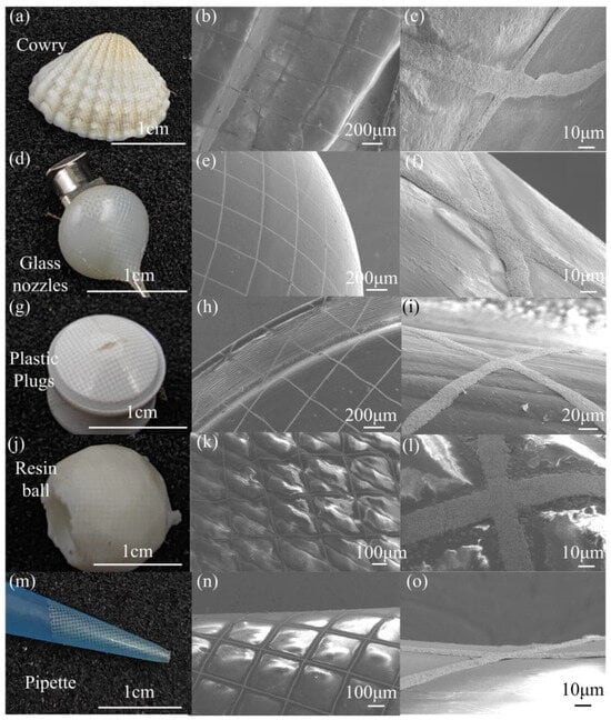
Figure 3.
Macro- and microstructures of high-resolution electronics on typical complex curved surfaces: (a–c) Macro- and microstructures of high-resolution electronics on shell substrate; (d–f) Macro- and microstructures of high-resolution electronics on hot-melt adhesive substrates; (g–i) Macro- and microstructures of high-resolution electronics on plastic plug base; (j–l) Macro- and microstructures of high-resolution electronics on resin sphere substrate; (m–o) Macro- and microstructures of high-resolution electronics on pipette bases.
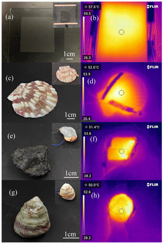
Figure 4.
Macroscopic imaging and thermal imaging testing of high-resolution electronics on large-curvature and arbitrarily complex surface substrates: (a) Macroscopic image of high-resolution electronics on glass pane substrate; (b) Thermal imaging testing of the high-resolution electronics on glass pane substrate; (c) Macroscopic image of high-resolution electronics on scallop shell substrate; (d) Thermal imaging testing of the high-resolution electronics on scallop shell substrate; (e) Macroscopic image of high-resolution electronics on stone substrate; (f) Thermal imaging testing of high-resolution electronics on scallop substrate; (g) Macroscopic image of high-resolution electronics on conch shell substrate; (h) Thermal imaging tests of high-resolution electronics on conch shell substrates.
3.3. Investigation of the Application in Curved Transparent Electric Heaters
The curved transparent heater is an electronic element with excellent optoelectronic properties, while at the same time, it can be Joule-heated by its good electrical conductivity. It has a wide range of applications in outdoor surveillance cameras, weapon observation systems, and other fields. In the current technological context, curved transparent electric heaters with excellent optoelectronic properties are difficult to fabricate simply and efficiently. We fabricated a curved transparent electric heater on an acrylic dome substrate and tested it for performance indicators.
Transmittance is one of the most important indicators of curved transparent electric heaters, and we tested the optical transmittance before and after the transfer. Figure 5a,b show the optical transmittance performance tests before and after the transfer of 2D electronics from planar to curved surfaces for circuits with a period of 200–1000 μm. Before transfer, high-resolution electronics with a period of 200 μm, 250 μm, 300 μm, 500 μm, 750 μm and 1000 μm can achieve 83.59%, 87.24%, 90.18%, 91.76%, 92.69% and 97.11% (at 550 nm) transmittance, respectively, after subtracting the effect of the substrate. The transfer of two-dimensional planar electronics onto a non-developable curved substrate can result in incompatibility between the planar pattern and the non-developable substrate, which can cause the planar pattern to bend and fold out of shape, affecting the transmittance of the conformal electrons. Because we prepare high-resolution electronics with microscale line width and microstretching properties from self-supporting grids, although the appearance of creases can be reduced, the effect of wrinkles on light transmittance is greatly reduced. Despite the degradation of optical performance caused by the transfer of the printed circuit, high-resolution electronics with periods of 200 μm, 250 μm, 300 μm, 500 μm, 750 μm, and 1000 μm still achieve transmittance values of 68.75%, 73.05%, 77.37%, 86.12%, 89.53%, and 91.7% (at a wavelength of 550 nm), respectively, after accounting for the substrate. It shows that there is not too much wrinkling before and after the transfer, which also reflects that a good conformal effect can be achieved between the self-supporting mesh and the curved surface.
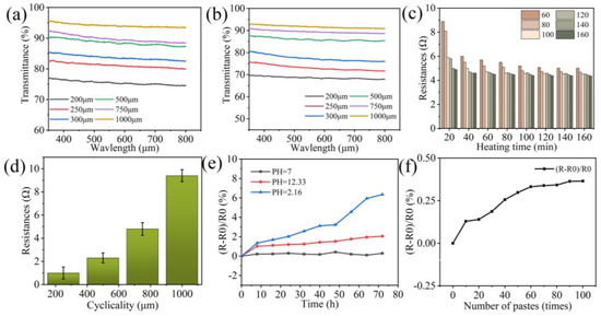
Figure 5.
Characterization of the properties of acrylic dome conformal circuits; (a) Transmittance of circuits before transfer; (b) Transmittance of circuits after transfer; (c) Resistance relations for circuits with different cycles; (d) Effect of heating temperature and heating time on circuit resistance; (e) Chemical stability test; (f) Adhesion test.
Conductivity determines the heating ability of curved transparent electric heaters, so we tested the electrical performance and stability of curved transparent electric heaters. Investigating the effect of sintering parameters on electrical conductivity was carried out in the range of 80 °C–160 °C with an interval of 20 °C. As shown in Figure 5c, between 0–20 min, the resistance value decreased significantly. This is due to the rapid volatilization of the organic solvent in the conductive paste at this stage, and the nanosilver particles in the paste came in close contact. After 40 min, the volatilization of the organic solvent was almost finished, and the resistance of the paste was stabilized. Overall, the conductivity improves with increasing sintering time and temperature, but since the acrylic substrate cannot withstand high temperatures above 100 °C, in this study we chose to carry out curing at an ambient temperature of 100 °C for 40 min. As shown in Figure 5d, we tested the resistance value of the electronics after curing with different cycles, and the resistance value is only 1.02 Ω at a cycle of 250 μm and 2.3 Ω at 500 μm. After weighing the conductivity and light transmission, we chose 500 μm as the electronics circuit cycle of the curved transparent electric heater. However, curved transparent electric heaters will inevitably encounter harsh working environments in practical applications, so to test the adaptability of curved transparent electric heaters to the environment, we coated a nano-coating on the surface of the curved transparent electric heater as a protective layer and carried out chemical stability and adhesion tests. The resistors were immersed in dilute hydrochloric acid solution at PH = 2.16, sodium hydroxide solution at PH = 12.33, and DI water at PH ≈ 7 for 72 h. The resistance change rate, as shown in Figure 5e, was only 6.35% at PH = 2.16 after 72 h of testing and 2.05% in the alkaline solution; there was almost no change in neutral solution, which also demonstrates the good chemical stability of our fabricated 3D surface conformal circuit. For the stability of the adhesion force in use, we conducted 100 adhesion-force tests; as shown in Figure 5f, the resistance change of the nano-coated conformal circuits is only 0.36%, which is almost negligible after 100 adhesion tests using the 3M tape.
As shown in Figure 6a–c, we prepared high-resolution electronics with an area of 60 × 60 mm and a cycle of 500 μm on an acrylic hemispherical cover with a line width of only 25 μm, which is almost invisible to the naked eye under natural light, and conducted heating tests on the heater with voltages of 2 V, 2.5 V, 3 V, 3.5 V, and 4 V, as shown in Figure 6d–h, where maximum temperatures of 56.7 °C, 70.3 °C, 83.9 °C, 97.5 °C and 118 °C can be reached, the heating temperature can approach the boiling point of water at 3.5 V and exceed it at 4 V, which reveals a better heating effect. Thermal imaging images also show that the curved transparent heater has a uniform heating effect, which also indicates that the high-resolution electronics still have a good conformal fit on the smooth non-developable curved substrate. As shown in Figure 6i, the thermal response test shows that the maximum temperature can be reached within 300 s at all voltages from 2 V to 3.5 V; at 4 V, the temperature can reach 109 °C within 300 s and the maximum temperature of 118 °C at 500 s, which then slowly falls to room temperature. To test the heat stability of the curved conformal circuit, we performed 100 thermal cycle tests at 4 V, heated the heater to the maximum temperature and turned off the power, and waited for the circuit to ride to room temperature for the next test. The test results are shown in Figure 6j. Under 100 thermal cycles, the maximum temperature reached by the heater as well as the heating time required to heat up to the maximum temperature is the same, and there is no obvious difference between the first 10 times and the last 10 times, which also proves that the curved transparent heater prepared in this work has good heating stability.
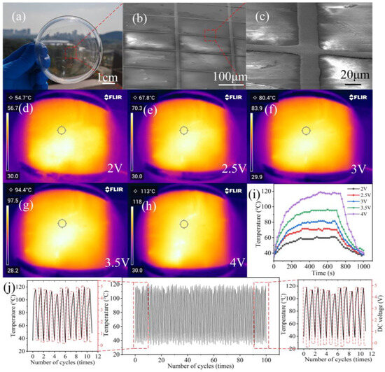
Figure 6.
Characterization of micro-morphology and performance of curved transparent electric heaters: (a) Macro image of a conformal circuit with acrylic dome cover; (b,c) SEM images of (a) as well as local enlargements; (d–h) Maximum temperatures corresponding to curved transparent heater with different voltages; (i) Temperature rise curve of curved transparent heater with different voltages; (j) Curved transparent electric heater 100 times thermal cycle curve.
4. Conclusions
In summary, we propose a new method combining electric field-driven jetting and water-assisted transfer for fabricating high-resolution electronics on complex surfaces, which allows simple and efficient fabrication of high-resolution electronics on complex surfaces. Firstly, high-resolution planar electronic circuits are printed using electric field-driven jetting. During the water-assisted transfer printing process, the self-supporting structure formed by the electronic circuits can undergo stretching deformation, reducing wrinkling and ensuring a good fit onto complex surface substrates. We successfully fabricated high-resolution electronics with a line width of 25 μm on large-curvature (conch shells) and arbitrarily complex curved surfaces (scallop shells, stones) as substrates. Thermal imaging tests demonstrate that the integrity of the electronic circuit structures is maintained before and after transfer, with good consistency across circuits. Finally, the application of curved surface electronic circuits in the field of curved transparent electric heating was explored. The acrylic hemispherical curved transparent heater manufactured achieved a high transmittance rate of 91.8% and exhibited excellent environmental and mechanical stability. It could reach a heating temperature of 118 °C at 4 V. With the increasing demand for high-resolution electronics on complex curved surfaces, existing manufacturing methods make it difficult to achieve conformal fabrication of high-resolution electronic circuits. Our proposed fabrication method undoubtedly provides an effective and feasible new solution for the fabrication of high-resolution electronics on complex curved surfaces. However, this transfer printing method also has limitations, such as difficulties in eliminating wrinkles and being unsuitable for large areas. Currently, we have successfully reduced the occurrence of wrinkles through experimental methods, such as utilizing the stretching deformation of self-supporting structures to conform better to complex surfaces. In the future, we will optimize the design of electronic structures through theoretical modeling, simulation and other methods to enable higher precision conformal electronics manufacturing of complex surfaces.
Author Contributions
Conceptualization, Z.L. and X.Z.; methodology W.S. and H.Z.; software, W.S., Z.L. and H.Z.; validation, X.Z., W.S. and H.L. (Hongke Li); formal analysis, W.S., H.L. (Hongke Li) and R.W.; investigation, Z.L. and G.Z.; resources, X.Z. and H.L. (Hongbo Lan); data curation, W.G. and F.W.; writing—original draft preparation, W.S.; writing—review and editing, X.Z., Z.L., C.L. and F.Z.; supervision, H.C.; project administration, X.D. All authors have read and agreed to the published version of the manuscript.
Funding
This study was supported by the National Natural Science Foundation of China (Grant No. 52375348, 52175331) and the National Natural Science Foundation of Shandong Province (Grant No. ZR2022ME014, ZR2020ZD04).
Data Availability Statement
The data presented in this study are available in this article.
Conflicts of Interest
The authors declare no conflicts of interest. Author Chaohong Liu was employed by the company Goertek Inc. The author declares that the research was conducted in the absence of any commercial or financial relationships that could be construed as a potential conflict of interest.
References
- Shahariar, H.; Jur, J.S. Correlation of printing faults with the RF characteristics of coplanar waveguides (CPWs) printed on nonwoven textiles, Sens. Actuator A Phys. 2018, 273, 240–248. [Google Scholar] [CrossRef]
- Jeong, J.; Laiwalla, F.; Lee, J.; Ritasalo, R.; Pudas, M.; Larson, L.; Leung, V.; Nurmikko, A. Conformal Hermetic Sealing of Wireless Microelectronic Implantable Chiplets by Multilayered Atomic Layer Deposition (ALD). Adv. Funct. Mater. 2019, 5, 1806440. [Google Scholar] [CrossRef]
- Zhao, X.L.; Tong, Y.H.; Tang, Q.X.; Liu, Y.C. Wafer-Scale Coplanar Electrodes for 3D Conformal Organic Single-Crystal Circuits. Adv. Electron. Mater. 2015, 12, 10. [Google Scholar] [CrossRef]
- Wang, R.; Zhu, X.Y.; Sun, L.F.; Shang, S.; Li, H.K.; Ge, W.S.; Lan, H.B. Cost-Effective Fabrication of Transparent Strain Sensors via Micro-Scale 3D Printing and Imprinting. Nanomaterials 2022, 12, 120. [Google Scholar] [CrossRef]
- Guan, S.J.; Yang, Y.; Wang, Y.Y.; Zhu, X.; Ye, D.D.; Chen, R.; Liao, Q. A Dual-Functional MXene-Based Bioanode for Wearable Self-Charging Biosupercapacitors. Adv. Mater. 2023, 36, 10. [Google Scholar] [CrossRef]
- Takei, K.; Honda, W.; Harada, S.; Arie, T.; Akita, S. Toward Flexible and Wearable Human-Interactive Health-Monitoring Devices. Adv. Healthc. Mater. 2015, 4, 4. [Google Scholar] [CrossRef]
- Hu, X.Y.; Dou, Y.Y.; Li, J.J.; Liu, Z.F. Buckled Structures: Fabrication and Applications in Wearable Electronics. Small 2019, 15, 26. [Google Scholar] [CrossRef]
- Chow, P.C.Y.; Someya, T. Organic Photodetectors for Next-Generation Wearable Electronics. Adv. Mater. 2020, 32, 26. [Google Scholar] [CrossRef]
- Zhou, J.Z.; Li, H.T.; Kang, L.; Tang, B.F.; Huang, J.; Cai, Z.H. Design, Fabrication, and Testing of Active Skin Antenna with 3D Printing Array Framework. Int. J. Antennas Propag. 2017, 2017, 7516323. [Google Scholar] [CrossRef]
- Huang, Y.A.; Wu, H.; Zhu, C.; Xiong, W.N.; Chen, F.R.; Xiao, L.; Liu, J.P.; Wang, K.X.; Li, H.Y.; Ye, D.; et al. Programmable robotized ‘transfer-and-jet’ printing for large, 3D curved electronics on complex surfaces. Int. J. Extreme Manuf. 2021, 4, 14. [Google Scholar] [CrossRef]
- Shintake, J.; Cacucciolo, V.; Floreano, D.; Shea, H. Soft Robotic Grippers. Adv. Mater. 2018, 30, 33. [Google Scholar] [CrossRef]
- Zou, Y.; Moreel, L.; Lin, H.T.; Zhou, J.; Li, L.; Danto, S.; Musgraves, J.D.; Koontz, E.; Richardson, K.; Dobson, K.D.; et al. Solution Processing and Resist-Free Nanoimprint Fabrication of Thin Film Chalcogenide Glass Devices: Inorganic-Organic Hybrid Photonic Integration. Adv. Opt. Mater. 2014, 8, 759–764. [Google Scholar] [CrossRef]
- Yang, P.; Ju, Y.K.; Hu, Y.; Xie, X.Y.; Fang, B.R.; Lei, L.J. Emerging 3D bioprinting applications in plastic surgery. Biomater. Res. 2023, 1, 27. [Google Scholar] [CrossRef]
- Zhang, M.; Liu, X.; Cao, A.X.; Pang, H.; Shi, L.F.; Deng, Q.L. Polymer Periodic Nanostructures on Curved Substrates by UV-Curable Hybrid Soft Nanoimprint Lithography. Nanosci. Nanotechnol. Lett. 2017, 12, 2101–2104. [Google Scholar] [CrossRef]
- Goh, G.L.; Dikshit, V.; Koneru, R.; Peh, Z.K.; Lu, W.Y.; Goh, G.D.; Yeong, W.Y. Fabrication of design-optimized multifunctional safety cage with conformal circuits for drone using hybrid 3D printing technology. Int. J. Adv. Manuf. Technol. 2022, 3–4, 2573–2586. [Google Scholar] [CrossRef]
- Cheng, L.X.; Adinolfi, V.; Weeks, S.L.; Barabash, S.V.; Littau, K.A. Conformal deposition of GeTe films with tunable Te composition by atomic layer deposition. J. Vac. Sci. Technol. 2019, 2, 7. [Google Scholar] [CrossRef]
- Chen, X.Y.; Chen, Z.M.; Xiao, L.; Hao, Y.G.; Wang, H.; Ding, Y.T.; Zhang, Z.Y. Fabrication and Electrical Characterization of High Aspect Ratio Through-Silicon Vias with Polyimide Liner for 3D Integration. Micromachines 2022, 7, 1147. [Google Scholar] [CrossRef]
- Sloma, M. 3D printed electronics with nanomaterials. Nanoscale 2023, 12, 5623–5648. [Google Scholar] [CrossRef]
- Zhu, H.; Yao, C.; Wei, B.Y.; Xu, C.Y.; Huang, X.X.; Liu, Y.; He, J.K.; Zhang, J.N.; Li, D.C. 3D printing of functional bioengineered constructs for neural regeneration: A review. Int. J. Extreme Manuf. 2023, 4, 32. [Google Scholar] [CrossRef]
- Wang, Z.; Zhang, B.; He, Q.; Chen, H.; Wang, J.; Yao, Y.; Zhou, N.; Cui, W. Multimaterial Embedded 3D Printing of Composite Reinforced Soft Actuators. Research 2023, 6, 11. [Google Scholar] [CrossRef]
- Li, W.W.; Liu, J.; Wei, J.N.; Yang, Z.Y.; Ren, C.L.; Li, B.X. Recent Progress of Conductive Hydrogel Fibers for Flexible Electronics: Fabrications, Applications, and Perspectives. Adv. Funct. Mater. 2023, 17, 28. [Google Scholar] [CrossRef]
- Zhang, D.S.; Liu, R.J.; Li, Z.G. Irregular LIPSS produced on metals by single linearly polarized femtosecond laser. Int. J. Extreme Manuf. 2022, 1, 11. [Google Scholar] [CrossRef]
- Zhang, H.C.; Zhu, X.Y.; Tai, Y.P.; Zhou, J.Y.; Li, H.K.; Li, Z.H.; Wang, R.; Zhang, J.B.; Zhang, Y.C.; Ge, W.S.; et al. Recent advances in nanofiber-based flexible transparent electrodes. Int. J. Extreme Manuf. 2023, 3, 55. [Google Scholar] [CrossRef]
- Wang, L.; Fu, X.M.; He, J.Q.; Shi, X.; Chen, T.Q.; Chen, P.N.; Wang, B.J.; Peng, H.S. Application Challenges in Fiber and Textile Electronics. Adv. Mater. 2020, 5, 25. [Google Scholar] [CrossRef]
- Armstrong, C.D.; Montgomery, S.M.; Yue, L.; Demoly, F.; Zhou, K.; Qi, H.J. Robotic Conformal Material Extrusion 3D Printing for Appending Structures on Unstructured Surfaces. Early Access 2024, 9, 2300516. [Google Scholar] [CrossRef]
- Ng, L.W.T.; Zhu, X.X.; Hu, G.H.; Macadam, N.; Um, D.; Wu, T.C.; Le Moal, F.; Jones, C.; Hasan, T. Conformal Printing of Graphene for Single- and Multilayered Devices onto Arbitrarily Shaped 3D Surfaces. Adv. Funct. Mater. 2019, 29, 12. [Google Scholar] [CrossRef]
- Han, L.; Lin, J.; Liu, J.; Fahrenkrug, E.; Guan, Y.L.; Sun, K.; Wang, Y.Q.; Liu, K.; Wang, Z.J.; Wang, Z.G.; et al. Spatioselective Growth on Homogenous Semiconductor Substrates by Surface State Modulation. Nano Lett. 2021, 21, 14. [Google Scholar] [CrossRef]
- Zhang, S.; Luo, H.Y.; Wang, S.H.; Chen, Z.; Nie, S.; Liu, C.Y.; Song, J.Z. A thermal actuated switchable dry adhesive with high reversibility for transfer printing. Int. J. Extreme Manuf. 2021, 3, 9. [Google Scholar] [CrossRef]
- Xiong, S.X.; Li, J.; Peng, J.L.; Dong, X.Y.; Qin, F.; Wang, W.; Sun, L.L.; Xu, Y.L.; Lin, Q.Q.; Zhou, Y.H. Water Transfer Printing of Multilayered Near-Infrared Organic Photodetectors. Adv. Opt. Mater. 2022, 10, 7. [Google Scholar] [CrossRef]
- Serra, P.; Piqué, A. Laser-Induced Forward Transfer: Fundamentals and Applications. Adv. Mater. Technol. 2019, 1, 33. [Google Scholar] [CrossRef]
- Lee, J.S.; Kim, S.Y.; Kim, Y.J.; Park, J.; Kim, Y.; Hwang, J.; Kim, Y.J. Design and evaluation of a silicon based multi-nozzle for addressable jetting using a controlled flow rate in electrohydrodynamic jet printing. Appl. Phys. Lett. 2008, 93, 3. [Google Scholar] [CrossRef]
- Bi, S.; Wang, R.Y.; Han, X.; Wang, Y.; Tan, D.C.; Shi, B.O.; Jiang, C.M.; He, Z.R.; Asare-Yeboah, K. Recent Progress in Electrohydrodynamic Jet Printing for Printed Electronics: From 0D to 3D Materials. Coatings 2023, 7, 1150. [Google Scholar] [CrossRef]
- Morad, M.R.; Rajabi, A.; Razavi, M.; Sereshkeh, S.R.P. A Very Stable High Throughput Taylor Cone-jet in Electrohydrodynamics. Sci. Rep. 2016, 6, 10. [Google Scholar] [CrossRef]
- Fisher, C.; Skolrood, L.N.; Li, K.; Joshi, P.C.; Aytug, T. Aerosol-Jet Printed Sensors for Environmental, Safety, and Health Monitoring: A Review. Adv. Mater. Technol. 2023, 15, 37. [Google Scholar] [CrossRef]
- Zhang, H.N.; Moon, S.K. Reviews on Machine Learning Approaches for Process Optimization in Noncontact Direct Ink Writing. ACS Appl. Mater. Interfaces 2021, 45, 45. [Google Scholar] [CrossRef]
- Vella, S.; Smithson, C.; Halfyard, K.; Shen, E.; Chrétien, M. Integrated capacitive sensor devices aerosol jet printed on 3D objects. Flex. Print. Electron. 2019, 4, 16. [Google Scholar] [CrossRef]
- Ge, Q.; Li, Z.Q.; Wang, Z.L.; Kowsari, K.; Zhang, W.; He, X.N.; Zhou, J.L.; Fang, N.X. Projection micro stereolithography based 3D printing and its applications. Int. J. Extreme Manuf. 2020, 2, 19. [Google Scholar] [CrossRef]
- Park, Y.G.; Yun, I.; Chung, W.G.; Park, W.; Lee, D.H.; Park, J.U. High-Resolution 3D Printing for Electronics. Adv. Sci. 2022, 8, 29. [Google Scholar] [CrossRef] [PubMed]
- Goh, G.L.; Zhang, H.N.; Chong, T.H.; Yeong, W.Y. 3D Printing of Multilayered and Multimaterial Electronics: A Review. Adv. Electron. Mater. 2021, 10, 28. [Google Scholar] [CrossRef]
- Zhu, X.Y.; Liu, M.Y.; Qi, X.M.; Li, H.K.; Zhang, Y.F.; Li, Z.H.; Peng, Z.L.; Yang, J.J.; Qian, L.; Xu, Q.; et al. Templateless, Plating-Free Fabrication of Flexible Transparent Electrodes with Embedded Silver Mesh by Electric-Field-Driven Microscale 3D Printing and Hybrid Hot Embossing. Adv. Mater. 2021, 33, 2007772. [Google Scholar] [CrossRef] [PubMed]
- Yi, N.; Gao, Y.Y.; Verso, A.L.; Zhu, J.; Erdely, D.; Xue, C.L.; Lavelle, R.; Cheng, H.Y. Fabricating functional circuits on 3D freeform surfaces via intense pulsed light-induced zinc mass transfer. Mater. Today 2021, 50, 24–34. [Google Scholar] [CrossRef]
- Li, Y.; Wei, Y.; Yang, Y.B.; Zheng, L.; Luo, L.; Gao, J.W.; Jiang, H.J.; Song, J.C.; Xu, M.Z.; Wang, X.W.; et al. The Soft-Strain Effect Enabled High-Performance Flexible Pressure Sensor and Its Application in Monitoring Pulse Waves. Research 2022, 10, 2. [Google Scholar] [CrossRef]
- Zhang, Y.L.; Chen, Q.D.; Xia, H.; Sun, H.B. Designable 3D nanofabrication by femtosecond laser direct writing. Nano Today 2010, 5, 435–448. [Google Scholar] [CrossRef]
- Lin, D.Q.; Li, Y.; Zhang, H.; Zhang, S.; Gao, Y.Z.; Zhai, T.R.; Hu, S.; Sheng, C.X.; Guo, H.; Xu, C.X.; et al. In Situ Super-Hindrance-Triggered Multilayer Cracks for Random Lasing in π-Functional Nanopolymer Films. Research 2022, 6, 27. [Google Scholar] [CrossRef]
- Guo, Y.; Qiu, P.; Xu, S.L.; Cheng, G.J. Laser-induced microjet-assisted ablation for high-quality microfabrication. Int. J. Extreme Manuf. 2022, 3, 9. [Google Scholar] [CrossRef]
- Feng, P.; Zhao, R.Y.; Tang, W.M.; Yang, F.; Tian, H.F.; Peng, S.P.; Pan, H.; Shuai, C.J. Structural and Functional Adaptive Artificial Bone: Materials, Fabrications, and Properties. Adv. Funct. Mater. 2023, 23, 29. [Google Scholar] [CrossRef]
- Li, H.K.; Zhu, X.Y.; Li, Z.H.; Yang, J.J.; Lan, H.B. Preparation of Nano Silver Paste and Applications in Transparent Electrodes via Electric-Field Driven Micro-Scale 3D Printing. Nanomaterials 2020, 10, 107. [Google Scholar] [CrossRef] [PubMed]
- Liu, J.P.; Xiao, L.; Rao, Z.F.; Dong, B.Y.; Yin, Z.P.; Huang, Y.A. High-Performance, Micrometer Thick/Conformal, Transparent Metal-Network Electrodes for Flexible and Curved Electronic Devices. Adv. Mater. Technol. 2018, 8, 9. [Google Scholar] [CrossRef]
- Wang, S.M.; Dong, S.R.; Li, W.J.; Cen, J.; Zhu, H.M.; Fu, C.Y.; Jin, H.; Li, Y.C.; Feng, X.; Luo, J.K.; et al. Physiology-Based Stretchable Electronics Design Method for Accurate Surface Electromyography Evaluation. Adv. Sci. 2021, 8, 13. [Google Scholar] [CrossRef]
- Alhendi, M.; Alshatnawi, F.; Abbara, E.; Sivasubramony, R.; Khinda, G.; Umar, A.I.; Borgesen, P.; Poliks, M.D.; Shaddock, D.; Hoel, C.; et al. Printed electronics for extreme high temperature environments. Addit. Manuf. 2022, 54, 102709. [Google Scholar] [CrossRef]
- Zheng, B.J.D.; Zhao, G.; Yan, Z.; Xie, Y.C.; Lin, J. Direct Freeform Laser Fabrication of 3D Conformable Electronics. Adv. Funct. Mater. 2023, 1, 11. [Google Scholar] [CrossRef]
- Koga, S.; Krstic, M. Control of the Stefan System and Applications: A Tutorial. Annu. Rev. Contr. Robot. Autonom. Syst. 2022, 2022, 547–577. [Google Scholar] [CrossRef]
- Zhang, W.Q.; Zhang, L.; Liao, Y.B.; Cheng, H.Y. Conformal manufacturing of soft deformable sensors on the curved surface. Int. J. Extreme Manuf. 2021, 4, 21. [Google Scholar] [CrossRef]
- Sim, K.; Chen, S.; Li, Z.W.; Rao, Z.Y.; Liu, J.S.; Lu, Y.T.; Jang, S.; Ershad, F.; Chen, J.; Xiao, J.L.; et al. Three-dimensional curvy electronics created using conformal additive stamp printing. Nat. Electron. 2019, 10, 471–479. [Google Scholar] [CrossRef]
- Lopes, P.A.; Paisana, H.; De Almeida, A.T.; Majidi, C.; Tavakoli, M. Hydroprinted Electronics: Ultrathin Stretchable Ag-In-Ga E-Skin for Bioelectronics and Human-Machine Interaction. ACS Appl. Mater. Interfaces 2018, 45, 38760–38768. [Google Scholar] [CrossRef] [PubMed]
- Skarzynski, K.; Sloma, M. Printed Electronics in Radiofrequency Energy Harvesters and Wireless Power Transfer Rectennas for IoT Applications. Adv. Electron. Mater. 2023, 8, 25. [Google Scholar]
- Wu, H.; Tian, Y.; Luo, H.B.; Zhu, H.; Duan, Y.Q.; Huang, Y.A. Fabrication Techniques for Curved Electronics on Arbitrary Surfaces. Adv. Mater. Technol. 2020, 8, 29. [Google Scholar] [CrossRef]
- Liu, H.D.; Zhang, H.J.; Han, W.Q.; Lin, H.J.; Li, R.Z.; Zhu, J.X.; Huang, W. 3D Printed Flexible Strain Sensors: From Printing to Devices and Signals. Adv. Mater. 2021, 8, 19. [Google Scholar] [CrossRef] [PubMed]
- Zhu, X.Y.; Li, Z.H.; Hu, Y.J.; Li, H.K.; Yang, J.J.; Lan, H.B. Facile fabrication of defogging microlens arrays using electric field-driven jet printing. Opt. Laser Technol. 2020, 123, 105943. [Google Scholar] [CrossRef]
- Zhu, X.Y.; Xu, Q.; Li, H.K.; Liu, M.Y.; Li, Z.H.; Yang, K.; Zhao, J.W.; Qian, L.; Peng, Z.L.; Zhang, G.M.; et al. Fabrication of High-Performance Silver Mesh for Transparent Glass Heaters via Electric-Field-Driven Microscale 3D Printing and UV-Assisted Microtransfer. Adv. Mater. 2019, 32, 9. [Google Scholar] [CrossRef]
- Gauss, K.F. General Investigations of Curved Surfaces; Dover Publication, Inc.: Mineola, NY, USA, 1828. [Google Scholar]
- Seppala-Holtzman, D. Gauss Goes to the Pizza Parlor: True Facts in a False Story. Math Horiz. 2019, 26, 5–7. [Google Scholar] [CrossRef]
- Taffetani, M.; Box, F.; Neveu, A.; Vella, D. Limitations of curvature-induced rigidity: How a curved strip buckles under gravity. Europhys. Lett. 2019, 1, 14001. [Google Scholar] [CrossRef]


Disclaimer/Publisher’s Note: The statements, opinions and data contained in all publications are solely those of the individual author(s) and contributor(s) and not of MDPI and/or the editor(s). MDPI and/or the editor(s) disclaim responsibility for any injury to people or property resulting from any ideas, methods, instructions or products referred to in the content. |
© 2024 by the authors. Licensee MDPI, Basel, Switzerland. This article is an open access article distributed under the terms and conditions of the Creative Commons Attribution (CC BY) license (https://creativecommons.org/licenses/by/4.0/).