Article

Mitigating WL-to-WL Disturbance in Dynamic Random-Access Memory (DRAM) through Adopted Spherical Shallow Trench Isolation with Silicon Nitride Layer in the Buried Channel Array Transistor (BCAT)

Department of Electric Engineering, Gangneung-Wonju National University, Gangneung 25457, Republic of Korea
*
Author to whom correspondence should be addressed.
Electronics 2024, 13(4), 681; https://doi.org/10.3390/electronics13040681
Submission received: 24 December 2023 / Revised: 5 February 2024 / Accepted: 6 February 2024 / Published: 7 February 2024
(This article belongs to the Section Semiconductor Devices)

Abstract

:
The Pass Gate Effect (PGE), often referred to as adjacent cell interference, presents a significant challenge in dynamic random-access memory (DRAM). In this study, we investigate the impact of PGE and propose innovative solutions to address this issue in DRAM technology, employing 10 nm node technology with buried channel array transistors. To evaluate the efficacy of our proposals, we utilized SILVACO for simulating various DRAM configurations. Our approach centers on two key structural optimizations: the introduction of a spherical Shallow Trench Isolation (STI) and the incorporation of a silicon nitride (Si3N4) layer within the spherical STI structure. These optimizations were meticulously designed to mitigate the PGE by considering several factors that are highly influential in its manifestation. To validate our approach, we conducted comprehensive simulations, comparing the PGE factors of typical DRAM structures with those of our proposed configurations. The results of our analysis strongly support the effectiveness of our proposed structural enhancements in alleviating the PGE when contrasted with conventional DRAM structures. Remarkably, our optimizations achieved a remarkable 82.4% reduction in the PGE, marking a significant breakthrough in the field of DRAM technology. By addressing the PGE challenge and substantially reducing its impact, our research contributes to the advancement of DRAM technology, offering practical solutions to enhance data integrity and reliability in the era of 10 nm node DRAM.

1. Introduction

The rapid development of Artificial Intelligence, High-Performance Computing, the Internet of Things, and Big Data, collectively known as the Fourth Industrial Revolution, is evident. Specifically, the demands of Artificial Intelligence and Big Data industries for extensive data processing and analysis have urgently increased the necessity for large-scale storage and high-speed data processing in the field of DRAM. Presently, the computer structure adheres to the von Neumann model, with DRAM serving as the primary memory for storing data required by the CPU for processing. Consequently, the performance of DRAM plays a pivotal role in handling and analyzing substantial volumes of data. In response, the DRAM architecture has evolved by embracing down-scaling techniques to meet the escalating demands of this digital era. Miniaturization technology has boosted DRAM integration and hastened operational speed.
Nevertheless, as the device size of DRAM decreases, it simultaneously generates various types of leakage currents, hindering DRAM performance. Leakage currents, such as gate-induced drain leakage (GIDL), gate-induced function leakage, 1-row hammer, and PGE, are recognized factors in the decline in DRAM performance [1,2,3,4,5,6,7,8,9,10,11]. GIDL and GIJL specifically impact individual DRAM cells, influencing a single bit at a time. Ordinarily, error correction codes (ECCs) can resolve a single error bit, facilitating the recovery of data affected by GIDL and GIJL [12,13,14]. Differently, 1-row hammer and PGE stem from interference between neighboring cells. Interestingly, 1-row hammer and PGE have the potential to affect multiple DRAM cells concurrently, in contrast to the singular impact of GIDL and GIJL. The ongoing reduction in DRAM cells intensifies the occurrences of 1-row hammer and PGE phenomena. As a result, both PGE and 1-row hammer not only compromise data integrity but also pose formidable challenges for ECC in the context of DRAM error correction. In particular, the PGE phenomenon accelerates the emission of electrons from charged capacitors. This results in shorter refresh times and, in turn, escalated power consumption, raising concerns regarding the energy efficiency of modern DRAM technology.
In this study, we embark on a comprehensive investigation to discern the pivotal parameters that exert a dominant influence on the emergence of PGE in DRAM. Our research focuses on DRAM technology, employing a 10 nm technology node with buried channel array transistors (BCATs). Through a comprehensive analysis of simulation data, we propose a series of optimized structural modifications as an effective strategy to mitigate PGE. Specifically, we introduce a spherical Shallow Trench Isolation (STI) structure and incorporate a Si3N4 layer within the spherical STI. These proposed structural enhancements have been meticulously evaluated through simulations and experiments using SILVACO. The core of our research involves exploring how variations in interface trap energy levels, program voltage, and the timing of the proposed structural modifications impact PGE in DRAM. Our experiments yielded compelling results, demonstrating the efficacy of our structural optimization approach in reducing the occurrence of PGE.
This study aims to comprehensively investigate the causes and impacts of PGE in modern DRAM technology. We explore the key variables influencing PGE occurrences and present a method for its mitigation. Through our research, we validate that diverse proposed structures effectively alleviate PGE, enhancing this mitigation through structural optimization. Our overarching objective is to contribute significantly to the continuous advancements in the DRAM domain by providing insightful solutions to address the significant challenges associated with PGE.

2. Simulation Methodology

Figure 1a (6F2 DRAM) shows the layout of the DRAM in the unit array area, which is presently widely used. More precisely, the DRAM structure comprises one common bit line and two buried silicon active word lines (AWLs) (Figure 1b). The inclusion of the field pass word line (FPWL) outside the cell in our structure plays a pivotal role. This addition allows us to precisely measure and analyze the effects of PGE, providing insights into how interference affects neighboring cells within the DRAM array. We conducted simulations by implementing a saddle fin structure, which is utilized in the BCAT structure. Implementing the saddle fin structure, used in the BCAT structure, in our simulations enhanced the representation of real-world DRAM cell configurations. This addition facilitates a more accurate assessment of PGE and its impact on DRAM cells. Figure 2 shows a cross-sectional view of half a DRAM cell. A structure in which PGE can be measured was constructed by adding FPWL outside the cell. The dimensions of structure are close to the typical DRAM cell 10 nm node technology node, and we used voltage levels within the operating range of a typical DRAM and simulated in an environment closely resembling the actual operation of DRAM, depicted in Table 1. This environment is crucial for accurately assessing PGE under conditions used to those encountered during actual DRAM operation. Based on these structures, we investigated and researched PGE.

3. PGE Phenomenon and Investigation

PGE refers to a phenomenon in which the threshold voltage (Vth) of the channel formed below the AWL is modified due to the influence of the electric field generated by the FPWL. In other words, the Vth shifts depending on whether FPWL is turned on or off. Figure 3a shows the energy band of the victim cell according to the FPWL voltage. The energy band remains static when the FPWL is deactivated, as no electric field is generated by its voltage. However, upon activation, the FPWL induces a shift in the energy band. The electric field arising from the FPWL’s voltage diminishes the energy barrier within the victim cell, consequently leading to a reduction in Vth. The resulting Vth is lower than that originally designed Vth for the DRAM, enabling channel formation, even at voltages below the designated Vth voltage. This unintended decrease in Vth triggers the production of a lower threshold current, aiding the discharge of accumulated charge within the capacitor. In particular, the manifestation of PGE is associated with data loss. Considering DRAM’s role as a primary storage device, safeguarding against data loss is paramount. Typically, to prevent data loss in DRAM, electrons are charged or discharged into the capacitor based on the data stored through refresh operations. When performing refresh operations, DRAM consumes power. As a result, PGE induces data loss, leading to more frequent refresh operations and, consequently, increasing the power consumption of DRAM.
To enable quantification and meaningful comparisons, it is imperative to establish a clear definition of PGE before beginning its analysis. As depicted in Figure 3b, the relationship between the on/off states of FPWL and the Vth of channel is illustrated within the IdVg curve of the BCAT structure. This study defines the 10−7 A current point as the operational threshold when the channel forms in the victim cell during DRAM operation. Consequently, PGE is operationalized as the variance in the victim cell’s Vth, extracted through the constant current method at this critical 10−7 A current point.
Prior to this study, to comprehend the substantial influence of PGE on DRAM structures, we conducted an analysis of PGE through alterations in the dielectric constant of STI. The simulation was conducted by applying materials currently used as oxides or available as oxides as STI. As the dielectric constant of STI increases, PGE exhibits a corresponding increase (Figure 4). Figure 4 reveals a noteworthy pattern: a decrease in PGE corresponds to a reduction in the dielectric constant within the region flanked by AWL and FPWL. This reduction aims to mitigate the interference caused by FPWL’s electric field on the AWL channel. Our experiment confirmed this hypothesis, corroborated by comparing it with changes in PGE as influenced by varying dielectric constants calculated from the summed ideal capacitance between AWL and FPWL. To calculate the ideal capacitance, replace the silicon and oxide present between AWL and FPWL with capacitors and then connect them in series to represent an equivalent circuit. In Figure 5a, the region between AWL and FPWL transforms into an equivalent circuit, represented by capacitances Tox, Csi, and Cox. Notably, PGE escalates with the stronger impact of FPWL’s voltage-induced electric field, within the Tox and CT regions. Our calculations of ideal PGE, while manipulating Cox’s dielectric constant, depicted in Figure 5b, further affirm this observation; a rise in Cox’s dielectric constant directly corresponds to increased PGE. This mirrors the trend observed in Figure 4, validating our simulation data and analysis reliability. Consequently, our study proposes a novel structural design aimed at mitigating interference stemming from traditional DRAM configurations, thereby reducing WLs’ interference and presenting an optimized structural approach.

4. Proposal Structure and Simulation Results

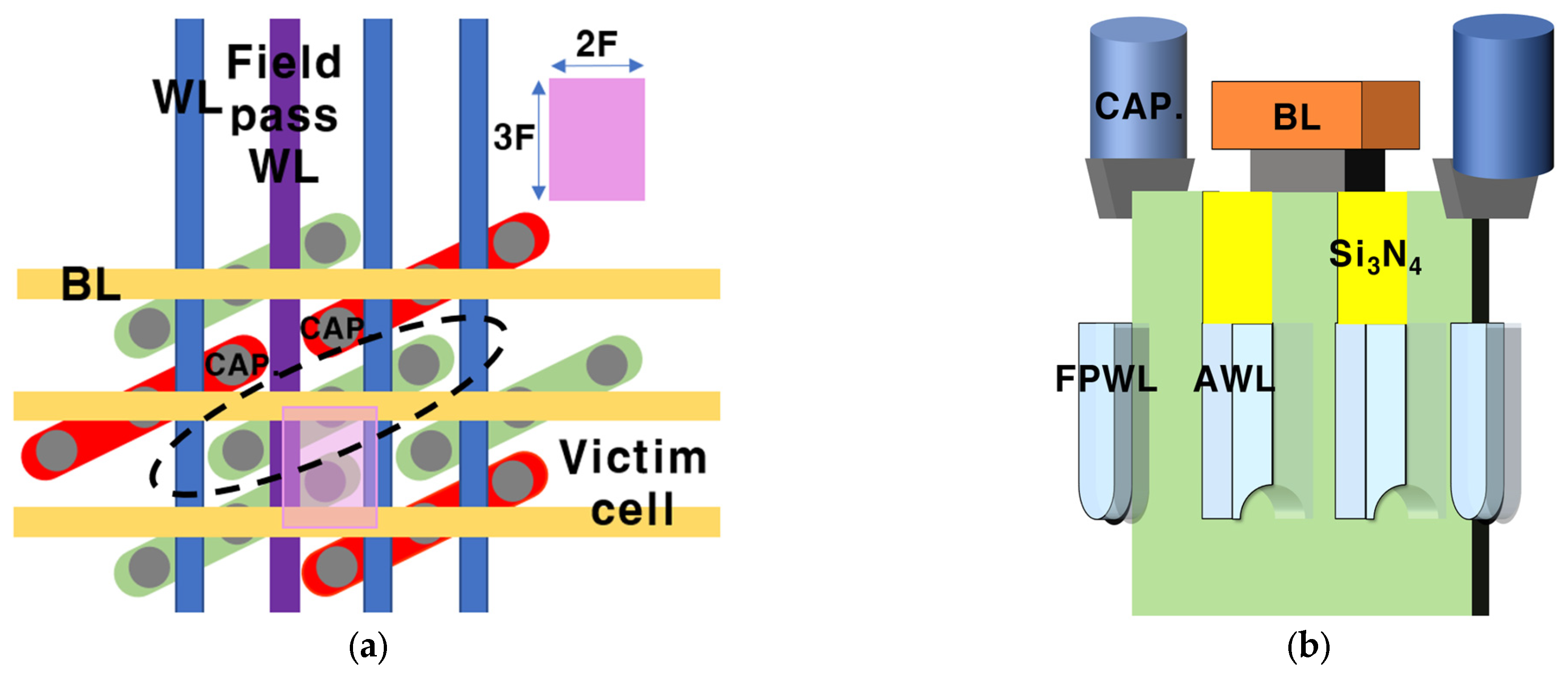
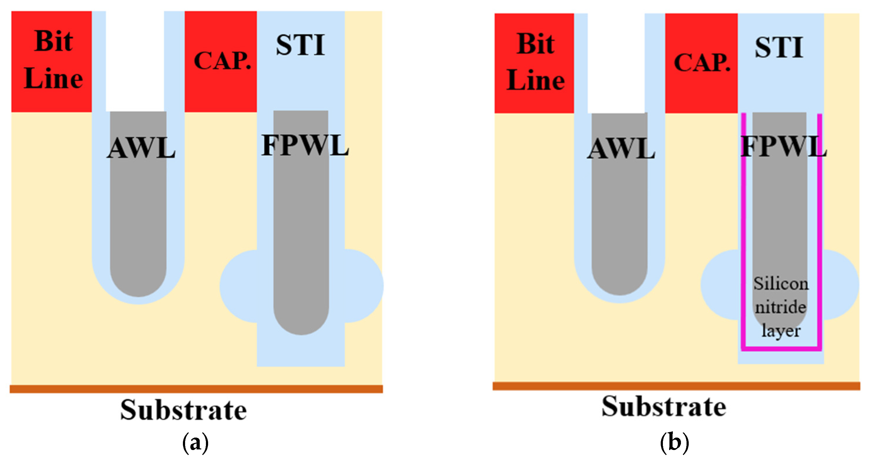
4.1. The Background to Suggesting a Structure

The goal of our study is to propose a structural modification to reduce PGE while keeping the physical separation between AWL and FPWL constant. In Figure 4, it is confirmed that the PGE tended to decrease as the total capacity of the area between AWL and FPWL increased. In the general DRAM, silicon and SiO2 occupy the area between AWL and FPWL. If a DRAM cell is designed simply by increasing the thickness of SiO2, the total capacity increases, and the physical distance between AWL and FPWL increases, thereby naturally alleviating the PGE. However, simply increasing the thickness of SiO2 results in increasing the overall DRAM cell size. This method can certainly improve PGE, but it inhibits the scale-down element, which is one of the important development goals in DRAM at present. Therefore, there is a need for a method of improving PGE while fixing the physical distance between AWL and FPWL. When designing a DRAM by increasing the proportion of SiO2 while the physical distance between AWL and FPWL is fixed, PGE is improved because the total capacity increases. However, simply increasing the proportion of SiO2 will lead to a resistance problem. Increasing the proportion of SiO2 means lowering the proportion of silicon, conversely, reducing the thickness of silicon. As the silicon thickness decreases, the contact resistance between the silicon and the capacitor increases. As a result, the final research goal is to improve PGE by proposing a structure that will not only increase the physical distance between AWL and FPWL but also not increase the contact resistance.

4.2. Proposed Structure

Our proposed structure involves both a partially enlarged spherical STI and a spherical STI with an additional Si3N4 layer. Figure 6a,b show 2D cross-sections of the spherical STI structure and the one with an added Si3N4 layer in the spherical STI, respectively. The spherical STI process can be fabricated through the dry–wet–dry etch process [15]. The spherical STI structure selectively enhances the oxide ratio in a specific area between AWL and FPWL. Spherical STI was adopted to increase the ratio of the dielectric constant of relatively low oxides compared to silicon and not to increase the contact resistance between the silicon and capacitor. Moreover, incorporating a Si3N4 layer within the spherical STI serves to alleviate PGE by enabling charge programming within the Si3N4 layer.

4.3. Simulation Experiment Results

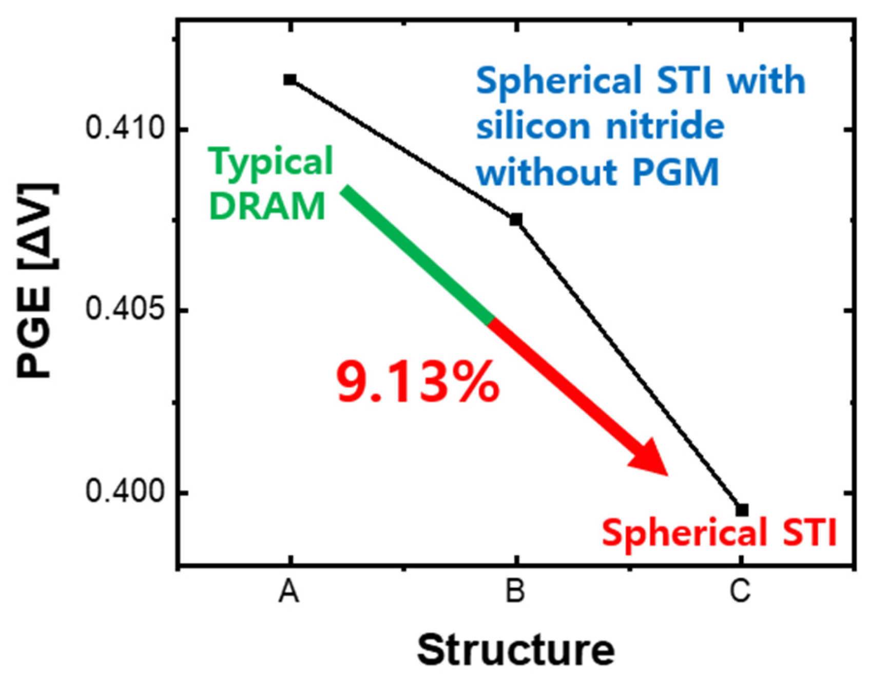
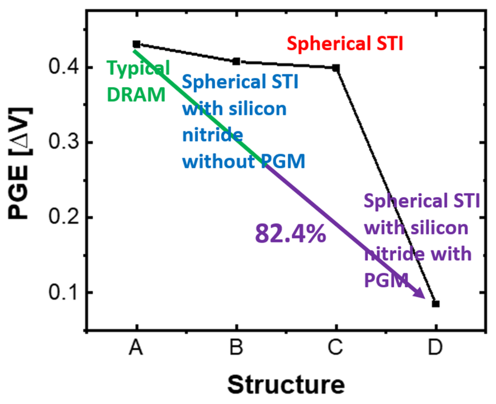
4.3.1. Structural PGE Comparison

Before optimizing the proposed structures, we compared PGE between conventional DRAM and our proposed structures. Figure 7 shows a remarkable similarity to the results discussed in Figure 4. This similarity can be attributed to the difference in dielectric constants between oxide and silicon. The spherical STI structure has a higher proportion of oxides due to spherical STI between AWL and FPWL compared to conventional DRAM. This can result in a lower electric field generated by the voltage of FPWL, affecting the channel of the victim cell. As a result, the higher the proportion of silicon within the silicon-active region, the higher the role the oxide plays in mitigating PGE. In addition, the introduction of Si3N4 layers into conventional DRAM structures has a higher dielectric constant of Si3N4 than of SiO2 and, thus, has a relatively lower total capacitance than standard STIs. However, our proposal using spherical STIs with Si3N4 layer structures effectively prevents the increase in undesirable dielectric constants. Thus, the proposed structure in which Si3N4 layers were added to spherical STIs does not reduce PGE compared to spherical STI structures but shows a decrease in PGE compared to conventional DRAM structures. As a result, we demonstrated that the application of our proposed structure alone induces a decrease in PGE.

4.3.2. Optimization for Spherical STI

We measured the PGE according to the interface trap density of the surface STI further from the spherical STI structure we proposed. The interface trap of the spherical STI affected the Vth of the victim cell, even when the FPWL was turned off. Therefore, in order to observe the effect of PGE according to the interface trap density, we excluded the Vth change due to the surface trap by adjusting the silicon doping concentration of the DRAM cell. Both the general spherical STI and the spherical STI structure to which the surface trap was applied had the same Vth when the FPWL was turned off. We could purely measure the effect of PGE according to the surface trap density under this condition. Figure 8a shows the PGE change according to the trap density. Interestingly, PGE tends to decrease as the trap density increases. We interpreted this phenomenon from the perspective of an energy band. The energy band figure between AWL and FPWL is shown in Figure 3a. At this time, silicon between AWL and FPWL is doped in a p-type, so the Fermi level energy will be formed close to the valance band. Since the p-type concentration of silicon is not very high, there is a distance between the valence band and the Fermi level energy. At this time, if there is an interface trap between the valance band and the Fermi level energy, electrons are captured and present in this interface trap. The condition in which electrons can be captured in the interface trap is possible when the voltage in the off state of the FPWL we tested is higher than the flat band voltage. We found the flat band voltage condition while changing the voltage of the FPWL. As a result, it was confirmed that the flat band condition appears at a voltage relatively lower than the voltage in the FPWL off state in which we experimented. Therefore, even when the FPWL we experimented with is off, electrons can be captured in the interface trap. The negative charge captured in this interface trap causes capacitance coupling between the AWL and the FPWL. As the negative charge increases on the spherical STI surface, the positive charge should increase on the AWL side. The positive charges increased on the AWL side appear as if a positive voltage is applied to the AWL. As a result, the Vth of the victim cell decreases even in the FPWL off state. This brings about the effect of reducing the Vth difference between the FPWL off state and the on state and, finally, shows the effect of improving the PGE. This effect improves the PGE by effectively reducing the Vth difference as the interface trap density increases. Nevertheless, even if the interface trap density increases, there is a section in which the PGE hardly decreases. Electrons sufficiently captured in the interface trap of the spherical STI reduced the voltage interference between FPWL and AWL extremely. Therefore, the trap fish on the spherical STI surface is an important variable affecting PGE.
We further investigated the trend of PGE based on the energy level of the trap present on the sphere STI surface. We improved PGE based on the energy level of the interface trap in sphere STI. Figure 8 shows the PGE change based on the interface trap energy level. As the trap energy level increases, the PGE tends to decrease. The probability of electrons being captured varies depending on the interface trap energy level. The lower the interface trap energy, the easier the electrons are captured by the trap, and the higher the energy, the lower the probability of being captured. However, if the interface trap energy is low, electrons captured in the trap can be easily emitted, and if the energy is high, the probability of emitting electrons captured in the trap decreases. Because of this phenomenon, we observed the change in PGE according to the interface trap energy. As a result, when the interface trap energy level reached its peak, the PGE was the lowest. It was observed that the PGE was lowered in proportion to the interface trap energy level.

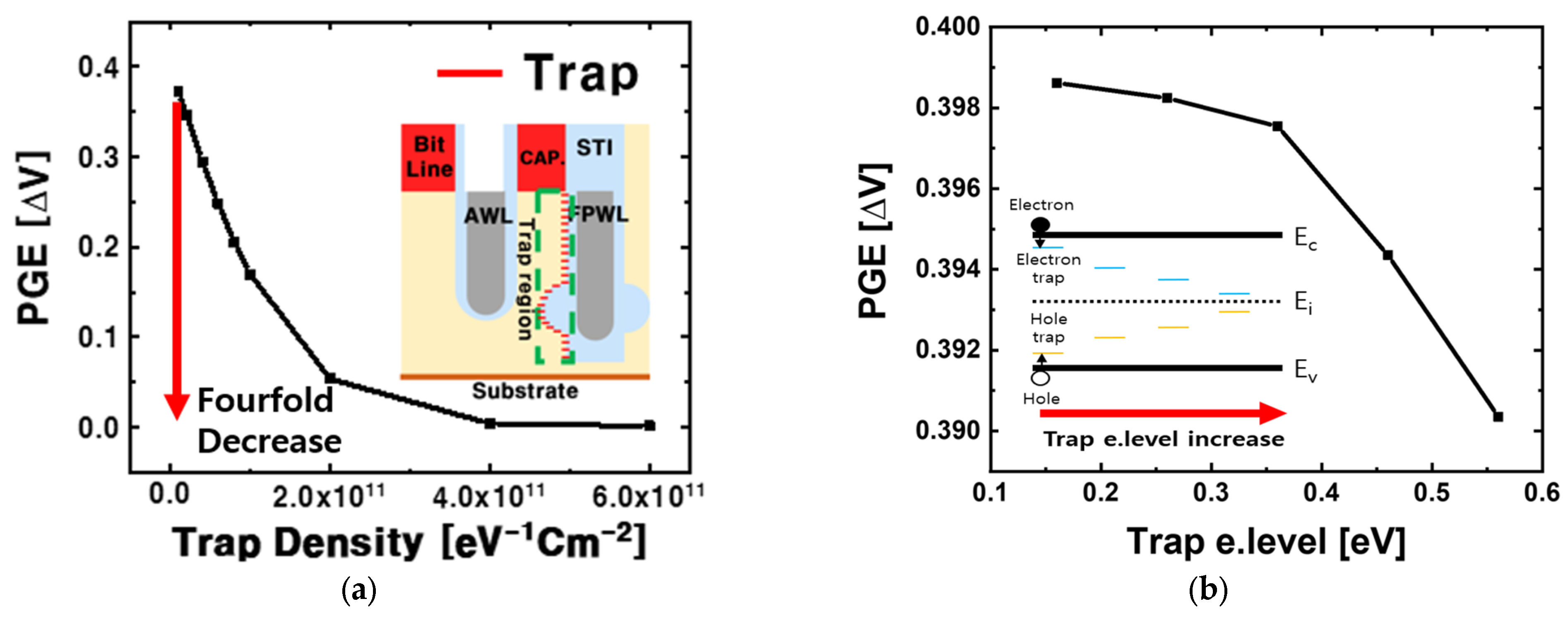
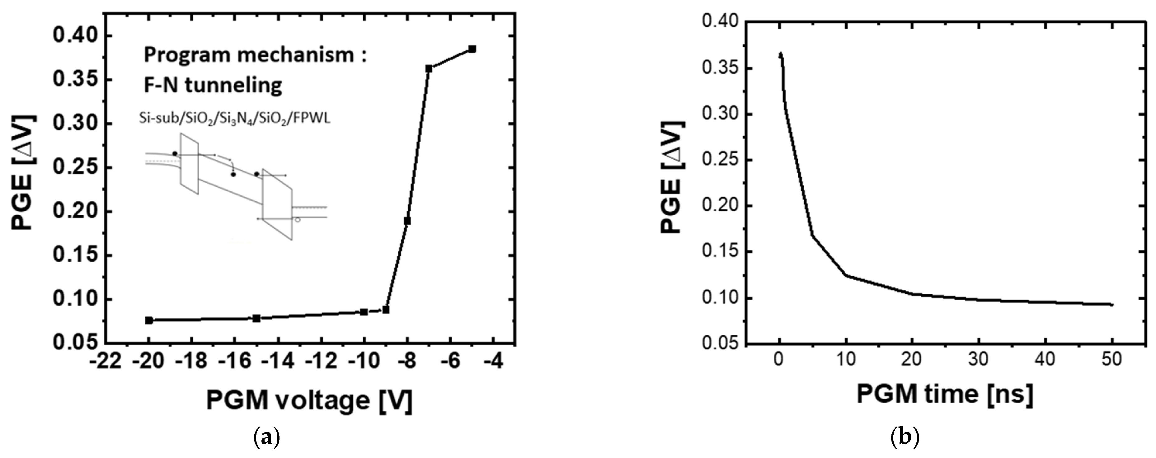
4.3.3. Optimization for Spherical STI with an Added Si3N4 Layer

The interface trap of the spherical STI can certainly play a major role in reducing PGE. However, along with PGE, it can cause 1-row hammer, which is currently the most important problem in DRAM, causing damage to the data stored in the capacitor. Therefore, we propose a structure in which a silicon nitride layer is embedded in the old STI so that it can play a role similar to the interface trap of the old STI. We propose a method of reducing PGE by programming charges in Si3N4. We improved PGE by finding optimal conditions based on the voltage and time when programming charges within the Si3N4 layer of a spherical STI. Figure 9a shows the PGE according to the program voltage. We used the Fowler Nordheim (FN) tunneling mechanism, a mechanism used when charging electrons to Si3N4 in an NADN flash memory. When charging an electric charge using FN tunneling, programming starts when the voltage exceeds a specific threshold. In Figure 9a, it was also confirmed that programming started when it was less than about −10 V and PGE decreased. In addition, the thin oxide between the Si3N4 layers we proposed is a structure that can be programmed on the Si3N4 layer, even at about −10 V.
Furthermore, we optimized the programming time using FN tunneling. Figure 9b shows a reduction in PGE over programming time. The trend toward PGE was observed while changing the programming time from 0 s to 50 ns. From 0 s to about 30 ns, the PGE improved in proportion to the programming time. When the programming time is 30 ns or more, the Si3N4 is sufficiently charged, reducing the width at which PGE decreases. Since the Si3N4 layer we proposed is only 2 nm thick, the charges are sufficiently charged when the programming time is 30 ns or more, thereby improving the PGE.
Figure 10 shows a comparison of PGE after programming the PGE and spherical STI with Si3N4 structures of typical DRAM. As a result of the comparison, it was shown that the PGE of the structure optimized through PGM decreased by 82.4% in the spherical STI with the Si3N4 structure finally proposed through our research results rather than the PGE of typical DRAM. As a result, we verified that the research results were consistent with the purpose of the study.

5. Conclusions

In this study, we employed energy band analysis to investigate the Pass Gate Effect (PGE) in the dynamic random-access memory (DRAM) transistor. Specifically, we aimed to discern the key parameters influencing PGE by examining the dielectric constant’s impact on the widely adopted buried channel array transistor (BCAT) structure. To achieve this, we conducted a systematic examination of PGE tendencies while varying the dielectric constant within the BCAT structure. By doing so, we identified crucial factors that contribute to the emergence of PGE. This analysis allowed us to gain a deeper understanding of the underlying mechanisms responsible for PGE in DRAM transistors. Based on the understanding of the basic mechanism, the PGE phenomenon in this study was analyzed by defining it as the Vth difference of the victim cell. Based on the analysis results, we proposed structural improvements related to the addition of our proposed spherical STI (Shallow Trench Isolation) and silicon nitride film. The proposed spherical STI analyzed the tendency toward PGE and improved PGE in relation to the interface trap density and energy level. In addition, we tried to mitigate PGE by optimizing two important factors of program voltage and timing in the structure in which the silicon nitride film was added to the proposed spherical STI. Using SILVACO simulations, we observed remarkable results. The PGE was substantially reduced by approximately fourfold magnitude when compared to the PGE levels in the typical DRAM BCAT structure currently in widespread use. This impressive reduction signifies the significant impact of our optimizations on PGE mitigation. Our findings not only shed light on the fundamental factors influencing PGE in DRAM but also demonstrate the practical feasibility of our proposed solutions. The substantial reduction in PGE achieved through these optimizations holds great promise for enhancing the reliability and performance of DRAM technology.

Author Contributions

Conceptualization, Y.-S.K. and M.-W.K.; methodology, Y.-S.K.; validation, Y.-S.K. and C.-Y.L.; investigation, Y.-S.K. and C.-Y.L.; resources, Y.-S.K.; writing—original draft preparation, Y.-S.K.; writing—review and editing, Y.-S.K.; visualization, Y.-S.K.; supervision, M.-W.K.; project administration, Y.-S.K., C.-Y.L. and M.-W.K.; funding acquisition, M.-W.K. All authors have read and agreed to the published version of the manuscript.

Funding

This research was supported by the National R&D Program through the National Research Foundation of Korea (NRF) funded by the Ministry of Science and ICT (NRF-2022M3I7A1078936) and this work was supported by the National Research Foundation of Korea (NRF) grant funded by the Korea government (MSIT) (2021R1G1A1093786).

Data Availability Statement

The data presented in this study are available in this article.

Conflicts of Interest

The authors declare no conflict of interest.

References

  1. Sun, Y.; Liu, X.; Wang, N.; Jeon, J.; Wu, B.; Cao, K. Trap-Assisted Passing Word Line Leakage and Variable Retention Time in DRAM. In Proceedings of the 2021 IEEE 4th International Conference on Electronics Technology (ICET), Chengdu, China, 7–10 May 2021. [Google Scholar]
  2. Gautam, S.K.; Manhas, S.K.; Kumar, A.; Pakala, M. Mitigating the passing word line induced soft errors in saddle fin DRAM. IEEE Trans. Electron Devices 2020, 67, 1902–1905. [Google Scholar] [CrossRef]
  3. Han, J.W.; Suh, M.; Lee, G.; Kim, J. Overhang Saddle Fin Sidewall Structure for Highly Reliable DRAM Operation. IEEE Access 2023, 11, 82738–82743. [Google Scholar] [CrossRef]
  4. Yang, T.; Lin, X.W. Trap-assisted DRAM row hammer effect. IEEE Electron. Device Lett. 2019, 40, 391–394. [Google Scholar] [CrossRef]
  5. Woo, J.; Chung, K.S. Mitigating Row-hammering by Adapting the Probability of Additional Row Refresh. In Proceedings of the 2019 IEEE 4th International Conference on Technology, Informatics, Management, Engineering & Environment (TIME-E), Bali, Indonesia, 13–15 November 2019. [Google Scholar]
  6. Kim, D.H.; Nair, P.J.; Qureshi, M.K. Architectural support for mitigating row hammering in DRAM memories. IEEE Computer Archit. Lett. 2014, 14, 9–12. [Google Scholar] [CrossRef]
  7. Son, M.; Park, H. Making DRAM strong against row hammering. In Proceedings of the 2017 54th ACM/EDAC/IEEE Design Automation Conference (DAC), New York, NY, USA, 18–22 June 2017. [Google Scholar] [CrossRef]
  8. Lim, K.Y.; Yu, X.; Yeo, D. A study on gate-induced junction breakdown. In Proceedings of the 2001 6th International Conference on Solid-State and Integrated Circuit Technology. Proceedings, Shanghai, China, 22–25 October 2001. [Google Scholar] [CrossRef]
  9. Lo, G.Q.; Joshi, A.B. Hot-carrier-stress effects on gate-induced drain leakage current in n-channel MOSFETs. IEEE Electron. Device Lett. 1991, 12, 5–7. [Google Scholar] [CrossRef]
  10. Chang, C.; Haddad, S.; Swaminathan, B.; Lien, J. Drain-avalanche and hole-trapping induced gate leakage in thin-oxide MOS device. IEEE Electron. Device Lett. 1988, 9, 588–590. [Google Scholar] [CrossRef]
  11. Yuan, X.; Park, J.E.; Wang, J.; Zhao, E.; Ahlgren, D.C.; Hook, T.; Yuan, J.; Chan, V.W.C.; Liang, C.-H. Gate-Induced-Drain-Leakage Current in 45-nm CMOS Technology. IEEE Trans. Device Mater. Reliab. 2008, 8, 501–508. [Google Scholar] [CrossRef]
  12. Lin, Y.; Wolf, J.K. Combined ECC/RLL code. IEEE Trans. Magn. 1998, 24, 2527–2529. [Google Scholar] [CrossRef]
  13. Kwon, S.; Son, Y.H.; Ahn, J.H. Understanding DDR4 in pursuit of In-DRAM ECC. In Proceedings of the 2014 International SoC Design Conference (ISOCC), Jeju, Republic of Korea, 3–6 November 2014. [Google Scholar] [CrossRef]
  14. Yamada, T.; Kotani, H.; Matsushima, J.; Inoue, M. A 4-Mbit DRAM with 16-bit concurrent ECC. IEEE J. Solid-State Circuits 1988, 23, 20–26. [Google Scholar] [CrossRef]
  15. Kim, Y.S.; Lim, C.Y.; Kwon, M.W. Reduction of the Pass Gate Effect with a Spherical Shallow Trench Isolation in the BCAT Structure. J. Semicond. Technol. Sci. 2023, 23, 236–242. [Google Scholar] [CrossRef]
Figure 1. (a) DRAM array diagram. Diagram of 6F2 DRAM array top view and relative position of field pass gate and victim cells. (b) DRAM 3D BCAT structure: 3D BCAT structure cross view used for transistor simulation. This structure shows a view of the black dash circle region.
Electronics 13 00681 g001
Figure 2. DRAM 2D BCAT structure. Cross half section of 2D BCAT structure. The saddle fin structure was implemented through the difference in depth between AWL and FPWL.
Electronics 13 00681 g002
Figure 3. (a) AWL and FPWL band energy graph. The simulation results of 2D BCAT structure: band diagram along the red dashed cut lines in Figure 2. (b) IdVg characteristic graph of DRAM. The simulation results of 2D BCAT structure: IdVg curve. We defined the voltage difference at the point of 10−7 current as PGE.
Electronics 13 00681 g003
Figure 4. PGE graph according to dielectric constant. This graph illustrates the direct relationship between dielectric constant and PGE. As the dielectric constant increases, PGE also increases proportionally. In essence, a lower dielectric constant between AWL and FPWL material reduces PGE.
Electronics 13 00681 g004
Figure 5. (a) A mathematical formula of total capacitance and equivalent circuit. The area surrounded by the red dotted line is where the PGE occurs. (b) PGE graph according to ideal capacitance mathematical formula. The graph shows the correlation between dielectric constant and PGE, calculated using the ideal capacitance equation depicted in Figure 5a. Concurrently, graph shows a similar trend of elevated PGE corresponding to the graph illustrated in Figure 4, as the dielectric constant demonstrates an increase.
Electronics 13 00681 g005
Figure 6. (a) Proposed spherical STI structure. We propose the spherical STI structure to increase the proportion of oxide in a targeted region. (b) Proposed spherical STI with Si3N4 structure. We propose the spherical STI structure with a Si3N4 layer to mitigate PGE through programming.
Electronics 13 00681 g006
Figure 7. PGE comparison graph with structure in DRAM. This graph compares the PGE of the typical DRAM structure with two proposed structures when structurally optimized for the typical DRAM structure only. It shows that the proposed Spherical STI structure reduced PGE by approximately 9.13% compared to the typical DRAM structure.
Electronics 13 00681 g007
Figure 8. (a) PGE graph according to the surface trap density of a spherical STI. As the interface trap density increases, the PGE tends to improve. When the interface trap density increases above a certain level, the PGE does not decrease any more. (b) PGE graph according to the surface trap energy level of a spherical STI. This graph illustrates the variation in PGE according to the energy level of traps on the surface of our proposed spherical STI structure. The density of the interface trap, 1011 eV−1 cm−2, was applied to the green dotted area and simulated by changing the trap energy level afterwards.
Electronics 13 00681 g008
Figure 9. (a) PGE graph according to the program voltage. This graph illustrates PGE as a function of program voltage. The programming process is achieved through Fowler–Nordheim (F-N) tunneling. (b) PGE graph according to the program time. This graph shows PGE according to program time. The program time needs to be at least 30 ns to ensure that charges are adequately accumulated in the Si3N4, resulting in a reduction in PGE.
Electronics 13 00681 g009
Figure 10. PGE Comparison graph according to typical DRAM and proposed DRAM structure. This graph compares the PGE of a typical DRAM structure with the two proposed structures when optimized through programming in the proposed structure.
Electronics 13 00681 g010
Table 1. Structure dimension and simulation condition.
Structure Condition[nm]Simulation ConditionVoltage [V]
Gate oxide thickness side/bottom (Tox,side/Tox,bot)8/6BL voltage1
Silicon active width (Wsi)23Silicon active WL voltage (Von/Voff)3/−0.2
Shallow trench isolation width (WSTI)28Field Pass WL voltage (Von/Voff)3/−0.2
Word line width
(WAWL, WFPWL)
12Substrate voltage−0.6
Fin depth
(DFin)
20
Disclaimer/Publisher’s Note: The statements, opinions and data contained in all publications are solely those of the individual author(s) and contributor(s) and not of MDPI and/or the editor(s). MDPI and/or the editor(s) disclaim responsibility for any injury to people or property resulting from any ideas, methods, instructions or products referred to in the content.

