Abstract
Information is pivotal in contemporary society, highlighting the necessity for a secure cryptographic system. The emergence of quantum algorithms and the swift advancement of specialized quantum computers will render traditional cryptography susceptible to quantum attacks in the foreseeable future. The lattice-based Saber key encapsulation protocol holds significant value in cryptographic research and practical applications. In this paper, we propose three types of polynomial multipliers for various application scenarios including lightweight Schoolbook multiplier, high-throughput multiplier based on the TMVP-Schoolbook algorithm and improved pipelined NTT multiplier. Other principal modules of Saber are designed encompassing the hash function module, sampling module and functional submodule. Based on our proposed multiplier, we implement the overall hardware circuits of the Saber key encapsulation protocol. Experimental results demonstrate that our overall hardware circuits have different advantages. Our lightweight implementation has minimal resource consumption. Our high-throughput implementation only needs 23.28 s to complete the whole process, which is the fastest among the existing works. The throughput rate is 10,988 Kbps and the frequency is 416 MHz. Our hardware implementation based on the improved pipelined NTT multiplier achieved a good balance between area and performance. The overall frequency can reach 357 MHz.
1. Introduction
Information is fundamental in modern society, demanding secure cryptographic systems for protection. Traditional cryptographic systems rely on mathematical problems that are computationally hard within a finite polynomial time [1,2]. For instance, the RSA public key encryption algorithm relies on the hardness of integer factorization to ensure the security of its private key [3]. However, with the emergence of quantum algorithms and the rapid development of specialized quantum computers, it is expected that traditional cryptography will be vulnerable to quantum attacks in the foreseeable future [4]. Post-quantum cryptographic algorithms, such as CRYSTALS-Kyber, are standardized as the new generation of cryptographic protocols designed to resist quantum attacks [5]. Similarly, the Saber key encapsulation protocol, which is based on lattice problems [6,7], holds substantial value for both research and practical applications in cryptography.
In the third round of evaluation by the National Institute of Standards and Technology (NIST), failure to update the security of Saber with parameter sets to counter the DualAttack led to inferior RAM model security in software compared to Kyber. Although eliminated by NIST, the Saber algorithm retains valuable attributes suitable for research and implementation in academic and industrial settings [8]. Therefore, this study chooses the Saber algorithm for the overall hardware implementation of the protocol. The research provides valuable insights for the future deployment of Post-Quantum Cryptography (PQC) in various scenarios [9]. This is particularly important given the growing global concern about the threat of quantum attacks. While Saber is no longer a standard of NIST, it remains an algorithm that boasts clear advantages in hardware implementation, transmission bandwidth and robust security. Overall, the ongoing research into the Saber algorithm continues to hold significance and meaning, particularly within specialized fields.
This paper focuses on the hardware design and implementation of the Saber key encapsulation protocol. In 2017, Jan-Pieter et al. designed the first version of the Saber key encapsulation protocol and submitted it to NIST [10]. The main operation of the Saber algorithm involves the multiplication of a ring polynomial matrix and a vector in the modular domain. The NTT algorithm demonstrates commendable hardware performance, effectively addressing the polynomial multiplication requirements of KEM schemes rooted in the M-LWE or LWE problem [11]. Polynomial multiplication is no longer the primary bottleneck in this context. The key bottleneck lies in the functions responsible for key generation. These functions exhibit significant latency and consume considerable hardware resources, necessitating optimization efforts.
Hardware implementation has a clear speed advantage due to its high level of parallelism. As a result, numerous researchers both domestically and internationally, have utilized FPGA platforms and ASICs. In 2020, Sujoy Sinha Roy et al. designed the first hardware implementation of the Saber algorithm using Xilinx’s Zynq UltraScale FPGA platform [12]. In order to expedite polynomial multiplication, the author employed 256 low-level operators simultaneously, leading to the Schoolbook algorithm being completed in 256 cycles. This approach effectively resolves the memory access bottleneck with minimal impact on the overall area. The co-processing architecture is adopted, and a customized 32-bit instruction set is used for operator control, considering both flexibility and performance. The peripheral control circuit of the SHA3 function is optimized simultaneously [13]. The hardware results show that the frequency reaches 250 MHz, and only 23.6 k LUT resources are consumed. In 2022, Zhu et al. implemented the Saber algorithm using the TSMC 28 nm process. The overall chip area is only 3.6 mm2, and it operates at a frequency of 500 MHz. This is also the first complete implementation of the Saber protocol of ASIC and has been verified by a fluidic chip. The ASIC implementation is superior to other cryptographic algorithms in terms of power consumption and security [14]. Andrea Basso et al. implemented the multiplication of Saber and Dilithium on Artix-7 in 2021 using the same iterative NTT polynomial multiplier. This implementation consumed 519 clock cycles, which is lower compared to the NTT multipliers used in other cryptographic algorithms [15]. In addition, Aikata et al. designed a unified coprocessor architecture that can implement both Dilithium and Saber [16]. They aligned the data stream of hash function output random numbers and conducted a thorough analysis of the impact of the bit width of polynomial coefficients on the results of NTT. VietBaDang et al. presented a high-performance benchmark implementation of the Saber, Kyber and NTRU algorithms [17]. By integrating and optimizing existing implementations, they determined that the Saber protocol at medium security levels can be completed in 48.4 s. Rentería-Mejía et al. presented the design of LWE cryptoprocessors utilizing NTT cores and Gaussian samplers based on the inverse transform method. The cryptoprocessors were synthesized on a field-programmable gate array and subsequently validated in hardware, which exhibits noteworthy throughput [18]. In continued research, they proposed a lattice-based encryption scheme for Identity-Based Encryption, alongside a lattice-based cryptoprocessor tailored for the encryption or decryption of the suggested CCA Identity-Based Encryption scheme, specifically for security parameters n = 512 and n = 1024. The hardware implementation demonstrated efficiency, achieving a commendable level of throughput [19].
In this paper, we propose three types of polynomial multipliers for various application scenarios including the lightweight Schoolbook multiplier, high-throughput multiplier based on TMVP-Schoolbook algorithm and improved pipelined NTT multiplier. Other principal modules of the Saber protocol are designed, encompassing the hash function module, sampling module and functional submodule. Based on our proposed multiplier, we implement the overall hardware circuits of the Saber key encapsulation protocol. Experimental results demonstrate that our overall hardware circuits have different advantages compared with other existing works.
The following sections outline the structure of this paper. In Section 2, we provide a description of the Saber key encapsulation protocol. In Section 3, we propose three types of polynomial multipliers for various application scenarios including lightweight Schoolbook multiplier, high-throughput multiplier based on TMVP-Schoolbook algorithm and improved pipelined NTT multiplier. Moreover, other principal modules of Saber are designed, encompassing the hash function module, sampling module and functional submodule. In Section 4, we implement the overall hardware circuits of the Saber key encapsulation protocol based on our proposed multiplier. In Section 5, we analyze the results and compare with other existing works. Finally, we make a conclusion and reflect on future work in Section 6.
2. Preliminaries
The Saber key encapsulation protocol is described in Algorithms 1–3 including key generation, key encapsulation and key decapsulation [20].
| Algorithm 1 KEM.KeyGen() |
|
In the key generation phase, step 1 involves invoking the function from the public key encryption algorithm to generate a public-private key pair (, ) with IND-CPA security level [21]. The public key undergoes a hash function, specifically SHA3-256, to obtain a 256-bit message digest, which is the hashed value of with the public key information. In Step 3, z represents a 256-bit random number generated by uniform sampling. Its purpose is to generate a random value in case of decryption failure. The operator performs bitwise concatenation, which does not consume any resources.
| Algorithm 2 KEM.Encap() |
|
The key encapsulation phase aims to obtain the public key from the key generation phase and generate a session key. This phase also includes generating a ciphertext that contains the random seed used to generate the session key. Unlike public key encryption, there is no plaintext involved in the encryption process. The 256-bit message m is also obtained by sampling from a uniform distribution and then hashed using a hash function to obtain . The public key is hashed to obtain , which is then concatenated with to form a 512-bit hash value. The upper 256 bits of the hash value are utilized as input for generating the random number r in Step 5, while invoking the public key encryption function. This process results in an IND-CCA secure ciphertext called . The session key is generated through two rounds of SHA3-256, and it is stored by the server [22]. Once the communication is closed, the session key is deleted, effectively protecting the key.
| Algorithm 3 KEM.Decap() |
|
In the decapsulation phase, the ciphertext received along with the private key from the key generation phase, is used to derive the session key corresponding to the ciphertext. The message m is obtained by decrypting the received . Then, m is concatenated with the hash value of to form a 512-bit . In Step 6, the public key encryption algorithm is invoked again to generate the ciphertext on the client side. The next step is to verify whether the client’s ciphertext matches the server’s ciphertext. If they do not match, the output is , and if they do match, the output is . The session key is then returned.
3. Proposed Design
3.1. Hardware Implementation of Polynomial Multiplier
3.1.1. Lightweight Schoolbook Polynomial Multiplier
The polynomial multiplier consumes most of the resources in the hardware implementation of Saber [23], which needs to be optimized for efficient hardware implementation. In the previous work [24], we have designed a lightweight and efficient Schoolbook polynomial multiplier for Saber. The architecture includes an efficient multiplication strategy, enabling the computation of four coefficient-wise multiplications per cycle along with the multiplication operand loading technique being designed for the compact multiplier. The hardware architecture of the lightweight Schoolbook multiplier, as shown in Figure 1, consists of several main components: a public polynomial data loading module, a control module, two DSP units, four either multiplexers, four 13-bit accumulation registers, and four adders. RAM_A serves as the storage BRAM unit for the entire protocol, enabling immediate updates and overwriting unnecessary intermediate data, thereby conserving resources. RAM_S, also a true dual-port BRAM, has a bit width of 4 bits and an address depth of 786. In fact, if three lightweight multipliers are instantiated simultaneously and operate in the same multiplication state and progress, they can share the output data from a single RAM_S, reducing the required cycles for multiplication in the protocol and improving throughput. During the multiplication computation, coefficients of the same order are computed first, and then higher-order coefficients are calculated sequentially in a serial manner. This approach enables the accumulation of new partial product results within a restricted number of registers, considering the resource constraints in each cycle of the lightweight implementation. The designed Schoolbook polynomial multiplier demonstrates scalability, allowing for flexibility in its configuration. This adaptability is achieved through the manipulation of the algorithm’s cycle count and the adjustment of bit width during the operational process. The polynomial data loading module is dynamically modified, introducing an additional stage to facilitate seamless integration with architectures of varying sizes, specifically accommodating either a 512-point or a 1024-point architecture.
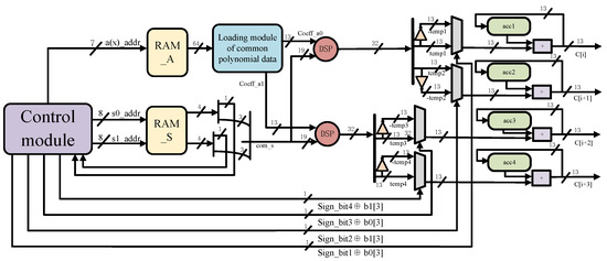
Figure 1.
Lightweight Schoolbook polynomial multiplier [18].
The multiplier receives input and generates an output signal. The control module updates the address in each cycle. It reads the corresponding coefficient through the three address lines: s0_addr, s1_addr, and a(x)_addr. RAM_A 64 outputs data flow through the polynomial of the data load module, resulting in two streams of 2nd order difference coefficient flow: Coeff_a1 and Coeff_a0. These signals are combined with the 19 com_s signals and then multiplied by the two DSPs. A single DSP48E1 unit can handle signed multiplication with a bit width of 25 × 18. Therefore, in the case of Saber, two point-to-point unsigned multiplications can be executed simultaneously, enabling the multiplier to perform four multiplications in a single cycle. This enhances parallelism. The upper 16 bits and the lower 16 bits of the 32-bit output of the DSP (with 30 bits that will not overflow), respectively, represent the absolute value of a partial product. In this case, we need to match the four partial products with the four coefficients that correspond to the multiplication result. Because the modules of Saber are all powers of 2, the modular reduction operation can be completed by intercepting only the 16 bits and the lower 13 bits in the hardware implementation, without consuming excessive resources for modular reduction. The addition or subtraction of the value in the accumulation register is determined by the pre-calculated sign bit and the original sign phase of the secret polynomial coefficient. The output result is produced after 256 cycles, without an explicit result write-back cycle. The global multiplier does not have any redundant clock cycles, except for a few cycles that are initialized. After 16,384 cycles, the single polynomial multiplication is completed.
3.1.2. High-Throughput Polynomial Multiplier Based on TMVP-Schoolbook
As illustrated in Figure 2, the proposed high-throughput polynomial multiplier is specifically designed for Saber based on the TMVP-Schoolbook algorithm. At the start of the multiplication process, the multiplier initially retrieves the coefficients of the secret polynomial from an external BRAM and stores them in the buffer. Once loaded, it performs left cyclic shift operations on the coefficients in the buffer during each cycle [25]. It sequentially loads groups of 4 bits into the underlying 256 computational units. The coefficient loading module for the public polynomial simultaneously reads four coefficients, each separated by 64 degrees. It then generates their multiples in the centralized multiplier, which are subsequently inputted into the underlying computing units. The absolute values of the coefficients in the secret polynomial serve as control bits for the four selectors in each computing unit, selecting the corresponding sjai. During subtraction, the additive inverse of the coefficient is computed in the finite field before performing the addition operation. To further increase the efficiency of the multiplier, registers are inserted at the blue dotted line, implementing a three-stage pipeline [26]. The multiplier is controlled by a finite state machine, and the top-level module includes an Acc_clear signal that determines whether the 3328-bit accumulation registers should be cleared. This optimization can be performed during the initial multiplication of the matrix polynomial to reduce the number of cycles required for writing back two-thirds of the multiplication results and reading the previous multiplication results. The TMVP-Schoolbook polynomial multiplier, as designed, is parametrizable. According to the specific requirements of the bit width, it possesses the capability to dynamically retrieve coefficients of the polynomial multiplier, making it adaptable for various architectures with different parameters.
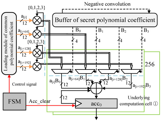
Figure 2.
Proposed high-throughput polynomial multiplier based on TMVP-Schoolbook.
3.1.3. Improved Pipelined NTT Polynomial Multiplier
For the Saber algorithm, a prime number with a module of 23 bits is selected as the new module where [27]. As shown in Table 1, there are the NTT/INTT parameters for the Saber algorithm.

Table 1.
Parameters of NTT/INTT for Saber.
The modulo multiplier circuit needs to reduce the result obtained by multiplying two 23-bit numbers back to a 23-bit number. Since the modulo is a prime, an iterative modulo reduction algorithm can be constructed iteratively using the congruence property of . Firstly, the range of a 45-bit signed number is , which is sufficient to multiply two numbers in the range of without causing overflow. Therefore, the temporary bit of the product is 45-bit. Then we can obtain the following:
In Equation (4), is the lowest 13-bit, is the middle 10-bit, and is the highest 2-bit. These discrete bits correspond to the coefficients extracted from the formula. The main idea is to approximate t from by simple shifts and additions and subtraction, and then make a fine final adjustment. The final output result will be in the range of . It is noted that the reduced values will not be strictly evenly distributed in the range of . Most of the values will be far away from the boundary values, which roughly corresponds to a normal distribution. In addition, there is a modular reduction algorithm to consider. It involves reducing the 45-bit product into an unsigned number and separately recording the sign bits. The unsigned number reduction algorithm is used to reduce the value, and the final result will be in the range of .
The proposed overall modulo multiplier circuit is replaced by the power multiplication of 2 using the left shift operation in Figure 3. The remaining components mainly consist of addition, subtraction, and a comparator. To improve frequency, the modulo multiplier unit is divided into four pipeline stages, as it serves as the underlying module for NTT transformation and can limit overall performance. Moreover, in order to minimize the path length and resource consumption, one of the three-input adders is replaced by 10-bit carry-save adders. The NTT polynomial multiplier, designed with a radix-2 architecture, is easily scalable. Transitioning from a 256-point architecture to 512 points requires only a single additional stage, and for a 1024-point architecture, just two additional stages are needed. The implementation is both straightforward and minimally demanding in terms of hardware resources.
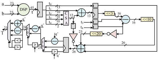
Figure 3.
Proposed NTT modulo multiplier circuit.
3.2. Hardware Implementation of SHA-3 Hash Function Module
3.2.1. Permutation Iterative Wheel Function
SHA-3 is a cryptographic hash function introduced by NIST through a standardization competition in its early stages [28]. It is capable of generating random numbers of any length and provides resistance against collision attacks and second pre-image attacks. In other words, knowing the hash value does not reveal the input message, and the hash values of any two message sets will not be identical. Currently, the most advanced attack methods can only target the fourth or fifth rounds of the iterative operation of SHA-3 functions. Therefore, SHA-3 functions are considered highly secure for applications such as message digests and pseudo-random number generation. Hash functions are widely used nowadays, and the lattice-based cryptographic key encapsulation protocol has chosen SHA-3 functions as a generator of a large number of pseudo-random numbers and as a message digest function to reduce transmission bandwidth while enhancing security.
The Saber key encapsulation protocol utilizes the extensible functions SHAKE-128, SHA3-256 and SHA3-512. SHAKE-128 serves as a sampling algorithm for polynomial coefficients, capable of generating pseudo-random numbers of any length. The hash functions SHA3-256 and SHA3-512 are used for hashing and protecting public and private keys. They generate 256-bit and 512-bit hash values for messages of any length. Regardless of the specific function used, they all share an internal iteration function called Keccak, which is controlled by different parameters in the external control logic. Therefore, optimizing the performance of the Keccak function is crucial to ensure efficient operation of the hash module and prevent it from becoming a bottleneck in the overall protocol circuit. In [19], two hash function cores are designed based on the SHA3-256 and SHAKE256 functions for CCA-secure Identity-Based Encryption, which inserts two registers in the Keccak function. The architecture can simultaneously process multiple rounds of data, demonstrating high performance. In this study, we implement the circuit of the Keccak function by pure combinatorial logic without any pipelined designs. We design a dedicated hash function structure for the Saber algorithm to achieve remarkable performance.
The Keccak iteration function consists of 24 rounds of the round function KECCAK-f[1600]. Each round of the function performs a series of operations, including permutation, XOR, and iteration on 1600-bit data. The 1600-bit data are derived from the state matrix A in three-dimensional space. The round function is divided into five steps, which correspond to five sub-functions. In the round function, it inputs the state matrix A and outputs the state matrix . Here are the five steps:
In the five steps mentioned above, the ranges for x and y are 0 to 4, while the range for z is 0 to 63. The value of varies based on the round number and is a 64-bit number. It can be observed that most of the internal steps within the round function involve simple shift or XOR operations, which are relatively straightforward and friendly to hardware. As a result, even without specific optimization techniques, the implementation of KECCAK-f[1600] demonstrates excellent performance. Therefore, this paper presents the hardware circuit depicted in Figure 4. The circuit is implemented using pure combinatorial logic without incorporating any pipelining design. The output of the previous sub-function directly feeds into the next sub-function, and the five sub-functions are serially cascaded to form one round. Unlike the other literature, this study does not involve simultaneous processing of data from multiple rounds, resulting in a parallelism factor of 1. The circuit of the round function processes 1600-bit data in one cycle, meaning that one round is completed within a single cycle, and the KECCAK-f operation requires 24 cycles. The overall circuit synthesis result is 2281 LUTs, consuming a reasonable amount of resources.
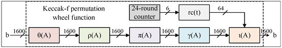
Figure 4.
The hardware circuit diagram of KECCAK-f[1600].
3.2.2. External Overall Control Logic
Utilizing the Keccak permutation function as a foundation, diverse SHA-3 functions can be constructed by configuring different parameters through the sponge construction . In the sponge construction, N represents the input message to the iteration function, d is the length of the message digest and r is the bitrate which varies depending on the function. The capacity c (twice the output message length, c = 2d) is concatenated with r to form a 1600-bit value that is . The sponge construction consists of three stages. The first stage is message padding named pad, where the original input message is first processed with endian conversion. One ‘1’ is then appended to the least significant bit of the bit stream, followed by a variable number of ‘0’s and a final ‘1’. The padding must be positioned at the end of the original message, and the resulting data stream N after padding should be an integer multiple of the bitrate. The rules for pre-processing are shown in the equation as follows. It adds ‘01’ or ‘1111’ after the original message M to form N, depending on the specific function.
After the message padding stage, the next phase is message absorption. The processed message is divided into groups of the bitrate length, forming an integer multiple of the bitrate. The KECCAK-f iteration function absorbs a group of messages after completing 24 rounds of iteration, and the incoming message needs to be XORed with the high r bits of the data currently being processed. Once the messages are fully absorbed, the squeezing phase begins. In this phase, the iteration function is again used to output the message digest. If the desired data length d is shorter than the bitrate r, the high d bits are directly taken. However, if the desired data length is greater than the bitrate, multiple rounds of iteration are performed, with each round producing the high r bits to form the message digest. For example, when generating a 256-bit random seed, SHAKE-128 requires only one round of squeezing, while generating polynomial coefficients with SHAKE-128 requires multiple rounds. After analyzing the protocol, the peripheral circuit designed based on the Keccak core as the underlying iteration function is shown in Figure 5.
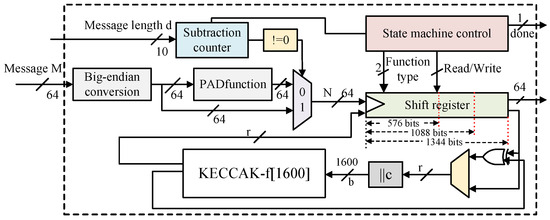
Figure 5.
Hash function module circuit.
The message M is inputted into the SHA-3 module as a 64-bit serial data stream. At the same time, the module is informed of the length of the input data, which is assigned as the initial value of the subtraction counter. The module is also configured with parameters for the hash function, including r, c, and the padding constants. The original message M is converted to a little-endian format. When the subtraction counter reaches 0, message padding is performed, and the data are then entered into a shift register buffer. The buffer checks for empty/full conditions based on the configured bitrate parameter and XORs the r-bit data being iterated in KECCAK-f for message absorption. After being concatenated with the capacity to form b, the data enter the iteration function for computation. In the data writeback stage of squeezing, the data output by the iteration function is assigned to the shift register and serially output as a 64-bit stream. When the desired output data length is reached, the “” signal is raised, and the internal registers are cleared, thus achieving the implementation of three hash functions using a Keccak core in conjunction with peripheral circuitry.
In the Saber protocol, when the security level is considered medium, the input data length for SHA3-256 is divided into four categories: 64 bytes, 128 bytes, 992 bytes and 1088 bytes. During the sixth round of iteration in the KECCAK-f function, it is possible to simultaneously read the data for the next round, saving some of the cycle overhead for data retrieval. In the data output stage, only SHAKE-128 in Saber requires multiple iterations of the iteration function. For serially outputting 64 bits from a total of 1344 bits, it takes 21 cycles. Therefore, it is possible to perform the iteration function simultaneously during the output stage. The time cost of the hash function can be considered as 24 × n cycles, where n represents the number of iterations.
The overall circuit is controlled by a finite-state machine. Under the default circuit synthesis strategy, the main clock is constrained to a period of 2.4 ns without any timing violations. This indicates that the hash function module does not become a bottleneck, even for the fastest 416 MHz frequency multiplier. The circuit consumes 5088 LUTs and 3068 FFs in terms of resources.
3.3. Hardware Implementation of Functional Submodule
3.3.1. Binomial Distribution Sampling
Lattice-based cryptography requires sampling from an error distribution. In the case of R-LWE, a Gaussian distribution is used. However, this approach suffers from the drawback of variable sampling time, which makes it susceptible to timing attacks. With the emergence of LWE problem variants such as M-LWE and M-LWR, the centered binomial distribution has become the preferred choice. The centered binomial distribution is an approximation of the Gaussian distribution and offers lower resource consumption while providing resilience against side-channel attacks. In the Saber protocol, the coefficients of the secret polynomial are primarily constructed using the binomial distribution. The specific method involves grouping the pseudorandom numbers generated by SHAKE-128, which follow a uniform distribution into groups of size . The Hamming weight of the first bits and the last bits, which represent the number of bits equal to 1, is calculated separately. The lower Hamming weight is then subtracted from the higher Hamming weight. The resulting values are constrained within the range of [, ]. The specification of the Saber algorithm mentions that it allows for efficient multiplication of large numbers by small numbers, which facilitates circuit implementation.
Based on the security levels from high to low, is set to 6, 8 and 10. For the medium-security level Saber-768 chosen in this paper, the coefficient range is limited to . Therefore, a 4-bit binary complement representation is sufficient. However, for subsequent polynomial multiplication, we suggest converting the complement representation of the two to a sign-magnitude representation. The representation consists of a sign bit and the absolute value, which is also represented in 4 bits. The advantage of this representation is that the sign bit can be separated from the multiplication during the polynomial multiplication process. Additionally, considering that the secret polynomial coefficients in the NTT multiplier are represented as signed numbers during the NTT transform, a multiplexer can be used to select the corresponding data for inputting into the cache output. Therefore, by using a sign-magnitude representation and employing a multiplexer, the Saber protocol ensures compatibility between the polynomial multiplication process and the NTT multiplier, facilitating efficient operations such as Polynomial Weight Multiplication.
The sampling circuit design is illustrated in Figure 6. The sampling module retrieves 64-bit word blocks from the BRAM storage unit, housing pseudo-random numbers. Conveniently, these 64 bits are divided into eight groups for binary sampling. The eight resulting coefficients, represented in two’s complement form, undergo conversion to sign-magnitude representation through the encoding circuit. The obtained 32-bit data are temporarily stored in a 64-bit buffer cache. In the next cycle, after filling the remaining 32 bits of the buffer, various scenarios occur. The data can either be parallelly outputted to BRAM or serialized for shifting. Serial shifting is necessary because the lightweight Schoolbook multiplier directly indexes the coefficients of the secret polynomial, and the NTT transform also requires a coefficient flow of 4 bits. Although serial output increases the cycle count, it can work in parallel with the squeezing cycles of SHAKE-128, effectively reducing the additional cycle overhead. The overall circuit is controlled by a state machine. The start flag of the sampling module signifies the effective cycle when the upstream module’s pseudo-random data stream begins.
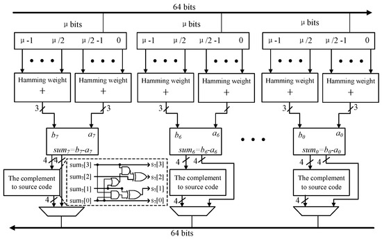
Figure 6.
Binomial distribution sampling circuit.
3.3.2. Remaining Submodules
In addition to the main polynomial multiplication module, hash function, and sampling module, the Saber protocol includes several functional sub-modules with a time complexity of O(n) to ensure the overall completeness of the protocol and reduce the bandwidth requirements. These functional sub-modules combine specific steps outlined in the Saber specification into a single module to improve efficiency. Specifically, these sub-modules include the coefficient packing/unpacking module, the module for adding a constant h1, the module for encryption in the public key primitive, the module for decryption, and the module for verification.
The module is responsible for multiplying a polynomial matrix by a vector, adding the constant h1 = 4 to each coefficient, and then reducing the result modulo the range of . The purpose of the module is to unpack the public and private keys, which are in the form of a continuous byte stream, into a coefficient stream. In this context, each coefficient has a width of 16 bits. If it is insufficient, it is padded with either three zeros or six zeros at the front. The coefficient stream is packed into a byte stream in earlier steps to minimize the byte bandwidth needed for transmitting the public and private keys between the server and the client. Therefore, after generating the keys in the stage, the coefficients are converted using the module. The module expands a 256-bit message to 1024 bits, where each bit corresponds to 4 bits, and then performs linear operations with the inner product of the expanded message and a single polynomial. The resulting data are then converted to the range, which represents the ciphertext. The purpose of the module is to compute the 256-bit plaintext message from the received ciphertext during the decryption phase on the client side. The module compares the received ciphertext from the server to the ciphertext obtained by encrypting the plaintext again on the client side during the unsealing phase. If they match, a flag bit of 0 is output to demonstrate that the transmission process was error-free. These small modules are essential in the protocol, and omitting certain steps, such as packing coefficients or byte streams, in order to optimize overall performance would result in incorrect subsequent results.
These modules, with very low time complexity, consume significantly fewer circuit resources compared to the main multiplication module or hash functions. Therefore, the key consideration in their implementation is to minimize their critical paths. This ensures that they do not become the performance bottleneck of the overall protocol circuit, while also reducing time and cycle overhead. Increasing the parallelism between modules and controlling the interface with flag bits are some of the challenges and focal points in the overall implementation.
4. Overall Hardware Implementation of Saber
Based on the aforementioned work, this subsection presents the design of the overall Saber protocol circuit. Different multiplication modules are optimized for each module based on different application scenarios. Specifically, an analysis is conducted on the resource consumption and clock cycle overhead of the lightweight Schoolbook multiplier, resulting in an efficient implementation of the overall protocol circuit designed for resource-constrained environments. Subsequently, a higher throughput multiplier is introduced, and the data exchange between upstream and downstream modules is optimized. Furthermore, improvements have been made to the coefficient-wise multiplication (CWM) and data-loading modules of the NTT multiplier. Finally, high-throughput protocol circuits and timing sequence diagrams for the NTT version of the protocol are provided.
4.1. Hardware Implementation for Resource-Constrained Scenarios of Saber
There are two main approaches to the hardware implementation of the mainstream Saber lattice cipher. The first approach is the coprocessor implementation, which includes a unified interface for each module [12]. Similar to the peripheral devices in a system-on-chip (SOC) system, these modules are connected to a 64-bit bus. The progress of the flow is driven by completion flags, and a dedicated 32-bit instruction set is designed to control the module, enable/disable signals, and read/write the starting addresses of the BRAM. External control is achieved through stimulus files, providing a high degree of flexibility but introducing more redundant cycles. The second approach is dedicated implementation, without the use of a bus [16,29]. The interface width between modules is not fixed, and the overall system is controlled by a predefined state machine. This approach is more efficient in terms of implementation, but it can only execute the predetermined flow defined by the designer.
In this study, the two aforementioned implementation methods are combined to design a resource-constrained Saber protocol circuit as shown in Figure 7. The design is based on the specification process of the Saber key encapsulation protocol and the official C language source code. The circuit is controlled by a predefined state machine and utilizes a 64-bit data bus. Although the state machine covers the entire flow of the key encapsulation protocol, due to device limitations, communication between the sender and receiver is not implemented due to device limitations. The state machine transitions between states based on the completion flags of each module. It also arbitrates the usage permissions and addresses of the main storage unit, , according to the state changes.
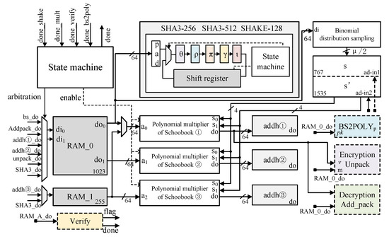
Figure 7.
Implementation for resource-constrained scenarios of Saber.
The overall circuit consists of three lightweight Schoolbook polynomial multipliers, two 64-bit-wide BRAMs ( with a depth of 1024 and with a depth of 256), a 4-bit-wide dual-port BRAM with a depth of 2048, a hash function module, three modules, and four other functional sub-modules, including . During the operation of the circuit, in the phase, the hash function module requires a 256-bit random seed as input. This seed is provided by the external user and is input into . The hash function then reads the seed from to generate an internal random seed. In the and functions, the hash function SHAKE-128 first generates pseudo-random numbers for the secret polynomials, which are stored in . It then generates coefficients for the public polynomials, which are also stored in . At the same time as generating the coefficients for the public polynomials, the binomial distribution sampling module initiates parallel operation. It requires two cycles to read data and in the write-back stage, 8 bits of data are serially shifted out per cycle. The total sampling period requires (2 + 8) × 48 + 1 = 481 cycles, which is smaller than the 687 clock cycles required for generating the coefficients of the public polynomials.
Although the lightweight Schoolbook multiplier for single polynomial multiplication does not have the additional overhead cycles mentioned in other literature, it still requires 16,384 cycles due to its low parallelism. To evaluate the entire protocol, which involves 36 polynomial multiplications, it takes approximately 590,000 cycles. Especially in the case of low-frequency implementation of the lightweight version, the delay can be relatively long. Therefore, this paper parallelizes three identical lightweight polynomial multipliers. Each multiplier performs different row-column multiplications during the matrix-vector multiplication. This reduces the number of explicit multiplications to 18, cutting the cycle count in half. The increased space for the additional multipliers is acceptable. Additionally, it is necessary to analyze the inputs and outputs of the two additional multipliers. During the generation of public polynomial coefficients, it is necessary to store the three polynomials in . This allows for the simultaneous retrieval of the three rows of public polynomials. Furthermore, since the three multipliers need to be synchronized, the reading of secret polynomials only needs to be controlled by the first multiplier. The circuit diagram shown in Figure 8 requires only one BRAM to meet the requirements of the three multipliers. This not only reduces the consumption of BRAM but also enables the remaining two multipliers to conserve logic for address generation and control signal generation during implementation. The comprehensive results show that the area consumption of the remaining two polynomial multipliers is 488 × 2 LUTs and 243 × 2 FFs. During the inner product of polynomials and vectors, certain results of matrix multiplication are stored in , requiring the retrieval of data from .
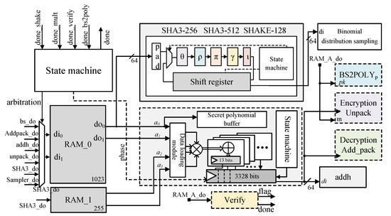
Figure 8.
High-Throughput implementation of Saber.
serves as the primary storage unit and is constantly updated to overwrite the computed data and store the recovered session key. Once the overall protocol flow is completed, the “” signal is raised. The overall performance of the Saber protocol circuit in resource-constrained scenarios will be presented later.
4.2. High-Throughput and Area-Time Balanced Implementation of Saber
An optimized Saber protocol circuit is designed specifically for the high-throughput polynomial multiplier based on TMVP-Schoolbook in Figure 8. In this circuit, the “” signal is used as an output signal, while the “” signal is used to determine whether to clear the accumulation registers within the multiplier. Only one multiplier and one module is utilized. During the multiplication operation, the circuit simultaneously reads the 4-way common polynomial coefficients from the two BRAMs. Instead of storing the data back into the BRAMs before writing it, the data are directly processed in the module. Additionally, the coefficients of the secret polynomial are read from , and the binomial distribution sampling module writes them back to . To minimize the number of cycles required for execution, it is necessary to reduce the cycle consumption in data reading and writing between modules and increase parallelism. Therefore, careful arrangement of data interaction between upstream and downstream modules is essential. The timing sequence diagrams for key generation and key encapsulation phases of the key encapsulation protocol are shown in Figure 9 and Figure 10, respectively. The key generation phase requires 2346 cycles, while the key encapsulation phase requires 3341 cycles.
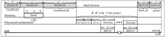
Figure 9.
Timing sequence diagram of for high-throughput implementation.
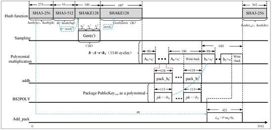
Figure 10.
Timing sequence diagram of for high-throughput implementation.
The timing arrangement for the key decapsulation process is similar to the two diagrams, requiring a total of 4005 cycles. The key decapsulation phase consumes the most cycles due to the additional operation of public key encryption. It can be observed from the timing diagrams that parallelizing the modules and minimizing idle cycles within the functional submodules significantly reduce the overall protocol execution time, thereby increasing the circuit’s throughput rate.
Additionally, the paper selects the pipelined NTT transformation structure for a better balance between speed and area. The radix-2 Multi-path Delay Commutator (MDC) NTT structure, as designed in the referenced work [18], is considered a classic approach. The architecture has no complex memory control logic and fully utilizes spare cycles in each stage, achieving high throughput. The radix-2 MDC pipelined NTT structure is employed for the Saber algorithm in this paper. The implementation and improvement of the overall NTT multiplier is illustrated in Figure 11. Based on a single MDC-NTT/INTT core, two modular multiplication units are externally added for point-wise multiplication. These modular multiplication units are similar to those in the NTT core, reducing the 45-bit value to 23-bit through modular reduction. The loading module for the public polynomial coefficients remains unchanged from the previous description. This module enables the continuous reading of 13-bit or 16-bit coefficient data streams during the forward NTT process. The “” signal selects the target of the NTT transformation. After performing NTT on one polynomial operand, the two sets of coefficients are merged and stored at the same address in the BRAM. During the NTT forward transformation of another polynomial operand, the coefficients corresponding to the previous storage in the BRAM at the respective order are read, point-wise multiplied, and accumulated when the data output starts per cycle. The input to the INTT is the result of three polynomial multiplications, followed by point-wise multiplication. The resulting polynomial is then reduced modulo the modulus or of the Saber algorithm. Finally, the sequence of results is reversed, bit by bit. The protocol circuit based on the NTT multiplier is similar to Figure 3, but with the inclusion of two 36K-bit BRAM blocks to store the data after NTT transformation and point-wise multiplication. The state machine of the entire circuit is configured to achieve module parallelism. Similarly, the timing sequence diagrams for key generation and key encapsulation are shown in Figure 12 and Figure 13, respectively. The key generation phase requires 3060 cycles, the key encapsulation phase requires 4961 cycles, and the key decapsulation phase requires 5910 cycles.
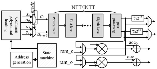
Figure 11.
NTT/INTT kernel and CWM multiplier.
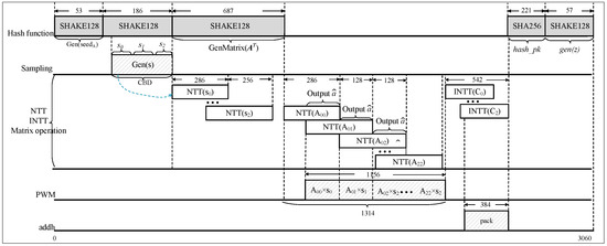
Figure 12.
Timing sequence diagram of for performance-area balance.
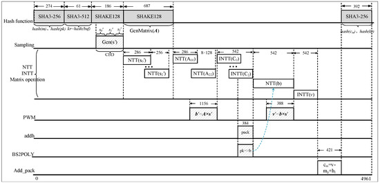
Figure 13.
Timing sequence diagram of for performance-area balance.
The main cycle optimization strategy lies in performing the NTT transformation on the secret polynomial coefficients concurrently with the generation of the public polynomial coefficients. Therefore, when the coefficients of the public polynomial undergo NTT transformation and output the first set of data, they can directly engage in point-wise multiplication with the already read from the BRAM. This way, the cycle of CWM can also be concealed through parallel operations. The protocol flow for decapsulation is similar to the previous two phases.
5. Results
Table 2 provides three hardware implementation results of the overall circuit for the Saber key encapsulation protocol, including their respective performance and resource utilization. The “” column represents the number of cycles for the key generation stage, key encapsulation stage and decapsulation stage, respectively. The “Latency” column shows the corresponding latency in seconds based on the data.
Table 2.
Implementation results of three kinds of protocol circuits for different demand scenarios and comparisons to other existing work.
This paper proposes three kinds of hardware implementation of the Saber protocol designed for resource-constrained, high-throughput and balanced scenarios. In addition to the advantages and disadvantages of their respective focus areas, in order to make a fair comparison of hardware implementations, we evaluate the actual hardware efficiency of a circuit by using a uniform index ATP (area-time product).
For the ATP index, equivalent slices (ES) refers to the logic units of an FPGA after equivalence. In the circuit design, minimizing delay and resource consumption enhances performance. Therefore, a lower ATP indicates higher hardware efficiency of the circuit and faster completion of the protocol process with fewer slices.
The current lightweight hardware implementation for resource-constrained scenarios is only available in the literature [31]. It has implemented two lightweight schemes, one of which includes side channel defense and adds mask protection. This paper compares the version without side-channel protection, which utilizes the Schoolbook algorithm with adjustable parameters for polynomial multiplication, to the overall protocol circuit structure described in this paper. However, only one multiplication module was instantiated and the storage unit was designed manually. The clock cycle decreased by 55.15% compared to the previous design. However, the equivalent slice increased by 64%, and the ATP index increased by 23.4% simultaneously. From the perspective of high performance and high throughput implementation, this implementation achieves a throughput rate of 10,988 Kbps and a TPS value of 1.5, which is the highest. This indicates that the overall protocol circuit maintains high throughput characteristics while optimizing hardware efficiency. At the same time, the ATP index is also the lowest, indicating that the circuit has achieved a good balance. The circuit architecture described in the literature [12] is a coprocessor. As mentioned above, this architecture is highly flexible and can be controlled directly by the user. It allows for the customization of specific data within the circuit to facilitate the desired process. However, compared to a dedicated circuit, it has disadvantages in terms of clock cycle delay, frequency, and overall performance. Although the equivalent slice is reduced by 58% compared to this design, the clock period is increased by 51.8% and the overall delay is increased by 71.04% compared to this design. The overall implementation of the literature [30] is very efficient. Polynomial multiplication is performed immediately when the hash function generates common polynomial coefficients. Additionally, a ping-pong buffer is used, which allows the polynomial multiplication to omit the cycle cost of this part through parallel operation. Therefore, the overall protocol process only takes 4223 cycles, which is 56.4% less than the implementation. This shows that the implementation also includes specific optimizations for the hash module, particularly in the input and output sections. However, due to the critical path problem mentioned earlier, the frequency can only reach 160 MHz, resulting in a 12.3% slower latency. The excessive DSP also resulted in a 47.1% increase in equivalent slice and a 53.3% increase in ATP value compared to this implementation. When compared with the literature [16], which also utilizes an NTT multiplier, this design exhibits a 43.9% increase in frequency, a 70.8% reduction in clock cycle and a 28.6% increase in equivalent slice consumption. But again, the disadvantage of Saber based on NTT multipliers is that the data bit width of the multiplier is larger and consumes more resources compared to other lattice cryptography schemes that are compatible with NTT.
6. Conclusions
In this paper, we propose three types of polynomial multipliers for various application scenarios including the lightweight Schoolbook multiplier, high-throughput multiplier based on the TMVP-Schoolbook algorithm and improved pipelined NTT multiplier. Moreover, other principal modules of Saber are designed, encompassing the hash function module, sampling module and functional submodule. Based on our proposed multiplier, we implement the overall hardware circuits of the Saber key encapsulation protocol. Experimental results demonstrate that our overall hardware circuits have different advantages. Our lightweight implementation has minimal resource consumption. Our high-throughput implementation needs only 23.28 s to complete the whole process, which is the fastest among the existing works. The throughput rate is 10,988 Kbps and the frequency is 416 MHz. Our hardware implementation based on the improved pipelined NTT multiplier achieved a good balance between area and performance. The overall frequency can reach 357 MHz. Regarding the actual circuit design strategy, despite Saber being eliminated by NIST, the Schoolbook multiplier proposed in this paper is independent of parameters and applicable to any lattice cipher. Further investigation into the applicability to other ciphers, particularly CRYSTALS-Kyber, is essential.
Author Contributions
Conceptualization, D.L. and Y.C.; methodology, D.L. and Y.Z.; software, Y.Z.; validation, J.Z. and Y.Z.; formal analysis, Y.Z. and S.G.; investigation, D.L., S.C. and Y.Z.; resources, S.G.; data curation, Y.Z. and S.C.; writing—original draft preparation, J.Z.; writing—review and editing, Y.C.; visualization, Y.Z.; supervision, Y.C.; project administration, Y.C.; funding acquisition, S.G. All authors have read and agreed to the published version of the manuscript.
Funding
This work is supported by the Laboratory Open Fund of Beijing Smart-Chip Microelectronics Technology Co. Ltd. under Grant SGSC0000SJQT2207160.
Data Availability Statement
Data is contained within the article.
Conflicts of Interest
Author Dejian Li, Song Cheng and Shunxian Gao was employed by the company Beijing Smart-Chip Microelectronics Technology Co. Ltd. The remaining authors declare that the research was conducted in the absence of any commercial or financial relationships that could be construed as a potential conflict of interest.
References
- Peikert, C. Public-key cryptosystems from the worst-case shortest vector problem: Extended abstract. In Proceedings of the Forty-First Annual ACM Symposium on Theory of Computing, Bethesda, MD, USA, 31 May–2 June 2009; pp. 333–342. [Google Scholar]
- Easttom, C. Lattice-Based Cryptography. Modern Cryptography: Applied Mathematics for Encryption and Information Security; Springer International Publishing: Cham, Switzerland, 2022; pp. 409–425. [Google Scholar]
- Rivest, R.L.; Shamir, A.; Adleman, L.M. A method for obtaining digital signatures and public-key cryptosystems. Commun. ACM 1978, 21, 120–126. [Google Scholar] [CrossRef]
- Targhi, E.E.; Unruh, D. Post-Quantum Security of the Fujisaki-Okamoto and OAEP Transforms. In Proceedings of the Theory of Cryptography, Beijing, China, 31 October–3 November 2016; Hirt, M., Smith, A., Eds.; Springer: Berlin/Heidelberg, Germany, 2016; pp. 192–216. [Google Scholar]
- Yesina, M.V.; Ostrianska, Y.V.; Gorbenko, I. Status report on the third round of the NIST post-quantum cryptography standardization process. In National Institute of Standards and Technology; US Department of Commerce, NIST: Gaithersburg, MD, USA, 2022. [Google Scholar]
- Zhang, J.; Zhang, Z. Lattice-Based Cryptosystems: A Design Perspective. In Lattice-Based Cryptosystems; Springer: Singapore, 2020; pp. 978–981. [Google Scholar]
- Ding, J.; Lindner, R. Identifying Ideal Lattices. Cryptol. Eprint Arch. 2007, 322. [Google Scholar]
- Kuchta, V.; Sakzad, A.; Stehlé, D. Measure-Rewind-Measure: Tighter quantum random oracle model proofs for one-way to hiding and CCA security. In Advances in Cryptology – EUROCRYPT 2020; Canteaut, A., Ishai, Y., Eds.; Springer International Publishing: Cham, Switzerland, 2020; pp. 703–728. [Google Scholar]
- Joseph, D.; Misoczki, R.; Manzano, M.; Tricot, J.; Pinuaga, F.D.; Lacombe, O.; Leichenauer, S.; Hidary, J.D.; Venables, P.; Hansen, R. Transitioning organizations to post-quantum cryptography. Nature 2022, 605, 237–243. [Google Scholar] [CrossRef] [PubMed]
- D’Anvers, J.P.; Karmakar, A.; Sinha Roy, S.; Vercauteren, F. Saber: Module-LWR Based Key Exchange, CPA-Secure Encryption and CCA-Secure KEM. In Progress in Cryptology–AFRICACRYPT 2018; Joux, A., Nitaj, A., Rachidi, T., Eds.; Springer International Publishing: Cham, Switzerland, 2018; pp. 282–305. [Google Scholar]
- Regev, O. On lattices, learning with errors, random linear codes, and cryptography. In Proceedings of the Thirty-Seventh Annual ACM Symposium on Theory of Computing, Baltimore, MD, USA, 22–24 May 2005; Volume 67, pp. 84–93. [Google Scholar]
- Roy, S.S.; Basso, A. High-speed Instruction-set Coprocessor for Lattice-based Key Encapsulation Mechanism: Saber in Hardware. IACR Trans. Cryptogr. Hardw. Embed. Syst. 2020, 2020, 443–466. [Google Scholar]
- Dworkin, M. SHA-3 Standard: Permutation-Based Hash and Extendable-Output Functions; Federal Information Processing Standards Publication, National Institute of Standards and Technology: Gaithersburg, MD, USA, 2015. [CrossRef]
- Zhu, Y.; Zhu, W.; Zhu, M.; Li, C.; Deng, C.; Chen, C.; Yin, S.; Yin, S.; Wei, S.; Liu, L. A 28nm 48KOPS 3.4µJ/Op Agile Crypto-Processor for Post-Quantum Cryptography on Multi-Mathematical Problems. In Proceedings of the 2022 IEEE International SolidState Circuits Conference (ISSCC), San Francisco, CA, USA, 20–26 February 2022; Volume 65, pp. 514–516. [Google Scholar]
- Basso, A.; Aydin, F.; Dinu, D.; Friel, J.; Varna, A.L.; Sastry, M.R.; Ghosh, S.K. Where Star Wars Meets Star Trek: SABER and Dilithium on the Same Polynomial Multiplier. IACR Cryptol. ePrint Arch. 2021, 2021, 1697. [Google Scholar]
- Aikata, A.; Mert, A.C.; Jacquemin, D.; Das, A.; Matthews, D.; Ghosh, S.K.; Roy, S.S. A Unified Cryptoprocessor for Lattice-Based Signature and Key-Exchange. IEEE Trans. Comput. 2023, 72, 1568–1580. [Google Scholar] [CrossRef]
- Dang, V.B.; Mohajerani, K.; Gaj, K. High-Speed Hardware Architectures and FPGA Benchmarking of CRYSTALS-Kyber, NTRU, and Saber. IEEE Trans. Comput. 2023, 72, 306–320. [Google Scholar] [CrossRef]
- Renteria-Mejia, C.P.; Velasco-Medina, J. High-Throughput Ring-LWE Cryptoprocessors. IEEE Trans. Very Large Scale Integr. (VLSI) Syst. 2017, 25, 2332–2345. [Google Scholar] [CrossRef]
- Renteria-Mejia, C.P.; Velasco-Medina, J. Lattice-Based Cryptoprocessor for CCA-Secure Identity-Based Encryption. IEEE Trans. Circuits Syst. I Regul. Pap. 2020, 67, 2331–2344. [Google Scholar] [CrossRef]
- He, P.; Lee, C.Y.; Xie, J. Compact Coprocessor for KEM Saber: Novel Scalable Matrix Originated Processing. In Proceedings of the NIST Third Standardization Conference, Virtually, 7–9 June 2021; pp. 1–16. [Google Scholar]
- Regev, O.; Rosen, R. Lattice problems and norm embeddings. In Proceedings of the 38th Annual ACM Symposium on Theory of Computing, Seattle, WA, USA, 21–23 May 2006; pp. 447–456. [Google Scholar]
- Goldreich, O.; Lindell, Y. Session-Key Generation Using Human Passwords Only. In Proceedings of the Advances in Cryptology— CRYPTO 2001, Santa Barbara, CA, USA, 19–23 August 2001; Kilian, J., Ed.; Springer: Berlin/Heidelberg, Germany, 2001; pp. 408–432. [Google Scholar]
- Bao, T.; He, P.; Xie, J. Systolic Acceleration of Polynomial Multiplication for KEM Saber and Binary Ring-LWE Post-Quantum Cryptography. In Proceedings of the 2022 IEEE International Symposium on Hardware Oriented Security and Trust (HOST), McLean, VA, USA, 27–30 June 2022; pp. 157–160. [Google Scholar]
- Zhang, Y.; Cui, Y.; Ni, Z.; e Shahwar Kundi, D.; Liu, D.; Liu, W. A Lightweight and Efficient Schoolbook Polynomial Multiplier for Saber. In Proceedings of the 2022 IEEE International Symposium on Circuits and Systems (ISCAS), Austin, TX, USA, 27 May–1 June 2022; pp. 2251–2255. [Google Scholar]
- Oudin, M.; Delmas, J.P. Asymptotic generalized eigenvalue distribution of Toeplitz block Toeplitz matrices. In Proceedings of the 2008 IEEE International Conference on Acoustics, Speech and Signal Processing, Las Vegas, NV, USA, 31 March–4 April 2008; pp. 3309–3312. [Google Scholar]
- Zhang, Y.; Wang, C.; e Shahwar Kundi, D.; Khalid, A.; O’Neill, M.; Liu, W. An Efficient and Parallel R-LWE Cryptoprocessor. IEEE Trans. Circuits Syst. II Express Briefs 2020, 67, 886–890. [Google Scholar] [CrossRef]
- De Jesús Angel Angel, J.; Morales-Luna, G.B. Solinas primes of small weight for fixed sizes. IACR Cryptol. ePrint Arch. 2010, 2010, 58. [Google Scholar]
- Bertoni, G.; Daemen, J.; Peeters, M.; Assche, G.V. Keccak. In Advances in Cryptology–EUROCRYPT 2013; Johansson, T., Nguyen, P.Q., Eds.; Springer: Berlin/Heidelberg, Germany, 2012; pp. 313–314. [Google Scholar]
- Tan, W.; Wang, A.; Lao, Y.; Zhang, X.; Parhi, K.K. Low-Latency VLSI Architectures for Modular Polynomial Multiplication via Fast Filtering and Applications to Lattice-Based Cryptography. In Proceedings of the 2008 IEEE International Conference on Acoustics, Speech and Signal Processing, Las Vegas, NV, USA, 31 March–4 April 2008. [Google Scholar]
- Zhu, Y.; Zhu, M.; Yang, B.; Zhu, W.; Deng, C.; Chen, C.; Wei, S.; Liu, L. LWRpro: An Energy-Efficient Configurable Crypto-Processor for Module-LWR. IEEE Trans. Circuits Syst. I Regul. Pap. 2021, 68, 1146–1159. [Google Scholar] [CrossRef]
- Abdulgadir, A.; Mohajerani, K.; Dang, V.B.; Kaps, J.P.; Gaj, K. A Lightweight Implementation of Saber Resistant Against Side-Channel Attacks. In Proceedings of the International Conference on Cryptology in India, Jaipur, India, 12–15 December 2021; pp. 224–245. [Google Scholar]
Disclaimer/Publisher’s Note: The statements, opinions and data contained in all publications are solely those of the individual author(s) and contributor(s) and not of MDPI and/or the editor(s). MDPI and/or the editor(s) disclaim responsibility for any injury to people or property resulting from any ideas, methods, instructions or products referred to in the content. |
© 2024 by the authors. Licensee MDPI, Basel, Switzerland. This article is an open access article distributed under the terms and conditions of the Creative Commons Attribution (CC BY) license (https://creativecommons.org/licenses/by/4.0/).