Article

FPGA-Accelerated Erasure Coding Encoding in Ceph Based on an Efficient Layered Strategy

1
School of Computer and Information Security, Guilin University of Electronic Technology, No. 1 Jin Ji Road, Guilin 541004, China
2
School of Computer Science and Engineering, Guilin University of Aerospace Technology, No. 2 Jin Ji Road, Guilin 541004, China
3
Guangxi Engineering Technology Research Center of Cloud Security and Cloud Service, Guilin University of Electronic Technology, No. 1 Jin Ji Road, Guilin 541004, China
*
Author to whom correspondence should be addressed.
Electronics 2024, 13(3), 593; https://doi.org/10.3390/electronics13030593
Submission received: 11 January 2024 / Revised: 29 January 2024 / Accepted: 29 January 2024 / Published: 31 January 2024

Abstract

:
Distributed storage systems such as Ceph have been widely adopted, with erasure coding technology being an essential fault-tolerance technique. While ensuring data reliability and security, it significantly reduces the cost of data storage. Due to the computational overhead and encoding latency introduced by the erasure coding process, the data encoding rate is often constrained. To address this issue, an FPGA-accelerated erasure coding encoding scheme in Ceph, based on an efficient layered strategy (FPGA-Accelerated Erasure Coding Encoding in Ceph with an Efficient Layered Strategy, LFEC-Accelerator), is proposed and implemented. This approach takes full advantage of FPGA’s parallel computing capabilities to accelerate the erasure coding algorithm at the hardware level. Furthermore, to maximize the utilization of the FPGA controller’s resources and ensure that all processing steps are properly managed and scheduled, our approach introduces a hierarchical structure comprising a communication interface layer, task scheduling layer, and hardware acceleration layer. Experimental results indicate that, under the same erasure coding configurations and file sizes, our solution outperforms native Ceph-supported erasure coding libraries such as Jerasure, Clay, Shec and ISA, with an encoding rate improvement of up to 3.04 times.

1. Introduction

In contemporary times, technological advancements have catalyzed explosive growth in domains such as the internet, cloud computing and big data. The data scale has expanded to magnitudes beyond the processing capabilities of traditional storage systems [1]. In such an environment, there is an exigent demand for novel data storage systems that demonstrate robust data handling, stability and scalability. Hence, distributed storage systems, including Hadoop’s HDFS [2], Swift cloud storage [3] and Ceph [4], have emerged and are widely adopted for data storage and management.
However, an inescapable issue these systems face is data loss, which may arise from circumstances including disk failures, filesystem crashes, extreme natural disasters and operational errors [5]. Such incidents can lead to node failures, resulting in significant data losses. To mitigate data loss risks and enhance system stability, replica redundancy techniques [6] and erasure coding [7] are commonly adopted in distributed systems. Replica redundancy improves data availability by copying data onto other nodes, whereas erasure coding divides and encodes the original data, generating parity chunks for data recovery [8].
The theory of erasure coding dates back to the 1960s, with the Reed–Solomon algorithm [9] being the most renowned. Over time, various adaptations of this algorithm have emerged, such as Fountain Codes [10], Pyramid Codes [11] and Local Repairable Codes [12]. Erasure coding typically requires defining a quantity of data chunks (m) and parity chunks (k). Under such configurations, up to k disk failures can be tolerated. For instance, in a typical Reed–Solomon scheme ( 5 , 3 ) , where 5 represents data chunks and 3 indicates parity chunks, RS ( 5 , 3 ) can withstand failures of any three disks. Should certain data chunks be lost, the original content can be recovered using the remaining available data [13].
In cloud storage, replica redundancy is conventionally employed to ensure system availability. However, when storage scales to petabytes, the required capacity becomes exorbitantly high [14]. Utilizing erasure coding can significantly reduce storage space without compromising availability, substantially reducing the Total Cost of Ownership (TCO). From the Firefly release onward, Ceph has incorporated support for erasure coding, offering several plugins, including Clay, Jerasure, LRC, Shec and ISA.
While erasure coding has been widely implemented in data centers, boasting cost-efficiency, its encoding processes can introduce computational burdens and latency [15]. Data loss during encoding can make the recovery of original data chunks impossible, adversely impacting system performance and stability. Consequently, solutions based on Field-Programmable Gate Arrays (FPGA) [16], noted for their customizable logic structures, efficient parallel computing capabilities and flexible scheduling performance, have been eyed as ideal tools for accelerating erasure coding computations.
Though FPGAs are frequently utilized to achieve low-latency forward error correction encoding/decoding in high-speed network communication [17], existing FPGA-based erasure coding acceleration solutions are primarily validated through simulation or in standalone modes [18]. In actual distributed storage systems, challenges related to communication reliability and handling large data blocks persist. To address this, we introduce an FPGA-accelerated erasure coding scheme for the distributed storage system, Ceph, based on an efficient hierarchical strategy seeking to diminish the latency of erasure coding and enhance the stability of erasure-coded fault-tolerant storage. We experimentally validate this approach in a real distributed storage setting.
Our primary contributions in this work are:
Design and Implementation of LFEC-Accelerator: We have crafted and executed an FPGA-accelerated erasure coding scheme named LFEC-Accelerator for distributed storage environments. Harnessing the parallel computation potential of FPGAs, it achieves erasure coding computations at the hardware level efficiently.
Deep Integration of LFEC-Accelerator with Ceph: We have integrated the LFEC-Accelerator profoundly within the Ceph distributed storage system. By designing specific communication interfaces and task scheduling mechanisms, we ensure efficient collaboration between the LFEC-Accelerator and Ceph.
Performance Evaluation of LFEC-Accelerator: We have conducted a comprehensive performance assessment of the LFEC-Accelerator and contrasted it with native Ceph-supported erasure coding plugins. According to our evaluations, the LFEC-Accelerator considerably outperforms the native plugins, with an encoding rate enhancement of up to 3.04 times, attesting to its superiority.
The structure of this paper is as follows: Section 2 delves deeply into the foundational principles of erasure coding and relevant studies on encoding optimization. Section 3 elaborates on the hierarchical design and implementation of the LFEC-Accelerator, covering communication interface layers, task scheduling layers, data transmission modules in hardware acceleration layers and erasure encoders. Furthermore, this section also delineates the deep integration of the LFEC-Accelerator with Ceph. Section 4 thoroughly evaluates the performance of the LFEC-Accelerator. Finally, Section 5 concludes the paper and looks forward to future research directions.

2. Background and Related Work

In this section, we delve into the background and related work that forms the foundation of our study. Initially, we introduce the fundamentals of Erasure Coding, a pivotal technology in achieving fault tolerance through redundant coding. This section not only outlines the basic principles of Erasure Coding but also explores its critical role in distributed storage systems. We then provide a detailed analysis of the existing literature, highlighting the advancements in the field and identifying gaps that our research aims to address. By examining the evolution of Erasure Coding and its optimization in various applications, we set the stage for our contribution to this domain. The subsequent subsections will comprehensively cover the encoding and decoding processes, their mathematical underpinnings and the challenges encountered in their practical implementation. Through this, we aim to offer a thorough understanding of the current state of Erasure Coding and its significance in modern data storage solutions.

2.1. Fundamentals of Erasure Coding

Erasure coding technology is a fault-tolerance strategy based on redundant coding, aiming to create independently stored original data blocks and redundant data blocks. Its key function is to enable effective recovery using the remaining data when some data are lost. During its implementation, a specific encoding matrix is utilized to generate m check blocks from k original data blocks. These data blocks and check blocks (with a total count of n = k + m ) are stored across various nodes in a distributed system. In cases of node failures or similar events, data recovery can be performed by reading any k blocks from the remaining ones. The system can withstand the simultaneous loss of up to m data blocks or check blocks. In this process, the procedure of generating check data is referred to as encoding, while the recovery process following data loss is termed decoding. Compared to multiple replication techniques, erasure coding boasts lower redundancy and higher disk utilization, achieving higher reliability with relatively lower storage overhead. There are various types of erasure codes, including Reed–Solomon (RS) type erasure codes, cascaded low-density erasure codes and digital fountain codes, among others [19]. Of these, RS codes have been extensively used in various storage systems. This section will further use RS code as an example to elaborate on the encoding and decoding processes.

2.1.1. Encoding Process

For RS code ( k , m ) , the parameter k represents the number of original data blocks, and m indicates the number of check blocks. Let d i represent the ith original data block ( 0 i < k ) , c j represent the jth generated check block ( 0 j < m ) , and E n signify the nth encoding block (a collection of both original data blocks and check blocks, 0 n < k + m ). To simplify computations, the erasure coding and decoding process generally take place within a Galois finite field of specified bit width. Within the finite field GF ( 2 w ) of bit width w, the encoding process is equivalent to a matrix dot multiplication operation, as illustrated by Equation (1).
E = M e n c o d e × D
where M encode represents the encoding matrix, composed of the identity matrix I and the generation matrix G, i.e., M encode = [ I | G ] T ; D represents the original data blocks, i.e., D = [ d 0 d 1 d k 1 ] T ; E represents the encoded data blocks, consisting of the original data blocks D and check data blocks, i.e., E = [ D | C ] T ; taking RS(8,4) as an example, its encoding process is shown in Equation (2).
d 0 d 1 d 2 d 3 d 4 d 5 d 6 d 7 c 0 c 1 c 2 c 3 = 1 0 0 0 0 0 0 0 0 1 0 0 0 0 0 0 0 0 1 0 0 0 0 0 0 0 0 1 0 0 0 0 0 0 0 0 1 0 0 0 0 0 0 0 0 1 0 0 0 0 0 0 0 0 1 0 0 0 0 0 0 0 0 1 m 0 , 0 m 0 , 1 m 0 , 2 m 0 , 3 m 0 , 4 m 0 , 5 m 0 , 6 m 0 , 7 m 1 , 0 m 1 , 1 m 1 , 2 m 1 , 3 m 1 , 4 m 1 , 5 m 1 , 6 m 1 , 7 m 2 , 0 m 2 , 1 m 2 , 2 m 2 , 3 m 2 , 4 m 2 , 5 m 2 , 6 m 2 , 7 m 3 , 0 m 3 , 1 m 3 , 2 m 3 , 3 m 3 , 4 m 3 , 5 m 3 , 6 m 3 , 7 m 4 , 0 m 4 , 1 m 4 , 2 m 4 , 3 m 4 , 4 m 4 , 5 m 4 , 6 m 4 , 7 m 5 , 0 m 5 , 1 m 5 , 2 m 5 , 3 m 5 , 4 m 5 , 5 m 5 , 6 m 5 , 7 m 6 , 0 m 6 , 1 m 6 , 2 m 6 , 3 m 6 , 4 m 6 , 5 m 6 , 6 m 6 , 7 m 7 , 0 m 7 , 1 m 7 , 2 m 7 , 3 m 7 , 4 m 7 , 5 m 7 , 6 m 7 , 7 d 0 d 1 d 2 d 3 d 4 d 5 d 6 d 7
In general, the generation matrix G in RS erasure coding is composed of the Vandermonde matrix or the Cauchy matrix. An α × β order Vandermonde matrix is formed by the powers from 0 to α 1 of the β elements g 0 , g 1 , , g β 1 from a specific finite field, as expressed in Equation (3).
V a n d e r m o n d e matrix = 1 1 1 1 1 g 0 g 1 g 2 g β 2 g β 1 g 0 α 1 g 1 α 1 g 2 α 1 g β 2 α 1 g β 1 α 1
The α × β order Cauchy matrix is constructed from two sets of distinct elements g 0 , g 1 , , g α 1 and f 0 , f 1 , , f β 1 from a specific finite field through the operation ( g i + f j ) 1 (where 0 i < α and 0 j < β ). This is expressed as Equation (4).
C a u c h y matrix = 1 g 0 + f 0 1 g 0 + f 1 1 g 0 + f 2 1 g 0 + f β 2 1 g 0 + f β 1 1 g 1 + f 0 1 g 1 + f 1 1 g 1 + f 2 1 g 1 + f β 2 1 g 1 + f β 1 1 g α 1 + f 0 1 g α 1 + f 1 1 g α 1 + f 2 1 g α 1 + f β 2 1 g α 1 + f β 1

2.1.2. Decoding Process

When some data blocks or check blocks are damaged, the process of restoring the damaged data blocks is completed by performing the same dot multiplication operation as the encoding process with the remaining surviving blocks and the decoding matrix. This process is called decoding. To restore the damaged data blocks E erasure , one needs to determine the decoding matrix M decode , and then by performing matrix dot multiplication with the surviving data blocks E survived in the finite field, the damaged data blocks E erasure can be restored, as expressed in Equation (5).
E e r a s u r e = M d e c o d e × E s u r v i v e d
The crux of the decoding problem lies in determining the decoding matrix M decode . Let us elucidate the solution process using the aforementioned RS(8,4) as an example. Assume the data blocks d 1 , d 5 and the check blocks c 1 , c 2 are lost (i.e., E erasure = [ d 1 d 5 c 1 c 2 ] T ). Here, we define the encoding matrix corresponding to the damaged data or check blocks as the erasure matrix M erasure . This is expressed in Equation (6).
M matrix = 0 1 0 0 0 0 0 0 0 0 0 0 0 1 0 0 m 1 , 0 m 1 , 1 m 1 , 2 m 1 , 3 m 1 , 4 m 1 , 5 m 1 , 6 m 1 , 7 m 2 , 0 m 2 , 1 m 2 , 2 m 2 , 3 m 2 , 4 m 2 , 5 m 2 , 6 m 2 , 7
Similarly, the surviving data and check blocks E survived = [ d 0 d 2 d 3 d 4 d 6 d 7 c 0 c 3 ] T are associated with an encoding matrix termed the survival matrix M survived , as shown in Equation (7).
M survived = 1 0 0 0 0 0 0 0 0 0 1 0 0 0 0 0 0 0 0 1 0 0 0 0 0 0 0 0 1 0 0 0 0 0 0 0 0 0 1 0 0 0 0 0 0 0 0 1 m 0 , 0 m 0 , 1 m 0 , 2 m 0 , 3 m 0 , 4 m 0 , 5 m 0 , 6 m 0 , 7 m 3 , 0 m 3 , 1 m 3 , 2 m 3 , 3 m 3 , 4 m 3 , 5 m 3 , 6 m 3 , 7
From the encoding process, it is known that the surviving data blocks are the result of multiplying the survival matrix with the encoded data block E, and the damaged data blocks result from multiplying the erasure matrix with the encoded data block E, as in Equation (8).
E survived = M survived × E , E erasure = M erasure × E .
Regardless of whether the generation matrix is a Vandermonde matrix or a Cauchy matrix, M erasure 1 does exist. Thus, multiplying both sides of the equation by M survived 1 yields Equation (9).
M survived 1 × E survived = M survived 1 × M survived × E , E = M survived 1 × E survived .
Substituting into Equation (8) results in Equation (10).
E e r a s u r e = M e r a s u r e × M survived 1 × E survived
Combining these, we obtain Equation (11).
M d e c o d e = M e r a s u r e × M survived 1
Substituting into Equation (5), we can then determine the damaged data block D erasure .

2.2. Research on Erasure Coding Optimization

In distributed storage systems, the application of erasure coding has been extensively researched and practiced. However, issues such as the consumption of network resources and computational efficiency remain significant challenges affecting its performance [20]. With the gradual introduction of high-performance networks such as InfiniBand [21] and RDMA [22] in storage systems, the network problems associated with data encoding have been increasingly addressed. Consequently, the efficiency of erasure coding becomes the critical factor constraining data storage recovery [23]. In the process of erasure coding, the main computational workload originates from numerous matrix dot multiplications in the Galois finite field, especially the matrix inversion during the decoding process, which becomes the primary bottleneck affecting the performance of distributed cluster erasure coding. To enhance computational speed, there have been efforts to speed up the erasure coding process by optimizing computational steps and generating matrices. For example, Kalcher et al. [24] simplified multiplications in the Galois finite field through lookup tables, further improving computational efficiency. Sun et al. [25] optimized the HRC code algorithm and introduced the HRC offset repeat code, which, compared to the triple replication technique and S2-RAID erasure code, enhanced fault tolerance and reduced repair overhead.
From a hardware architecture perspective, recent works have proposed using CPUs, GPUs and FPGAs to optimize and accelerate erasure coding. These CPU, GPU and FPGA-based schemes have made significant contributions to the improvement of storage system performance and increased data throughput. To more comprehensively showcase these CPU, GPU, and FPGA-based solutions and their contributions to enhancing storage system performance and data throughput, Table 1 summarizes the recent relevant research works. This table details the hardware types used in each study, the testing environments, the features of the distributed technology and the main gains achieved through these technologies, thus offering readers a quick reference to understand the practical applications and effects of these techniques.
CPU-based erasure coding acceleration solutions: Currently, SIMD technology based on CPUs is commonly used for the parallel processing of data, enabling simultaneous operations on multiple data units, significantly improving the throughput of erasure coding [26]. Additionally, Chen et al. have exploited the task parallelism of multi-core CPUs and successfully implemented a parallel computing erasure coding software named parEC, addressing the bottleneck faced by single-process erasure coding [27].
GPU-based erasure coding acceleration solutions: Erasure coding involves a substantial amount of matrix multiplication computations, making GPU acceleration particularly apt. Compared to the Jerasure Version 1.2 erasure coding library, Curry et al. [28] introduced a GPU-implemented RS erasure coding library named Gibraltar, offering higher throughput and almost equivalent encoding and decoding performance. Liu et al. [29] also harnessed the vector operations and parallel processing advantages of GPUs to speed up erasure coding encoding/decoding computations. Zhao et al. [30] implemented a system prototype named Gest using GPU encoding, demonstrating high data availability, space efficiency and I/O performance in various test environments.
FPGA-based erasure coding acceleration solutions: FPGAs are favored for erasure coding acceleration due to their abundant on-chip logic, capability to achieve high throughput through pipelining parallel methods, and relatively low memory access bandwidth requirements. Xilinx [31] provides a decoding acceleration solution that adopts the idea of matrix preprocessing, eliminating the complex matrix inversion process during decoding. It stores the decoding matrix directly in the FPGA’s on-chip ROM and offers an efficient lookup table algorithm, significantly enhancing decoding throughput. Wang [32] followed this idea, using the Xilinx HLS tool to implement encoding and decoding acceleration for four types of RS codes. By designing an FPGA-based multi-rate RS encoder-decoder and adopting the matrix preprocessing concept, the constructed matrix-related delays during erasure coding were minimized. Simulations confirmed its computational capabilities and efficiency, indicating a noticeable enhancement in data throughput. Chen et al. [33] introduced an OpenCL-based erasure coding solution, which divided the original data chunks requiring verification computations into multiple matrix blocks for parallel processing. They compared acceleration architectures (GPU, APU, FPGA, MC-CPU and ST-CPU), and the results showed that FPGAs are suitable for accelerating erasure coding computations, boasting high throughput and cost-efficiency.

3. Design and Implementation of LFEC-Accelerator

To enhance the performance of the Ceph distributed storage system based on an erasure coding fault-tolerance mechanism, this paper introduces an FPGA-accelerated erasure coding scheme based on a hierarchical strategy. Firstly, we designed and implemented an FPGA controller named LFEC-Accelerator. This controller includes modular FPGA design and erasure coding encoders, capable of performing efficient erasure coding calculations at the hardware level. Through parallel processing and timing optimization, it fully leverages the parallel computing capabilities of FPGA, significantly improving data throughput. Subsequently, the LFEC-Accelerator was deeply integrated into the Ceph system, designing specialized communication interface layers, task scheduling layers and hardware acceleration layers to achieve efficient erasure coding in a distributed environment. The LFEC-Accelerator acts as a node in the Ceph cluster, responsible for receiving files to be processed, then uses FPGA for erasure coding, and returns the encoded results to the Ceph cluster.

3.1. LFEC-Accelerator Architecture Design

LFEC-Accelerator, as the core component designed in this paper, consists of a host connected to the Ceph cluster and a high-performance FPGA. The design of this structure aims to achieve efficient erasure coding in a distributed environment.
Figure 1 shows the internal structure of LFEC-Accelerator. In this figure, one can clearly see the connection between the host and the FPGA via a 10G optical network. The host is the brain of the entire system, responsible for processing and preparing data for FPGA to perform erasure coding calculations. We will detail the process of LFEC-Accelerator handling files.
When the host receives a file, it immediately starts a conversion process, converting the file content into a hexadecimal format. This conversion ensures the integrity and accuracy of the data in subsequent processing. Then, the host divides the data blocks. This is a crucial step as it determines how data are allocated to the FPGA for encoding. Additionally, the host sets encoding parameters, which determine how erasure coding is performed, such as deciding which erasure coding algorithm to use and selecting the appropriate coding rate.
To speed up data transmission to FPGA, the LFEC-Accelerator uses a 10-gb optical interface. This high-speed interface ensures that data can be quickly transferred from the host to the FPGA. However, a high-speed interface alone is not enough. To further improve transmission efficiency, we also integrated socket programming techniques. By employing multi-processes and process pools, we ensured that data could be swiftly and efficiently sent to FPGA for processing.
Figure 2 describes the entire data flow process in detail. After receiving a file from the user front end, the data are first sent to the host for processing. At this stage, the file is converted into a hexadecimal format, such as using the RS(4,2) encoding format. This means that a file, after FPGA encoding, will be divided into four data blocks and two parity blocks. These four data blocks (k1_hex_file, k2_hex_file, k3_hex_file, k4_hex_file) are distributed through Ceph’s single-replica strategy, while the two parity blocks, named “m1_hex_file” and “m2_hex_file”, are stored on the LFEC-Accelerator’s host for subsequent decoding operations.
During the entire encoding process, the collaborative work between LFEC-Accelerator’s host and FPGA is crucial. The host is responsible for data preprocessing and parameter setting, while the FPGA performs the actual erasure coding. This division of labor ensures the efficient operation of the entire system, making the LFEC-Accelerator adaptable to various application scenarios. The design of the LFEC-Accelerator takes into account the erasure coding needs in a distributed environment and combines the advantages of both host and FPGA, providing users with an efficient and reliable solution.

3.2. Design and Implementation of the Communication Interface Layer

In modern distributed storage systems, efficient, accurate and secure data transmission has become an indispensable requirement. To meet this challenge, we designed a communication interface layer that serves as a bridge between the LFEC-Accelerator and the Ceph cluster. The presence of this layer ensures that all communications with the Ceph cluster are properly handled, whether it is receiving files to be processed, sending processed results, or any other necessary communication requirements. We will now delve into the design rationale and details of the communication layer.
On the LFEC-Accelerator host, a dedicated listening program was deployed. Its core function is to receive and process files from the client in real time. To ensure data integrity and the subsequent FPGA erasure coding encoding processing requirements, once a file is received, it is immediately saved, providing a data basis for subsequent processing.
Figure 3 shows the file reception flowchart for LFEC-Accelerator. This process describes how the LFEC-Accelerator receives and handles files. The process begins with the initialization of the Flask application, followed by the definition of the file reception route. When a file arrives, the system checks whether there is a file in the request, retrieves it, saves it locally, and then sends it to the FPGA for processing. Finally, the system returns a message indicating that the file has been successfully received.
In summary, the communication interface layer designed in this section thoroughly considers the data exchange requirements between the LFEC-Accelerator and the Ceph cluster. This integrated strategy not only enhances data processing and storage efficiency but also lays a solid foundation for future expansions and optimizations.

3.3. Design and Implementation of the Task Scheduling Layer

The task scheduling layer plays a crucial role in the entire system, ensuring every task is effectively allocated to appropriate hardware resources for processing. In FPGA controllers, given the limited hardware resources, the choice and implementation strategy for task scheduling are pivotal for overall performance enhancement. In traditional CPU processing systems, task scheduling is usually conducted by the operating system’s scheduler, deciding the task execution order based on task priority, resource requirements, etc. However, on hardware acceleration platforms like FPGA, task scheduling strategies need to be more precise and efficient. Given the FPGA’s strong parallel processing ability but limited resources, how to use these resources rationally, avoid resource wastage and ensure tasks are processed promptly are the main challenges faced when designing the task scheduling layer.
In FPGA controllers, the design goal of the task scheduling layer is to ensure every task is processed orderly and efficiently. To achieve this, we adopted a strategy that combines queue management with priority scheduling. We will introduce a mathematical model to describe and optimize the task scheduling process.
In detail, the task queue serves as a central storage area holding all tasks awaiting processing. Whenever a new task arrives, it is added to this queue. When the FPGA controller is not encoding, tasks in the queue are processed in the order they arrived following the First In First Out (FIFO) principle. Suppose the task queue is Q, where Q[i] represents the i-th task, then the task execution order is Q[1], Q[2], …, Q[n]. To ensure key tasks obtain timely responses, we assigned a priority to each task. When a new task is passed from the communication layer, it carries a priority tag. In the queue, tasks with higher priority have the right to cut in line, while tasks with lower priority are processed in the order they arrived.
Furthermore, to ensure that the FPGA controller is not interrupted by other tasks during the execution of encoding tasks, an execution mechanism has been designed in this paper. Once the FPGA starts executing a task, all other tasks, regardless of their priority, must wait until the current task is completed. Let E ( t ) represent the execution status of task t, where E ( t ) = 1 indicates that the task is in progress, and E ( t ) = 0 denotes the task is either uninitiated or completed. At any given moment, for all tasks, E ( t ) 1 . This is illustrated in Figure 4, which depicts the task scheduling flowchart.
The task scheduling layer is closely integrated with the communication interface layer. When the communication interface layer receives a new task request, it passes the task information to the task scheduling layer. The scheduling layer, based on current resource situations and scheduling strategies, determines the task processing method and time and then allocates the task to hardware resources in the FPGA controller for processing.
Through the aforementioned strategies and mathematical model, the task scheduling layer provides the LFEC-Accelerator with an orderly, efficient task processing environment. This simplifies task management, ensures timely task processing and also meets the real-time requirements of the entire system.

3.4. Design and Implementation of the Hardware Acceleration Layer

In this section, we delve deep into the hardware acceleration layer. This layer serves as the heart of the FPGA accelerator, encompassing the high-performance data transfer module and the erasure coding accelerator.

3.4.1. Design and Implementation of Data Transfer Module

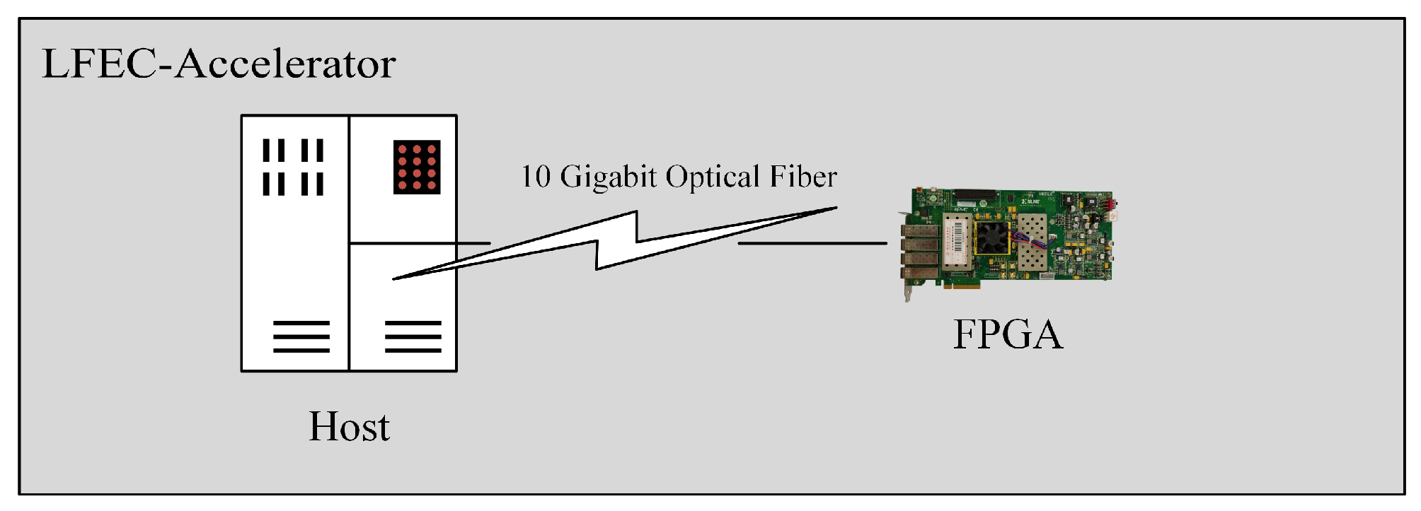
Modular design plays a pivotal role in achieving high-performance FPGA designs. Such an approach not only enhances design reusability and maintainability but also simplifies the design process, thereby boosting design efficiency. Our work leverages the Ethernet and 10G optical communication modules to establish a high-performance data transfer system.
Figure 5 shows the connection between the XPAK optical module core and the XAUI (10G Attachment Unit Interface) core. In the diagram, the 10G Ethernet MAC core handles the MAC layer of the Ethernet frame, including sending and receiving frames and frame validation. The XAUI core deals with the physical layer interface of the 10G Ethernet, including encoding and decoding of signals and link establishment and maintenance. The XPAK optical module converts electrical signals to optical signals for transmission in fiber-optic networks. Specifically, when the 10G Ethernet MAC core wishes to send an Ethernet frame, it sends the data and control information of the frame to the XAUI core. The XAUI core encodes this information into 10G Ethernet physical layer signals and passes it to the XPAK optical module via the XGMII interface. The XPAK optical module then converts these electrical signals to optical signals and transmits them via the fiber-optic network. On the receiving end, when the XPAK optical module receives optical signals it converts them to electrical signals and sends them to the XAUI core via the XGMII interface. The XAUI core then decodes these signals back to Ethernet frame data and control information and sends them to the 10G Ethernet MAC core. The 10G Ethernet MAC core then processes this information, completing the frame reception. Hence, the 10G Ethernet MAC core, XAUI core and XPAK optical module work together to transmit and receive Ethernet frames and to convert between electrical and optical signals.
In 
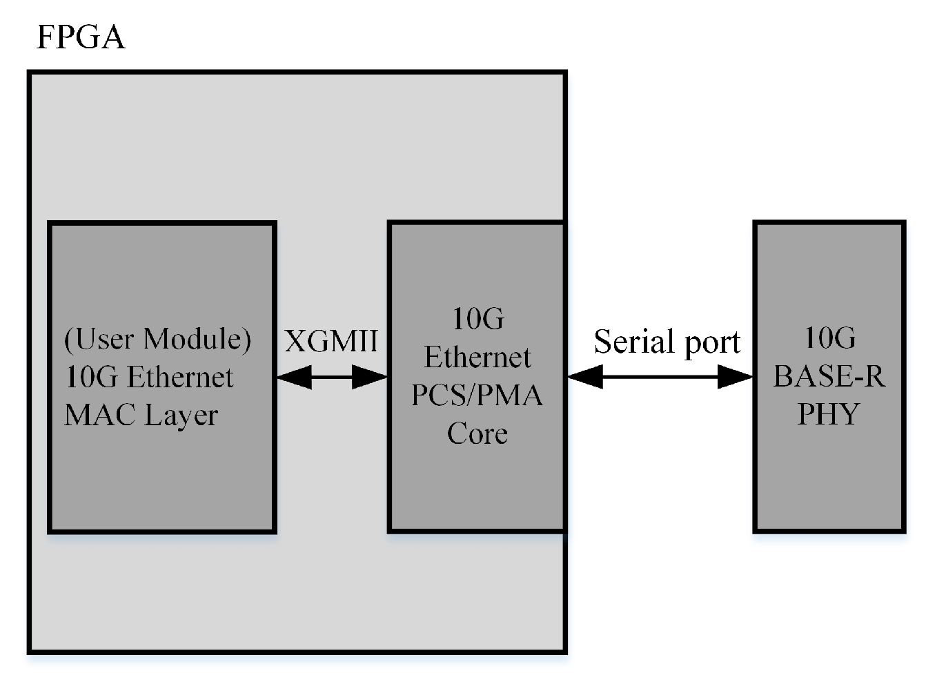
Figure 6, we see the situation when the 10G Ethernet MAC core is connected to the 10G Ethernet PCS/PMA core. In this figure, we observe the FPGA’s user logic and serial interface. The user module is part of the FPGA and can be programmed for specific tasks like data or signal processing. The serial interface is used for communications with external devices, such as network devices or other FPGAs.
In Figure 6, the connection between the user logic and serial interface is through the 10G Ethernet MAC core. This core is a hardware module designed for 10G Ethernet communication. It handles the transmission and reception of data and other Ethernet-related tasks. The figure also shows a 10G BASE-R PHY (developed for fiber optic medium). This device is responsible for the physical layer communication, converting electrical signals into optical signals for transmission in fiber-optic networks. In this system, the 10G BASE-R PHY connects to the FPGA’s serial interface, converting electrical signals from the FPGA into optical signals and vice versa. These signals are then sent to the user logic through the 10G Ethernet MAC core. Overall, Figure 6 describes a system using FPGA, a 10G Ethernet MAC core and 10G BASE-R PHY for 10G Ethernet communication, where the 10G Ethernet MAC core is central, communicating with the other components for data transmission and reception. Next, the details of data reception and transmission will be elaborated upon.
Before the FPGA receives data from the Physical Layer (PHY), several configurations and preparations are required. The FPGA needs to configure its hardware interfaces, such as the XGMII (10G Media Independent Interface), to communicate with the PHY. This involves setting the mode, speed and electrical characteristics of the interface. The XGMII interface is used to connect to the physical layer, be it a standalone device or an Ethernet MAC core implemented alongside the FPGA. Depending on design requirements, the PHY interface can be a 32-bit DDR XGMII or a 32/64-bit SDR interface, depending on the core customization. The ports of the 32-bit XGMII interface are described in Table 2.
Next, the FPGA needs to set the address of the register to be read. This is typically achieved by sending a specific address read request to the MD (Management Data Input/Output) IO interface. The read request usually contains an opcode (e.g., OP = 10 for a specific address read request), a port address (PRTAD) and a device address (DEVAD). The port and device addresses specify the location of the register in the PHY device to be read. As shown in Figure 7.
After setting the register address, the FPGA needs to send a read command to start reading the data. The read command typically contains an opcode (e.g., OP = 11 for the read command) and a Transfer Access (TA) signal. The TA signal indicates that the control of the MDIO line has shifted from the FPGA to the PHY device, which starts returning the register data.
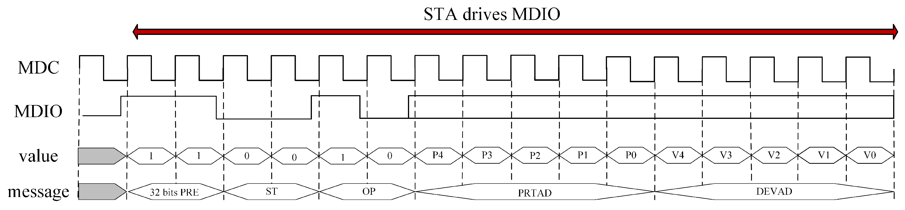
When data are input to the FPGA, a typical read process can refer to Figure 8. First, the start signal (STA) drives the Management Data Input/Output (MDIO) line, initiating the read transaction. This operation is defined by the opcode OP = 11, indicating a read transaction. Then, the port address (PRTAD) and device address (DEVAD) fields specify the location of the register to be read in the PHY device. The values of these two fields are usually set by the higher-level application or hardware logic to locate the correct data source. Following this, the Transfer Access (TA) phase begins, indicating that the control of the MDIO line has shifted from the start signal (STA) to the Media Dependent Interface (MMD). This is the phase where the data are actually read. The PHY device returns a 16-bit word from the specified register location. Finally, when the data reading is complete, the MDIO line enters the IDLE state, indicating that the current read transaction has ended and the MDIO line is free for the next transaction.
During the data transmission process, the sending device (e.g., processor or DMA controller) can send data streams to the receiving device (e.g., peripheral or memory) through the AXI4-Stream interface. AXI4-Stream (Advanced eXtensible Interface 4-Stream) is an interface protocol defined by ARM, part of the AXI4 interface specification, specifically designed for data stream communications. It supports high-performance, high-bandwidth data stream transfers and allows for continuous, non-blocking transmissions, making it suitable for applications handling large amounts of data. In the data transmission system designed in this paper, the AXI4-Stream interface is used to connect the MAC core and FIFO interface to implement data transmission. When the MAC core needs to send data, it sends the data to the FIFO interface through the AXI4-Stream interface, which then transmits the data to the physical layer.
During the data transmission process, the first thing to understand is that the data transmission interface tx_axis_tdata is logically divided into multiple channels. For a 32-bit interface, there are channels 0 to 3 and for a 64-bit interface, there are channels 0 to 7. Each channel corresponds to a tx_axis_tkeep bit which indicates whether the data on tx_axis_tdata are valid.
During the data frame transmission, the tx_axis_tvalid signal must first be set to valid, indicating that data need to be sent. At the same time, the content of the data frame should be placed on the tx_axis_tdata interface. Specifically, for a 32-bit interface, the data frame content will be divided into four parts, each 8 bits, placed on four channels. For a 64-bit interface, the content will be divided into eight parts, each 8 bits, placed on eight channels.
During the data frame transmission, the tx_axis_tlast signal will be set to valid when the last byte of each data frame is sent, indicating that the current data frame has been completely transmitted. At the same time, the tx_axis_tready signal will be set to valid once the data frame has been successfully transmitted, indicating that the interface is ready to send the next data frame.
During the data frame transmission, the tx_axis_tuser signal can also be used to indicate whether an underflow error has occurred. If the tx_axis_tuser signal is set to 0, it indicates an underflow error, and the data frame needs to be resent. If the tx_axis_tuser signal is set to 1, it indicates that the data frame has been successfully sent. Figure 9 describes the transmission process for a 32-bit frame.

3.4.2. Design and Implementation of the Reed–Solomon Encoder

Reed–Solomon encoding, as a crucial error-correcting code in digital communication and storage systems, aims to ensure the integrity and accuracy of data. The process involves taking k information symbols and producing m parity symbols, forming a complete codeword of k + m symbols. These symbols can be viewed as coefficients of a polynomial. If the entire codeword cannot be evenly divided by a certain generating polynomial, it indicates the presence of errors in the codeword. This principle is further detailed in Equation (12). The figure below presents a standard Reed–Solomon codeword format, which includes both the arrangement of information and parity symbols and the verification process using the generating polynomial.
d ( x ) = d 0 x k 1 + d 1 x k 2 + + d k 2 x 1 + d k 1 x 0 c ( x ) = x m d ( x ) = d 0 x m + k 1 + + d k 1 x m + c h e c k ( x )
An essential step in designing a Reed–Solomon encoder is the selection of an appropriate generating polynomial. This article provides recommended default generating polynomials for various symbol widths. For example, for a 4-bit symbol width, the suggested polynomial is x 4 + x + 1 . These recommended polynomials, along with their details, are tabulated in Table 3, showcasing the default generating polynomials for different symbol widths and their decimal representation.
Having chosen the generating polynomial, the next step is to determine the lengths of information and parity symbols and configure the encoder’s input and output interfaces. The setting of these interfaces requires a clear definition of key parameters such as data and control signal bit widths, clock frequency and others. The figure below gives a schematic representation of the core interfaces and signals of the encoder, as well as their interactions.
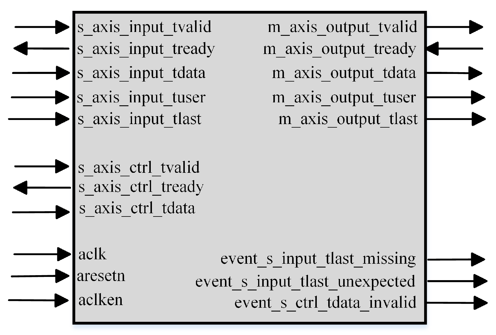
In Figure 10, the primary input and output ports of the encoder can be observed, illustrating how they interact with external devices. s_axis_input: This serves as the primary data input interface for the encoder, accepting raw data to be encoded. s_axis_ctrl: This is a control interface responsible for transmitting control signals related to the encoding process. m_axis_output: This is the encoder’s primary data output interface, where encoded data are outputted. m_axis_stat: This is a status output interface conveying status information about the encoding process. Error detection and calculation: this section denotes the core functionality of the encoder, specifically error detection and the calculation of check symbols.
Moreover, signals related to the AXI-Stream interface, such as tvalid and tready, are depicted in the figure. These signals are utilized for synchronizing data transfer and flow control. Upon data input to the Reed–Solomon encoder, the encoder first receives it via the s_axis_input interface. These data are treated as information symbols and are directed to the core section of the encoder for processing. Here, check symbols are generated based on the principles of Reed–Solomon encoding. These check symbols, combined with the original information symbols, formulate a complete Reed–Solomon codeword. Once encoding is complete, the full codeword is outputted via the m_axis_output interface. Throughout the encoding process, the encoder also detects any potential errors in the input data. If errors are detected, related status information is transmitted via the m_axis_stat interface.
To ensure efficient encoding, the encoder’s design supports multi-channel operations, allowing the encoder to process multiple data streams in parallel, significantly enhancing data processing throughput. The specific implementation of this parallel operation can be found in Figure 11. This figure provides a detailed description of the workflow in multi-channel operations, showing how data are processed in parallel across multiple channels and the direction and processing method of the data flow on each channel.
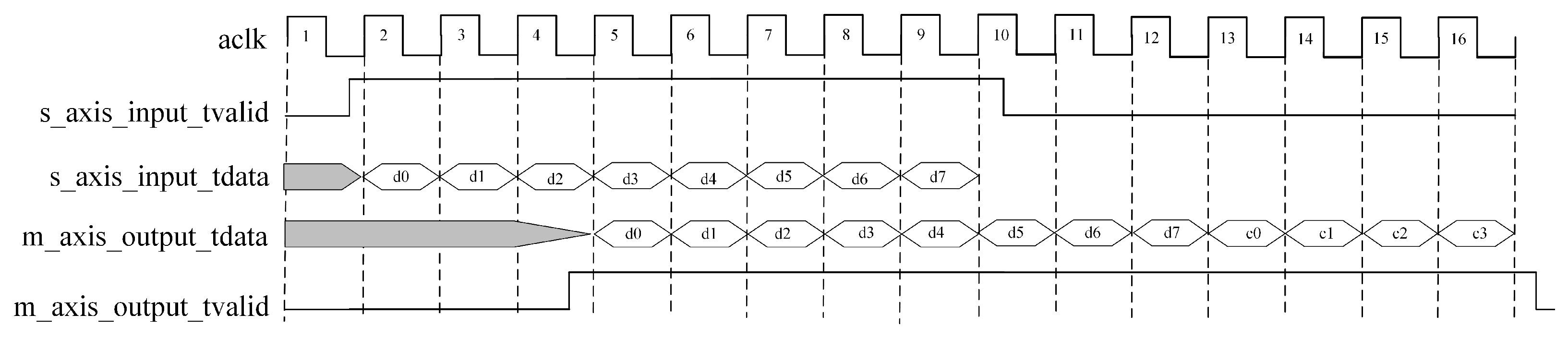
Figure 11 illustrates the multi-channel operation mode of the Reed–Solomon encoder. From the figure, it is evident how the encoder processes data from different channels in various clock cycles, realizing multi-channel parallel operations. Firstly, aclk serves as the clock signal in the figure, providing a synchronization reference for the entire operation. s_axis_input_tvalid is a validity signal; when high, it indicates that the data in s_axis_input_tdata are valid. Meanwhile, s_axis_input_tdata is the input data signal. In the figure, data blocks d0–d7 are input during clock cycles 2–9. On the output side, m_axis_output_tdata is the output data signal, and data blocks d0–d7 along with check blocks c0–c3 are input during clock cycles 5–16. Simultaneously, m_axis_output_tvalid serves as the validity signal for the output data; when high, it indicates that the data in m_axis_output_tdata have been correctly encoded and are ready for output.
Regarding data transmission, this article opts for the AXI4-Stream channel as the primary data transfer protocol. This protocol ensures data continuity and enhances data transfer efficiency. The specific data transmission process and the working method of this channel are detailed in 
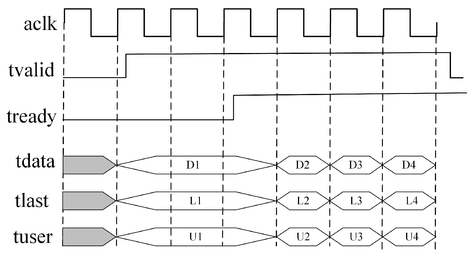
Figure 12, which presents the data transmission flow in the AXI4-Stream channel, encompassing data input, processing and output procedures, along with related control signals.
Figure 12 illustrates the data transfer process within the AXI4-Stream channel involving multiple crucial signals. First is aclk, a clock signal used for synchronizing data transfer. tvalid is driven by the source (master device), indicating the values within the payload fields (tdata, tuser and tlast) are valid. In contrast tready, driven by the receiver (slave device), signals that the slave device is prepared to receive data. tdata is the data signal transmitting the data. In the figure, it is divided into four parts representing D1, D2, D3 and D4. tlast marks the last byte of a data frame, indicating the completion of the current data frame transmission. tuser can be used to indicate specific control information or states, such as U1, U2, U3 and U4. In the AXI4-Stream channel’s data transfer process, the coordinated operation of tvalid and tready signals facilitates self-adjusting flow control. Data transfer occurs when both tvalid and tready are true. If the downstream data path is not prepared to handle the data, data loss is prevented through the back-pressure mechanism via tready. Moreover, the article also references two input channels: S_AXIS_INPUT and S_AXIS_CTRL. If block parameters configurable at runtime, such as block length, are selected, these channels are utilized. Through these signals and control mechanisms, the AXI4-Stream channel ensures data continuity and efficiency, offering a flexible data transfer solution for hardware design.

4. Performance Evaluation of LFEC-Accelerator

In this section, we provide a comprehensive performance evaluation of the LFEC-Accelerator. To ensure fairness and accuracy in our evaluation, we selected files of different sizes, including 10 KB, 100 KB, 1 MB, 4 MB and 100 MB, and tested various erasure code configurations such as RS(4,2), RS(8,2), RS(8,3) and RS(8,4). For comparison with existing solutions, we utilized the same settings for Ceph’s native erasure code plugins: Jerasure, Clay, ISA and Shec as our control group, ensuring a consistent testing environment and parameters across all tested solutions.
The goal of this section is to evaluate the acceleration effect of the LFEC-Accelerator on Reed–Solomon (RS) codes with different fault-tolerance capabilities across varying data sizes. Our primary focus is on the encoding rate, a core performance metric, which can be calculated as:
V encoding = k × n T total
where k represents the number of original data blocks, n is the size of each data block, and T total is the total time taken from sending the data to the end of encoding. V encoding represents the encoding rate, with the unit being MB/s.

4.1. Experimental Environment and Methodology

Before discussing the experimental environment, we first introduce our experimental topology. We set up a Ceph cluster consisting of four machines. One of the machines was equipped with the LFEC-Accelerator, which combines the host and the FPGA. These machines were interconnected through an H3C-S6520 switch, forming a complete Ceph storage cluster. The host of the LFEC-Accelerator is responsible for managing the FPGA and communicating with other Ceph nodes. This setup is illustrated in Figure 13.

4.1.1. Experimental Hardware and Software Environment

The hardware platform used in the experiments was the Xilinx VC709 FPGA development board. This board offers high parallelism, flexibility, low latency, high-bandwidth interfaces and robust development tools, which facilitate the development of efficient, customizable and low-power erasure coding acceleration solutions. Table 4, Table 5 and Table 6 present the primary parameters of the experimental hardware environment. Meanwhile, Table 7 details the main parameters of the software environment.

4.1.2. Experimental Methods

The experiments were divided into two parts: testing with native Ceph plugins and testing with LFEC-Accelerator. In the context of the Ceph distributed storage system, for our comparative analysis, we selected the natively supported erasure code plugins—Jerasure, Clay, ISA and Shec—as the most appropriate subjects. These plugins are widely utilized in the industry and represent the most common and established erasure coding solutions within the Ceph ecosystem. They have been extensively tested and optimized by the Ceph community, providing a reliable and credible baseline for evaluating our proposed LFEC-Accelerator solution. Our selection prioritized plugins that offered the most persuasive performance benchmarks, and were widely accepted within the Ceph community. This decision was made to avoid uncertainties in variable control and to ensure that our evaluation results remain highly reliable and relevant to the field.
Ceph Native Plugin Test: Taking the Jerasure plugin as an example, we wrote scripts to test the encoding rate for different data sizes and erasure coding settings. The file sizes were set to 10 KB, 100 KB, 1 MB, 4 MB, and 100 MB, and the erasure coding configurations were RS(4,2), RS(8,2), RS(8,3) and RS(8,4). Plugins Clay, ISA and Shec were tested in the same manner. The experiment first initializes a results.csv file to store test data. Subsequently, the required erasure coding parameters were set using the Ceph osd erasure-code-profile command. After configuration, storage pools corresponding to the configuration were created using the Ceph osd pool create command and the rados application was enabled for it with the Ceph osd pool application enable command. Once the environment was set up, testing began. Using the rados bench command, benchmark tests were performed for various file sizes and erasure coding configurations. To ensure the reliability of the data, each configuration combination was tested 1000 times, and the average value was calculated from these tests. All test data were recorded in the results.csv file, providing a basis for subsequent analysis. Figure 14 is a flowchart of the Jerasure plugin test script.
LFEC-Accelerator Test: In order to comprehensively evaluate the performance of the LFEC-Accelerator, we designed a comprehensive test plan aimed at measuring its interaction efficiency and encoding rate with the Ceph cluster. First, we ensured that the communication interface layer, task scheduling layer, and hardware acceleration layer between the LFEC-Accelerator and the Ceph cluster were successfully deployed and working properly. The file sizes chosen for the test were the same as the ones used in the Ceph native plugin test, i.e., 10 KB, 100 KB, 1 MB, 4 MB, 100 MB, and the same erasure coding configurations, such as RS(4,2), RS(8,2), RS(8,3) and RS(8,4) were used.
The encoding rate is a key indicator of the performance of the LFEC-Accelerator. To calculate the encoding rate, we first determined the time consumption for each part. The total time, T total , can be represented as the sum of the time t 1 for the file to be transferred from the client to the LFEC-Accelerator, the time t 2 for the LFEC-Accelerator to process the file, the time t 3 for the file to be saved locally in the LFEC-Accelerator, and the time t 4 for the file to be uploaded from the LFEC-Accelerator to the Ceph node. The encoding rate, V encoding , can then be represented as the file size divided by T total .
The test process starts with the file being uploaded through the client’s front-end interface, and the system records the transmission time. The file is then sent to the LFEC-Accelerator host, where the system records the processing time and saves time. The file is then sent to the Ceph node, and the system records the upload time. Based on these times, we can calculate the total time and encoding rate. To ensure the accuracy of the data, we tested each configuration combination 1000 times and calculated the average value from these tests.
By comparing the encoding rate of the LFEC-Accelerator with the test results of the Ceph native plugin we can evaluate its performance and efficiency. At the same time, by analyzing the consumption of time in each part, potential bottlenecks and optimization directions can be identified. This test plan not only comprehensively evaluates the performance of the LFEC-Accelerator but also provides strong data support for future research and applications.

4.2. Experimental Results and Analysis

The aim of this experiment is to delve deeply into how erasure coding configurations, file sizes and plugins collectively influence the encoding rate. Through a series of comprehensive tests, we obtained a set of detailed data, as shown in Table 8: Encoding rates for different erasure coding configurations and file sizes. In order to explore in-depth how these factors interact and influence the reason for the encoding rate, Table 8 was converted into Figure 15: Encoding rates for different file sizes and plugins under the RS(4,2) configuration, Figure 16: Encoding rates for different file sizes and plugins under the RS(8,2) configuration, Figure 17: Encoding rates for different file sizes and plugins under the RS(8,3) configuration, and Figure 18: Encoding rates for different file sizes and plugins under the RS(8,4) configuration.
Firstly, from the perspective of erasure coding configurations, the LFEC-Accelerator consistently demonstrates a higher encoding rate across various configurations, such as RS(4,2), RS(8,2), RS(8,3) and RS(8,4). Especially under the RS(8,2) configuration with a file size of 100 MB, the LFEC-Accelerator achieved an encoding rate of 147.0784 MB/s, which is a notable figure among all tests. In contrast, other Ceph erasure coding libraries like Jerasure, Clay, ISA and Shec showed relatively lower encoding rates under the same configuration and file size. These differences can be attributed to the following reasons:
1.
Implementation Mechanism: Different erasure coding libraries adopt diverse algorithms and implementation mechanisms. Some algorithms may not be as efficient as the method in this scheme in terms of computational complexity, memory usage and I/O operations.
2.
Hardware Optimization: The LFEC-Accelerator distinctly leverages the parallel computational capability of FPGA, whereas other erasure coding libraries do not optimize for specific hardware, leading to suboptimal performance in certain hardware environments.
3.
Software Framework and Dependencies: The performance of erasure coding libraries is also influenced by the software frameworks and libraries they depend on. For instance, some libraries might rely on inefficient third-party libraries or exhibit performance bottlenecks on certain operating systems and platforms.
Secondly, the influence of file size on encoding rate is also apparent. As the file size increases, the encoding rate of the LFEC-Accelerator notably escalates, primarily because it can more effectively harness FPGA’s parallel computation capabilities, especially when handling large files. To clearly illustrate the encoding rates for smaller files (like 10 KB and 100 KB), we have drawn dedicated figures: Figure 19 illustrates the encoding rates of different plugins under RS(4,2) configuration for 10 KB and 100 KB files, Figure 20 for RS(8,2), Figure 21 for RS(8,3) and Figure 22 for RS(8,4), ensuring that these data are clearly presented in the charts.
In this study, we have conducted a comprehensive evaluation of the native erasure code plugins in the Ceph system, including Jerasure, Clay, ISA and Shec. These plugins are essential for providing basic erasure coding functionalities, crucial for data redundancy and reliability in Ceph. Specifically, Jerasure is widely used due to its general applicability, Clay is optimized for minimal storage overhead and ISA and Shec are known for their computational efficiency. In comparison, our LFEC-Accelerator approach demonstrated a significant performance enhancement. By leveraging FPGA-based hardware acceleration, the LFEC-Accelerator optimized the encoding process, resulting in substantial improvements in encoding speed and efficiency across various erasure coding configurations and file sizes. Experimental results indicate that, in certain configurations and file sizes, the LFEC-Accelerator’s encoding rate increased up to 3.04 times compared to traditional plugins. This improvement reflects not only in processing speed but also in reduced storage and computational requirements, thereby enhancing the overall performance and scalability of the Ceph system.

5. Conclusions and Future Work

Starting from the application background of erasure coding technology in modern distributed storage systems, this paper delves deeply into its pivotal role in the Ceph storage system. As an essential fault-tolerance technology, erasure coding aims to ensure data reliability and security while minimizing storage costs. However, in distributed storage systems, the data encoding rate is often restricted due to computational overhead and encoding latency. To address this challenge, this paper proposes and implements LFEC-Accelerator, an FPGA-accelerated erasure coding encoding solution based on an efficient layered strategy. This approach thoroughly exploits the parallel computing capability of FPGA, offering hardware-level optimization and acceleration for the erasure coding algorithm. By designing a hierarchical structure, including a communication interface layer, a task scheduling layer and a hardware acceleration layer, we ensure the maximum utilization of FPGA controller resources and proper management and scheduling of all processing steps. Compared with the erasure coding libraries natively supported by Ceph, such as Jerasure, Clay, Shec and ISA, the LFEC-Accelerator, under the same erasure coding configurations and file sizes, has improved the encoding rate by up to 3.04 times, proving the effectiveness and superiority of our solution.
The FPGA-accelerated erasure coding encoding scheme based on an efficient layered strategy proposed in this paper has achieved significant improvements in encoding rates. However, due to the lower Gigabit Ethernet communication speed of the LFEC-Accelerator host and insufficient disk IO performance, the encoding rate is somewhat affected. Considering the 8-channel PCIE 3.0 interface provided by the Xilinx VC709 evaluation kit, which has a maximum transmission rate of 7.88 GB/s, future research could explore expanding this interface, integrating it with the LFEC-Accelerator host at higher speeds, and constructing a software-hardware co-designed distributed erasure coding prototype storage system. This could further reduce data transfer latency and enhance data write throughput. Additionally, network transmission efficiency in distributed systems is another key factor affecting data write performance. Future research can consider a comprehensive optimization of network performance in distributed systems, including but not limited to the selection of data write nodes, optimization of data transmission paths and load balancing of storage nodes.

Author Contributions

F.L. was responsible for algorithm design, experimental analysis, and manuscript writing and revision. J.C. was responsible for algorithm implementation, experimental analysis, and manuscript writing and revision. Y.W. provided comprehensive guidance for the research and revised the manuscript. S.Y. contributed to algorithm implementation and experimental analysis. All authors have read and agreed to the published version of the manuscript.

Funding

This research is supported by grants from the National Natural Science Foundation of China (Grant/Award Number: 61861018), the Guangxi Innovation-Driven Development Project (Grant/Award Number: AA18118031) and the GUET Graduate Education Innovation Project (Grant/Award Number: 2023YCXB06).

Data Availability Statement

Data are contained within the article.

Conflicts of Interest

The authors declare no conflicts of interest.

References

  1. Zilberman, A.; Ice, L. Why computer occupations are behind strong STEM employment growth in the 2019–2029 decade. Computer 2021, 4, 11–15. [Google Scholar]
  2. Ghazi, M.R.; Gangodkar, D. Hadoop, MapReduce and HDFS: A developers perspective. Procedia Comput. Sci. 2015, 48, 45–50. [Google Scholar] [CrossRef]
  3. Kapadia, A.; Varma, S.; Rajana, K. Implementing Cloud Storage with OpenStack Swift; Packt Publishing: Birmingham, UK, 2014. [Google Scholar]
  4. Weil, S.A.; Brandt, S.A.; Miller, E.L.; Long, D.D.; Maltzahn, C. Ceph: A scalable, high-performance distributed file system. In Proceedings of the 7th Symposium on Operating Systems Design and Implementation, Seattle, WA, USA, 6–8 November 2006; pp. 307–320. [Google Scholar]
  5. Cidon, A.; Rumble, S.; Stutsman, R.; Katti, S.; Ousterhout, J.; Rosenblum, M. Copysets: Reducing the frequency of data loss in cloud storage. In Proceedings of the 2013 USENIX Annual Technical Conference (USENIX ATC 13), San Jose, CA, USA, 26–28 June 2013; pp. 37–48. [Google Scholar]
  6. Wang, Y.; Ye, M.; He, Q. Node Selection Method for Ceph Storage System Based on Software-Defined Networking and Multi-Attribute Decision Making. Chin. J. Comput. 2019, 42, 93–108. (In Chinese) [Google Scholar]
  7. Chen, J.; Wang, Y.; Ye, M.; Zhang, Q.; Ke, W. A Load-Aware Multistripe Concurrent Update Scheme in Erasure-Coded Storage System. Wirel. Commun. Mob. Comput. 2022, 2022, 5392474. [Google Scholar] [CrossRef]
  8. Bao, H.; Wang, Y. ESDU: An elastic stripe-based delta update method for erasure-coded cross-data center storage systems. J. Parallel Distrib. Comput. 2022, 167, 173–186. [Google Scholar] [CrossRef]
  9. Reed, I.S.; Solomon, G. Polynomial codes over certain finite fields. J. Soc. Ind. Appl. Math. 1960, 8, 300–304. [Google Scholar] [CrossRef]
  10. MacKay, D.J.C. Fountain codes. IEEE Proc. Commun. 2005, 152, 1062–1068. [Google Scholar] [CrossRef]
  11. Huang, C.; Chen, M.; Li, J. Pyramid codes: Flexible schemes to trade space for access efficiency in reliable data storage systems. ACM Trans. Storage 2013, 9, 3. [Google Scholar] [CrossRef]
  12. Papailiopoulos, D.S.; Dimakis, A.G. Locally repairable codes. IEEE Trans. Inf. Theory 2014, 60, 5843–5855. [Google Scholar] [CrossRef]
  13. Zhang, Y.; Nie, X.; Jiang, J.; Wang, W.; Xu, K.; Zhao, Y.; Reed, M.J.; Chen, K.; Wang, H.; Yao, G. Bds+: An inter-datacenter data replication system with dynamic bandwidth separation. IEEE ACM Trans. Netw. 2021, 29, 918–934. [Google Scholar] [CrossRef]
  14. Snijders, C.C.P.; Matzat, U.; Reips, U.D. ’Big Data’: Big gaps of knowledge in the field of internet science. Int. J. Internet Sci. 2012, 7, 1–5. [Google Scholar]
  15. Balaji, S.B.; Krishnan, M.N.; Vajha, M.; Ramkumar, V.; Sasidharan, B.; Kumar, P.V. Erasure coding for distributed storage: An overview. Sci. China Inf. Sci. 2018, 61, 100301. [Google Scholar] [CrossRef]
  16. Jovanović, Ž.; Milutinović, V. FPGA accelerator for floating-point matrix multiplication. IET Comput. Digit. Tech. 2012, 6, 249–256. [Google Scholar] [CrossRef]
  17. Zhang, C.; Forchhammer, S.; Andersen, J.D.; Mehmood, T.; Yankov, M.P.; Larsen, K.J. Fast SD-Hamming decoding in FPGA for high-speed concatenated FEC for optical communication. In Proceedings of the GLOBECOM 2020–2020 IEEE Global Communications Conference, Taipei, Taiwan, 7–11 December 2020; pp. 1–6. [Google Scholar]
  18. Yang, S.; Chen, J.; Wang, Y.; Li, S. FPGA-based Software and Hardware Cooperative Erasure Coding Acceleration Scheme. Comput. Eng. 2023. (In Chinese) [Google Scholar] [CrossRef]
  19. Guo, C.; Bi, X. Analysis and Research on Erasure Codes. J. Inf. Secur. Technol. 2010, 7, 38–42. (In Chinese) [Google Scholar]
  20. Wang, Y.; Xu, F.; Pei, X. Research on Erasure Coding Fault Tolerance Technology in Distributed Storage. Chin. J. Comput. 2017, 40, 236–255. (In Chinese) [Google Scholar]
  21. Yan, B.; Lu, Y.; Wang, Q.; Xie, M.; Shu, J. Patronus: High-Performance and Protective Remote Memory. In Proceedings of the 21st USENIX Conference on File and Storage Technologies (FAST 23), Santa Clara, CA, USA, 21–23 February 2023; pp. 315–330. [Google Scholar]
  22. Liao, X.; Lu, Y.; Yang, Z.; Shu, J. Efficient Crash Consistency for NVMe over PCIe and RDMA. ACM Trans. Storage 2023, 19, 7. [Google Scholar] [CrossRef]
  23. Nachiappan, R.; Javadi, B.; Calheiros, R.N. Cloud Storage Reliability for Long-Term Preservation Using Information Dispersal Algorithms. J. Comput. Sci. Technol. 2014, 29, 438–452. [Google Scholar]
  24. Kalcher, S.; Lindenstruth, V. Accelerating Galois Field arithmetic for Reed–Solomon erasure codes in storage applications. In Proceedings of the 2011 IEEE International Conference on Cluster Computing, Austin, TX, USA, 26–30 September 2011; pp. 290–298. [Google Scholar]
  25. Sun, L.; Su, Y.; Zhang, C.; Zhang, T. Research on erasure code fault tolerance methods in distributed storage systems. Comput. Eng. 2019, 11, 74–80. (In Chinese) [Google Scholar] [CrossRef]
  26. Plank, J.S.; Greenan, K.M.; Miller, E.L. Screaming fast Galois field arithmetic using intel SIMD instructions. In Proceedings of the FAST, San Jose, CA, USA, 15 February 2013; pp. 299–306. [Google Scholar]
  27. Chen, H.B.; Fu, S. Parallel erasure coding: Exploring task parallelism in erasure coding for enhanced bandwidth and energy efficiency. In Proceedings of the 2016 IEEE International Conference on Networking, Architecture and Storage (NAS), Long Beach, CA, USA, 8–10 August 2016; pp. 1–4. [Google Scholar]
  28. Curry, M.L.; Skjellum, A.; Lee Ward, H.; Brightwell, R. Gibraltar: A Reed-Solomon coding library for storage applications on programmable graphics processors. Concurr. Comput. Pract. Exp. 2011, 23, 2477–2495. [Google Scholar] [CrossRef]
  29. Liu, C.; Wang, Q.; Chu, X.; Leung, Y.W. G-crs: Gpu accelerated cauchy reed–Solomon coding. IEEE Trans. Parallel Distrib. Syst. 2018, 29, 1484–1498. [Google Scholar] [CrossRef]
  30. Zhao, D.; Wang, K.; Qiao, K.; Li, T.; Sadooghi, I.; Raicu, I. Toward high-performance key-value stores through GPU encoding and locality-aware encoding. J. Parallel Distrib. Comput. 2016, 96, 27–37. [Google Scholar] [CrossRef]
  31. Ruan, M. Reed–Solomon Erasure Codec Design Using Vivado High-Level Synthesis; XAPP1273 Version 1.0; Xilinx: Los Angeles, CA, USA, 2016; pp. 1–18. [Google Scholar]
  32. Xianpeng, W. Adaptive Fault-Tolerant Scheme and Performance Optimization of SSD Based on Erasure Coding. Master’s Thesis, Huazhong University of Science and Technology, Wuhan, China, 2020. (In Chinese). [Google Scholar]
  33. Chen, G.; Zhou, H.; Shen, X.; Gahm, J.; Venkat, N.; Booth, S.; Marshall, J. OpenCL-based erasure coding on heterogeneous architectures. In Proceedings of the 2016 IEEE 27th International Conference on Application-Specific Systems, Architectures and Processors (ASAP), London, UK, 6–8 July 2016; pp. 33–40. [Google Scholar]
Figure 1. Internal structure of LFEC-Accelerator.
Electronics 13 00593 g001
Figure 2. LFEC-Accelerator data flow transmission process.
Electronics 13 00593 g002
Figure 3. LFEC-Accelerator File Reception Flowchart.
Electronics 13 00593 g003
Figure 4. Task Scheduling Flowchart.
Electronics 13 00593 g004
Figure 5. Ethernet Frame Transmission and Reception.
Electronics 13 00593 g005
Figure 6. Data Transmission System Developed for Optical Fiber Medium.
Electronics 13 00593 g006
Figure 7. Preparation operation before reading data.
Electronics 13 00593 g007
Figure 8. Timing diagram of the read transaction.
Electronics 13 00593 g008
Figure 9. Timing diagram of the 32-bit data frame transmission.
Electronics 13 00593 g009
Figure 10. Encoder’s core schematic.
Electronics 13 00593 g010
Figure 11. Timing diagram of the read transaction during multi-channel operations.
Electronics 13 00593 g011
Figure 12. Data transmission in AXI4-Stream channel.
Electronics 13 00593 g012
Figure 13. Experimental Topology.
Electronics 13 00593 g013
Figure 14. Flowchart of the Jerasure Plugin Test Script.
Electronics 13 00593 g014
Figure 15. Comparison for All Data (4,2).
Electronics 13 00593 g015
Figure 16. Comparison for All Data (8,2).
Electronics 13 00593 g016
Figure 17. Comparison for All Data (8,3).
Electronics 13 00593 g017
Figure 18. Comparison for All Data (8,4).
Electronics 13 00593 g018
Figure 19. Comparison for Small Data (4,2).
Electronics 13 00593 g019
Figure 20. Comparison for Small Data (8,2).
Electronics 13 00593 g020
Figure 21. Comparison for Small Data (8,3).
Electronics 13 00593 g021
Figure 22. Comparison for Small Data (8,4).
Electronics 13 00593 g022
Table 1. Summary of Erasure Coding Acceleration Solutions.
ReferenceHardware TypeEnvironmentTechnology FeaturesGains Obtained
Plank et al. [26]CPUReal EnvironmentParallel data processingImproved erasure coding throughput
Chen et al. [27]CPUReal EnvironmentTask parallelism in multi-core CPUsAddressed single-process erasure coding bottleneck
Curry et al. [28]GPUReal EnvironmentGPU-implemented RS erasure codingHigher throughput, comparable encoding/decoding performance
Liu et al. [29]GPUReal EnvironmentVector operations, parallel processingAccelerated erasure coding encoding/decoding computations
Zhao et al. [30]GPUReal EnvironmentGPU encodingHigh data availability, space efficiency and I/O performance
Ruan [31]FPGASimulationMatrix preprocessing, on-chip ROMSignificantly enhanced decoding throughput
Wang [32]FPGASimulationMulti-rate RS encoder-decoder, matrix preprocessingMinimized matrix-related delays, enhanced data throughput
Chen et al. [33]FPGAReal EnvironmentParallel processing of multiple matrix blocksHigh throughput, cost-efficiency
Table 2. XGMII Interface Port Description.
Signal NameBit RangeFunction
TXD31:0Data sent to PHY
TXC3:0Control signal sent to PHY
RXD31:0Data received from PHY
RXC3:0Control signal received from PHY
Table 3. Recommended default polynomials.
Symbol WidthDefault PolynomialDecimal Representation
3 x 3 + x + 1 11
4 x 4 + x + 1 19
5 x 5 + x 2 + 1 37
6 x 6 + x + 1 67
7 x 7 + x 3 + 1 137
8 x 8 + x 4 + x 3 + x 2 + 1 285
9 x 9 + x 4 + 1 529
Table 4. FPGA Development Board Experimental Hardware Environment.
DeviceParameterConfiguration
Xilinx VC709 Development BoardFPGAXC7VX690T-2FFG1761C
Memory1 GB DDR3 SODIM, 36 Mb QDRII+ SRAM, 32 MB SPI Flash
Comm. InterfacePCIe Gen3 × 8, FMCLPC slot, SFP+ 10 GbE
ClocksUser clock at 156.25 MHz, System clock at 200 MHz
Table 5. Common Ceph node experimental hardware environment.
DeviceParameterConfiguration
3 Common Ceph NodesCPUIntel(R) Core(TM) i7-7700
Frequency3.60 GHz
Cores8
RAM8 G
Storage1TB HDD, 128 GB SSD
Network1000 Mb/s
Table 6. LFEC-Accelerator host experimental hardware environment.
DeviceParameterConfiguration
LFEC-Accelerator HostCPUIntel(R) Core(TM) i7-7700
Frequency3.60 GHz
Cores8
RAM8 G
Storage1 TB HDD
Network10 Gb/s and 1000 Mb/s
Table 7. Experimental software environment.
DeviceParameterVersion
FPGADev. ToolVivado 2019.3
Ceph NodesCeph Ver.14.2.22
OSCentOS 7.9.2009
Kernel3.10.0-1160.el7.x86_64
Python3.6.8
LFECCeph Ver.14.2.22
OSUbuntu 16.04.7 LTS
Kernel4.15.0-142-generic
Python3.5.2
Table 8. Encoding Rate under Different Erasure Coding Configurations and File Sizes.
ConfigurationPluginFile Size and Encoding Rate (MB/s)
10 KB100 KB1 MB4 MB100 MB
RS(4,2)Jerasure0.1010.9556.11921.2759.77
Clay0.1090.9906.77321.25860.81
ISA0.1010.9036.03920.87247.95
Shec0.1221.1046.69922.70654.77
Proposed System0.1381.45512.53934.52383.073
RS(8,2)Jerasure0.0320.3563.8518.79648.43
Clay0.0390.4233.7419.30655.42
ISA0.0370.3883.75110.06450.04
Shec0.0400.3953.9759.85948.38
Proposed System0.1561.3448.96533.351147.08
RS(8,3)Jerasure0.0400.3663.7638.93545.99
Clay0.0380.3773.1168.96847.00
ISA0.0390.3553.5939.02846.88
Shec0.0390.3743.8638.90346.46
Proposed System0.1451.1468.56728.859135.51
RS(8,4)Jerasure0.0380.3643.6978.90144.06
Clay0.0380.3583.0979.93843.59
ISA0.0360.3713.8008.10540.94
Shec0.0370.3903.21110.30647.31
Proposed System0.1251.1817.39824.453105.34
Disclaimer/Publisher’s Note: The statements, opinions and data contained in all publications are solely those of the individual author(s) and contributor(s) and not of MDPI and/or the editor(s). MDPI and/or the editor(s) disclaim responsibility for any injury to people or property resulting from any ideas, methods, instructions or products referred to in the content.

