Article

CMOS Analogue Velocity-Selective Neural Processing System

1
Department of Electronic and Electrical Engineering, University of Bath, Bath BA2 7AY, UK
2
Department of Electrical and Information Engineering, Kiel University, 24143 Kiel, Germany
3
Department of Clinical Science and Services, The Royal Veterinary College, Hawkshead Lane, Brookmans Park, Hatfield AL9 7TA, UK
4
Department of Medical Physics and Bioengineering, University College London, London WC1E 6BT, UK
*
Author to whom correspondence should be addressed.
Electronics 2024, 13(3), 569; https://doi.org/10.3390/electronics13030569
Submission received: 19 December 2023 / Revised: 14 January 2024 / Accepted: 26 January 2024 / Published: 31 January 2024
(This article belongs to the Section Bioelectronics)

Abstract

:
Velocity-selective recording (VSR) of electroneurogram (ENG) signals is a frequently utilized technology in the field of neural recording with applications in clinical medicine and neuroprosthetics. VSR classifies excited axon populations in terms of their conduction velocities using multiple recordings of the same ENG signal and addition of the recording channels after introducing controlled time delays. This paper describes the first fully integrated analogue realization of the complete delay-and-add process with nine channels. The proposed approach uses switched-capacitor (SC) circuits and avoids the need for ADCs at the inputs of the delay-and-add circuit to achieve a small size and low power implementation. Simulated and measured results obtained from chips fabricated in 0.35 µm CMOS technology are reported. The system occupies a 1.16 mm2 active area and consumes 798 µW from a 3 V supply, while achieving a wide velocity detection range of 10–300 m/s with a precise relative velocity resolution down to 0.003. Intrinsic velocity spectra measured from synthetic ENG inputs confirm the operation of the system.

1. Introduction

There is much interest in the design and development of artificial devices (neuroprostheses) for use in a range of clinical applications, including the treatment of urinary incontinence [1,2,3,4,5], controlling artificial hands after amputation and providing slip detection in the artificial control of grasp [6,7,8]. The provision of control using naturally occurring (afferent) neural signals (ENGs) to provide sensory feedback to artificial devices is a major current research challenge [9,10]. Such applications have a primary requirement for stable responses from electrodes that can be chronically implanted for long periods. Nerve cuffs are currently the most well-established interfaces that fulfil these requirements, with safe implantation having been reported for as long as 30 years [1]. A typical nerve cuff is a dipolar or tripolar system, the electrodes being connected to reject common-mode (CM) signals, of which the most significant is the electromyogram (EMG) [11]. However, this arrangement only provides a single output consisting of a superposition of the signals propagating along the many fibres in the nerve, losing most of the neural information in the process. Clearly, a method that enables discrimination among the recorded signals is required and a possible method of addressing this problem uses fibre diameter-selective recording [12], which is equivalent to measuring the level of activity in the velocity domain [13]. A practical method for velocity-selective recording (VSR) using a multi-electrode cuff (MEC) has been described and demonstrated in vitro in rats [14], sheep [15], frogs [16], worms [17] and pigs [18,19,20]. In [21], a VSR using a space–time electrode array is presented. VSR not only provides a method to improve velocity selectivity but also enhances the signal-to-noise ratio of the recorded signal [3]. Also note that in the case of bi-directional neural propagation, this technique enables the discrimination of afferent and efferent signals (i.e., discrimination between positive and negative conduction velocities (CVs)).
An MEC is effectively an extension to N dipoles or N − 1 tripoles obtained from N + 1 electrodes, where N is typically about 9. As a result, more than one ENG signal is available, which, together with some additional signal processing, including a process called delay-and-add [16], allows the velocity spectrum to be calculated. Implementation of VSR requires a multi-channel amplifier array of the type shown in Figure 1 [3]. The amplifiers are low-noise units designed either to interface directly with the tissue (i.e., DC coupling) or with AC coupling. In either case, a measure of bandpass filtering (BPF) to suppress interfering signals may also be included as part of the front-end system [13]. Since ENG signals recorded using nerve cuffs are very small, on the order of a few microvolts, high-gain, very-low-noise amplifiers are required together with excellent common-mode (CM) rejection and low power dissipation. The typical gain of the amplifiers is required to be about 80 dB, and so a cascade of two stages is often employed.
This paper focuses on the analogue VSR delay-and-add circuit shown in Figure 1 (striped pattern). The low-noise pre-amplifiers and dipole amplifiers have already been reported elsewhere and are therefore not considered here [22]. The delay-and-add stage can be implemented using digital technology or, alternatively, in the case of an implanted system, external to the body using a software or FPGA realization operating offline [23,24]. For a fully integrated implanted system, digital technology is a practical possibility. However, both the analogue bandwidth requirements of the system (at least 20 kHz per channel) and the inter-channel delays required by the delay-and-add process place significant strain on the design of such a system, in particular the requirements of analogue-to-digital conversion (ADC) and the storage of N channels of delayed data. The resulting circuits are expensive both in terms of die area and power consumption [25]. In this paper, we present an alternative, sampled data analogue realization of a delay-and-add processing system that we show is more economical than a purely digital realization for the same value of N and sampling rate per channel, which could be followed by a single ADC in a complete recording system. As demonstrated in the following sections, this individual ADC can be operated at a significantly lower sampling rate than would be necessary for direct digitization. The circuits described use switched-capacitor (SC) techniques and are realized using 0.35 µm CMOS technology.
The paper is organized as follows: following the introduction, Section 2 describes the general principles of a VSR system, Section 3 describes the design of the delay-and-add stage using SC methods, Section 4 presents the simulated and measured results, and Section 5 presents the conclusions.

2. VSR Topologies

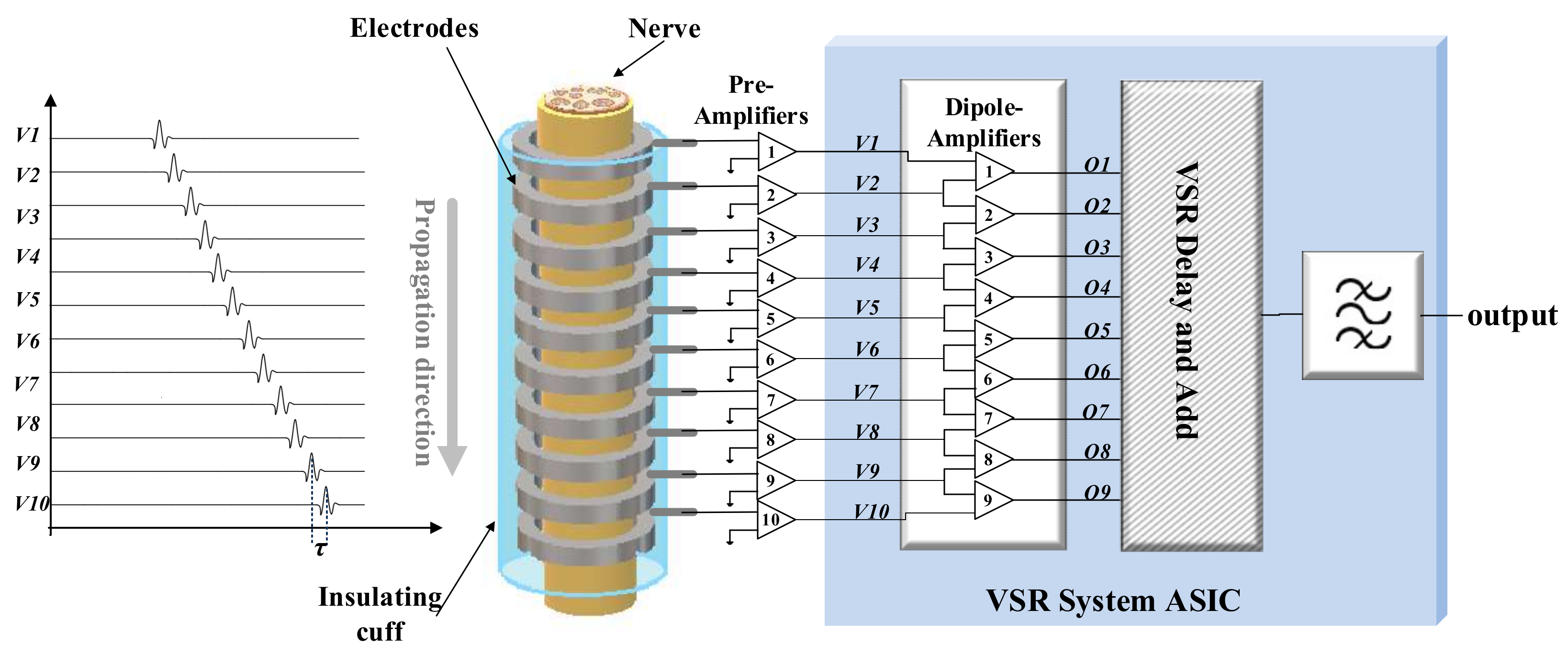
2.1. Basic Principles

The input to the MEC is a trans-membrane action potential function (TMAP), Vm(t), with the corresponding spectrum Vm(f). The resulting single-fibre action potential (SFAP) is a propagating wave with the time dependence of the underlying TMAP function, the relationship between the two being explained in [3]. We represent the TMAP function and its spectrum by the following Fourier transform pair [3]:
V m t = A t n e B t
V m ( f ) = n ! A ( B + j 2 π f ) n + 1
where A, B and n are constants and f is frequency (the symbology has been preserved from [3]). The output, Y(f, v), which is a function of both frequency and velocity, is obtained by treating the MEC as a linear time-invariant system with the transfer function H(f, v) [3].
Y f , v = G f , v H 0 f , v V m f
G(f, v) is the transfer function of the delay-and-add stage and H0(f, v) is the transfer function of a single dipole. At matched velocities (i.e., where the inserted system delay τ = d/v and v = v0), Y(f, v) approximates to
Y ( f , v 0 ) = 2 N R e R a sin π f d v 0 A ( B + j 2 π f ) 2
where Ra and Re are the intra- and extra-axonal resistances per unit length, respectively, and d is the electrode pitch. The output of the system, Y(f, v), is a function of two variables, and it was pointed out in [3] that if f is fixed by passing the output through a bandpass filter (so that f = f0), Y becomes a function of propagation velocity v only, enabling the velocity selectivity profile (see the tuning curves in [3]) to be calculated readily.
We define a velocity quality factor, Qv, by analogy with linear systems in the frequency domain where v0 is the matched (i.e., peak) velocity. Close to the matched velocities, the velocity selectivity is dominated by the function G(f, v) and the approximate formula for Qv is:
Q v N π d f 0 2.64 v 0
Figure 1 shows the front-end signal acquisition stages of a VSR system for recording signals from a 10-electrode cuff. The electrodes are shown grouped as N dipoles, although with extra circuitry a connection such as N − 1 tripoles is also possible. CVs in the approximate mammalian range of 20 ≤ v ≤ 100 m/s are considered. As already noted, the electrode array can be connected to the amplifiers using DC or AC coupling and, in addition, the coupling system may include bandpass filters to reduce the effects of ambient and RF interference (RFI) on the recorded signal.
The front-end system is followed by a delay-and-add stage that is the core of the system and has a transfer function, G(f, v), in (3). This is shown inside the grey box to the right of the figure and consists of N inserted delays (i.e., one per channel) and a summer. As reported elsewhere [3,4], this process cancels the naturally occurring delay experienced by an action potential (AP) as it propagates along the nerve (this delay depends on the inter-electrode spacing and, critically, the CV of the AP) by introducing programmable, artificial delays of opposite polarity. This cancellation is represented in (4). This method is closely related to the beam-forming methods used in certain types of synthetic aperture radar systems [4]. When the two sets of delays (i.e., natural and artificial) cancel, propagating APs add constructively and so the signal power at the output of the summer reaches a maximum. The conduction velocity (v) corresponding to this naturally occurring unit delay (τ) is called a ‘matched’ velocity and the two are related by the expression τ = d/v, where d is the inter-electrode spacing of the electrode array. If the unit delay generated by the system is Td in the arrangement shown in Figure 1, the actual delay inserted into each channel is (Ni)Td, where 0 ≤ i <N.
The delays inserted into each channel are therefore integer multiples of Td, and by sweeping Td, the complete velocity spectrum can be computed. The velocity spectrum obtained in this way is called the ‘intrinsic’ velocity spectrum (IVS) and is heavily dependent both on the characteristics of the delay-and-add system and on the form of the AP itself [13]. In Figure 1, a BPF is shown placed at the output of the summer, and the resulting modified spectrum (BPVS) has both enhanced velocity selectivity and relative independence from the characteristics of the AP [13,20].

2.2. System Architecture and Specification
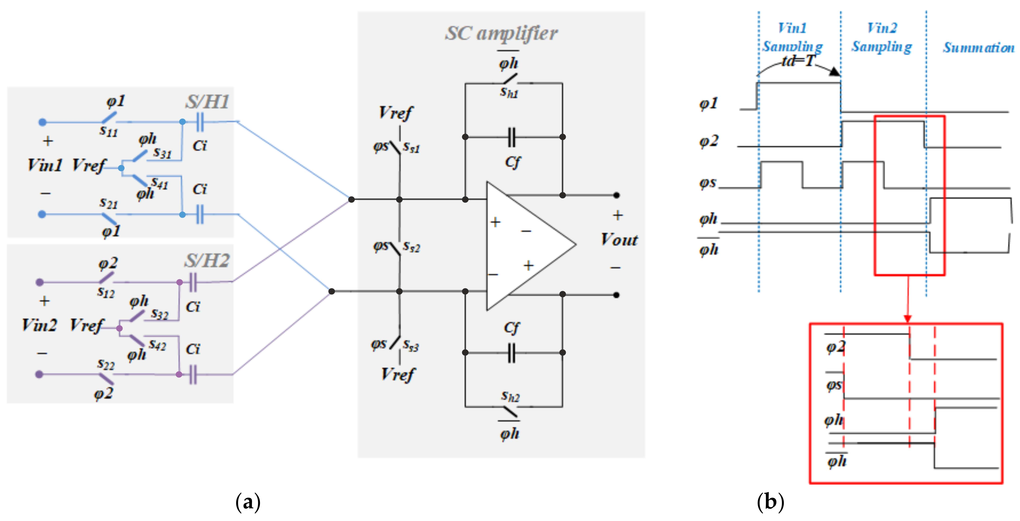
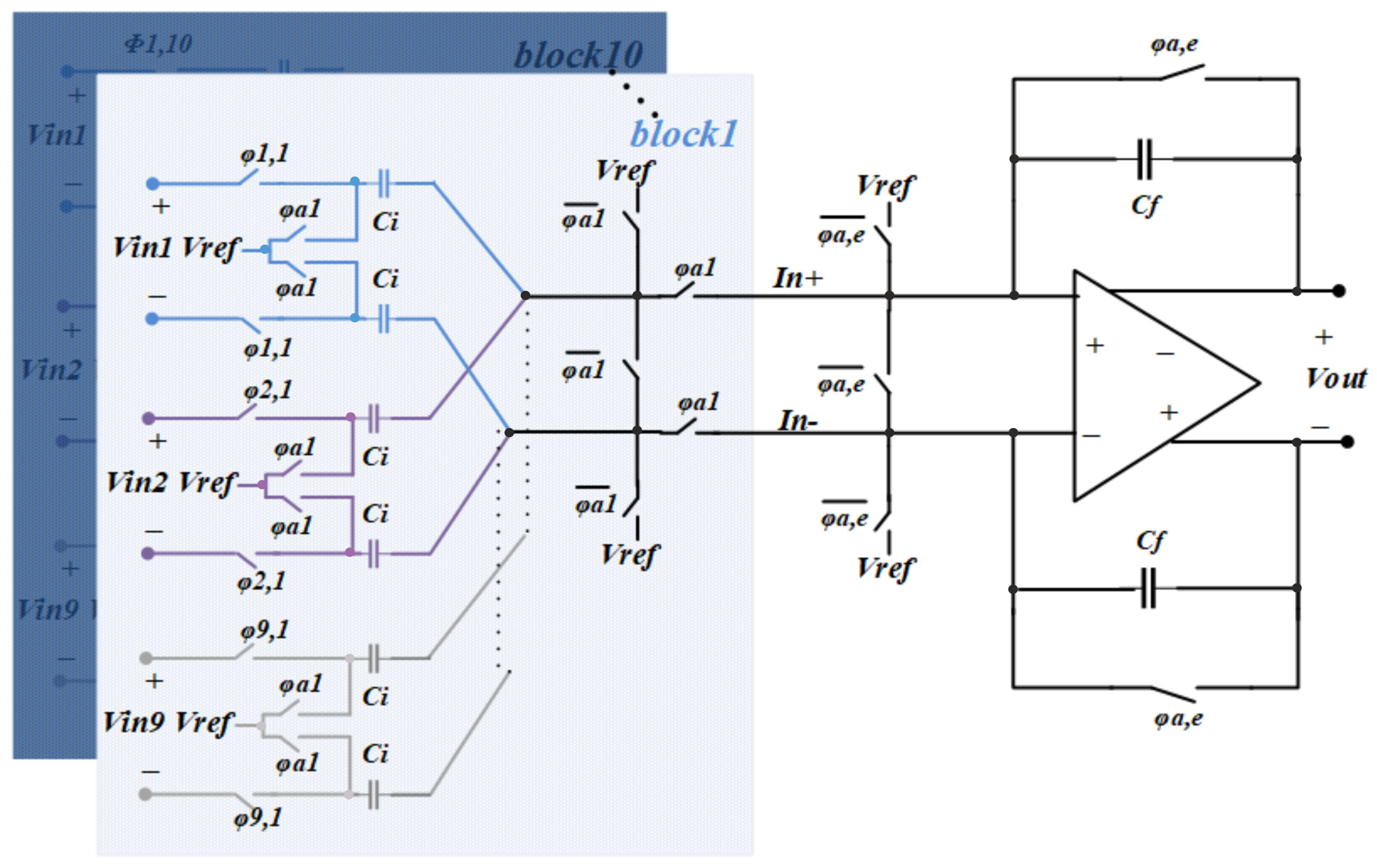
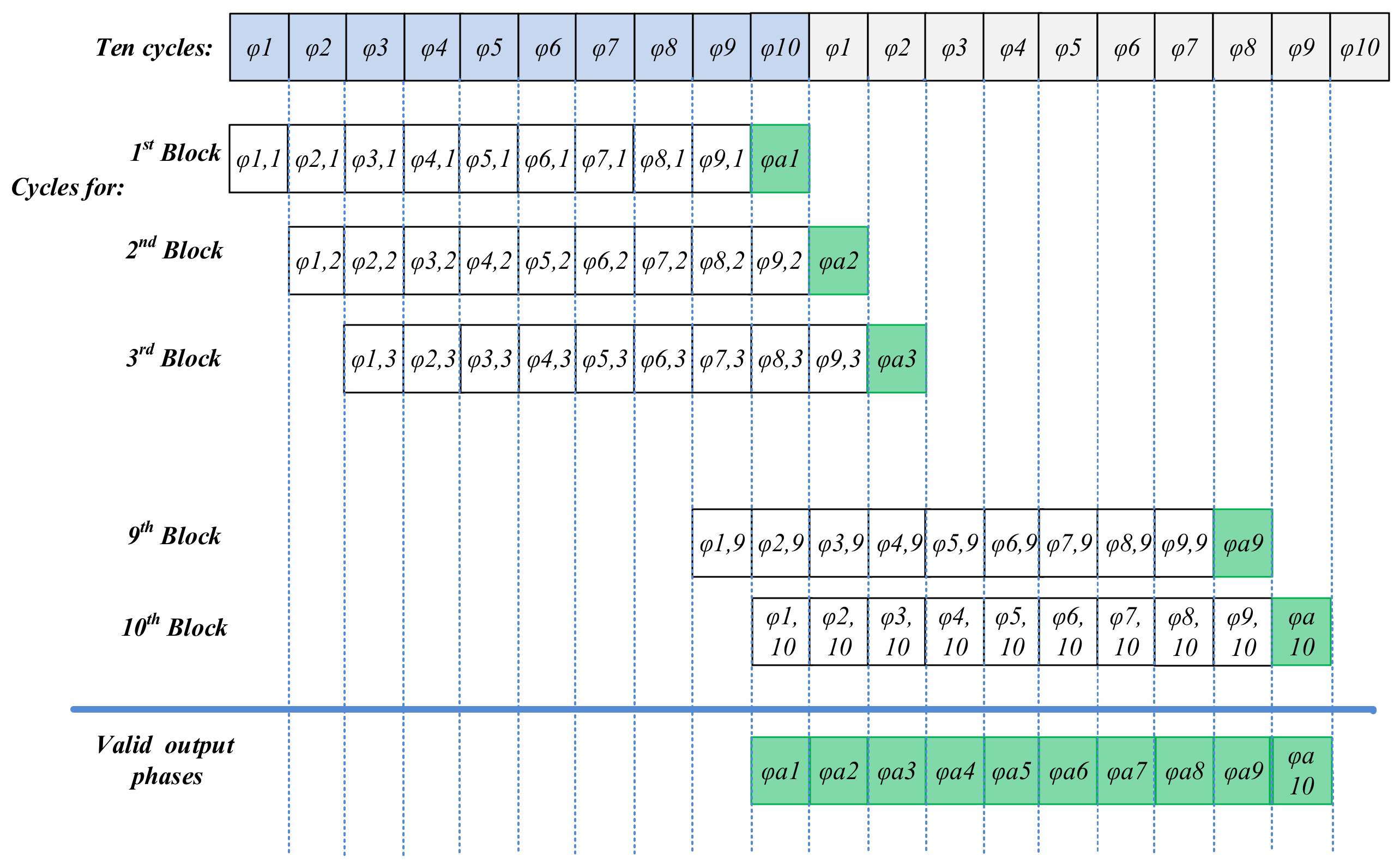
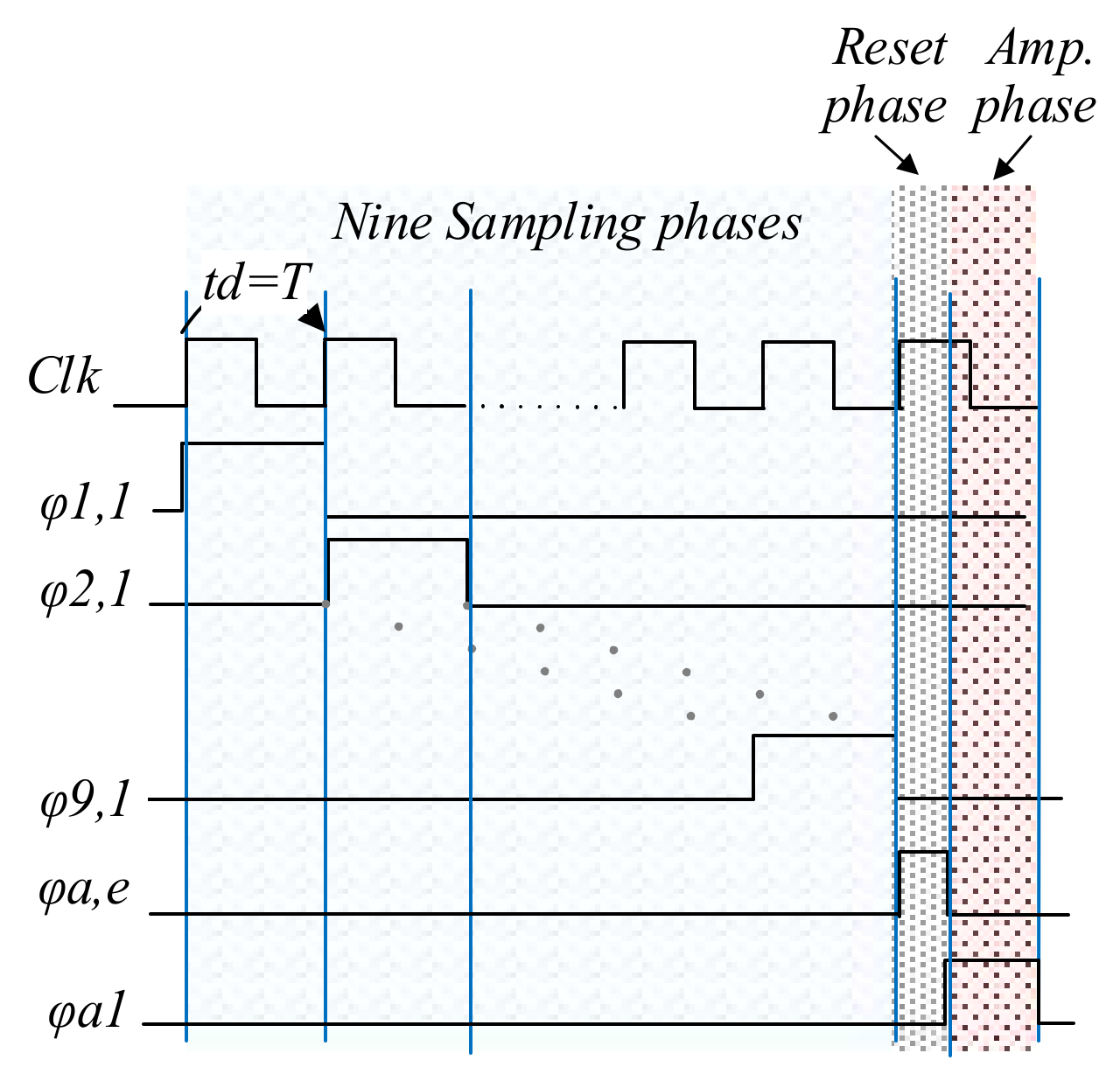
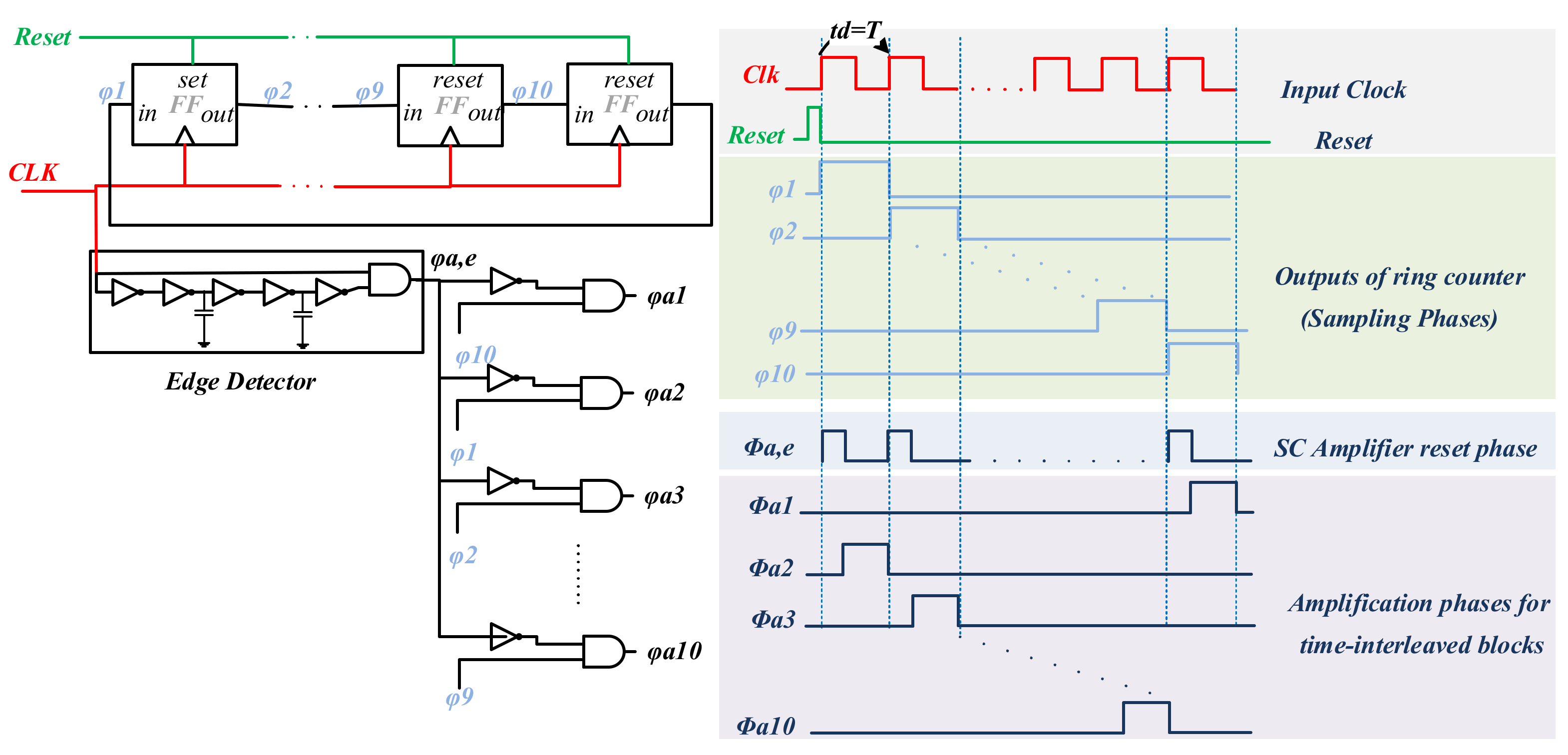
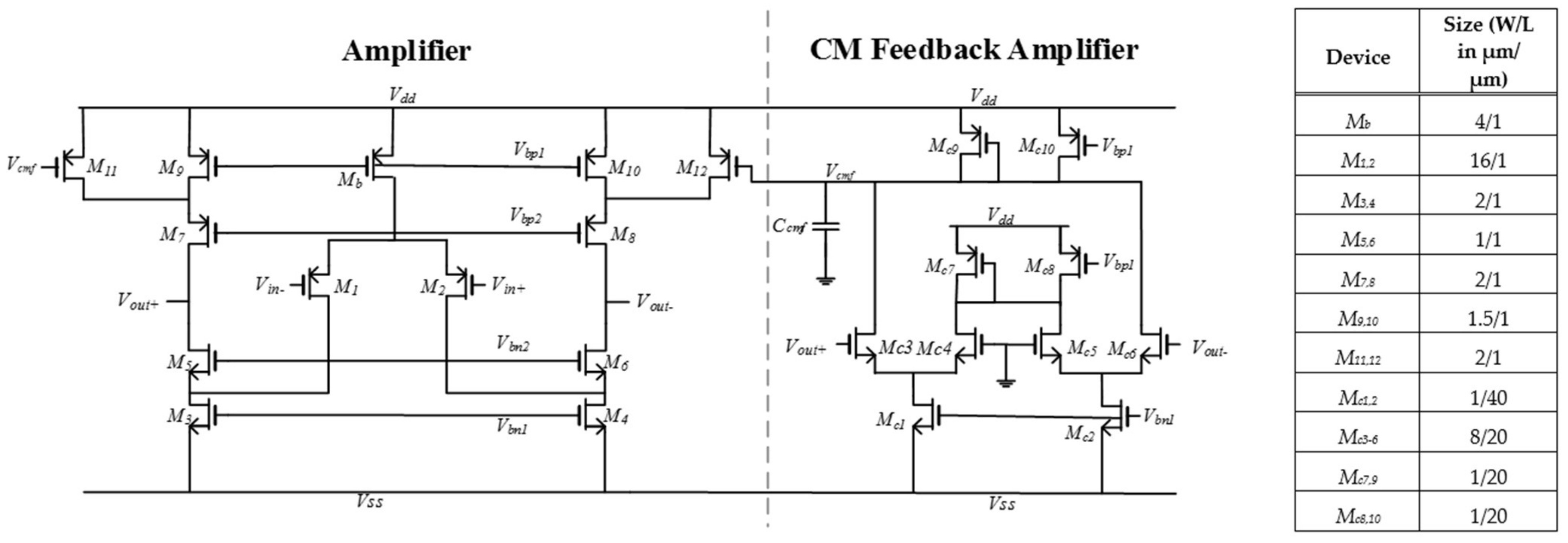
Although it is possible to realize a delay-and-add unit using digital technology, this is an expensive approach, which is significant, especially if an implanted system is required. Consider the case illustrated in Figure 1, where N + 1 = 10 analogue signals are obtained from the MEC and the inputs to the delay-and-add stage are the N = 9 dipolar outputs from the differential dipole amplifiers. As already noted, the delay appearing between these signals as they propagate along the MEC is given by the expression τ = d/v, and τ will be smallest for the highest CV being considered. For example, with d = 1 mm and v = 100 m/s, τ is required to be 10 µs, and so if an ADC is connected to each of these nine channels, as the interface to a digital delay-and-add system, each ADC will be required to complete its digitization within this period. This corresponds to a sampling rate of 100 k samples/s, a value that should be compared to what is required to digitize the analogue channel data directly. If the delay-and-add steps can be carried out in the analogue domain, digitizing only after addition and low-pass filtering using a single ADC, the advantages of the proposed method in terms of complexity and power consumption are very clear. For a typical analogue bandwidth of 10 kHz, a sampling rate of at least 20 k samples/s is required, which is clearly a significantly lower value compared to direct digitized data. The approach proposed in this paper uses switched-capacitor (SC) methods to sample the N + 1 pre-amplified analogue electrode signals and realize the delay-and-add function. Note that there is a one-to-one mapping between samples of the AP and points on the velocity spectrum. Therefore, in order to generate a spectrum with n points along the velocity axis, n cycles of delay-and-add are required.
Figure 2a is the schematic of a two channel (N = 1) sampling system realized using SC techniques that contains the important elements of a larger delay-and-add system. Note that the system can be extended for larger values of N by adding further differential SC sampling stages in parallel at the input to the differential summing amplifier. Figure 2b is the timing diagram. In comparison with our previous work [25], in which a delay-and-add system was presented for a two-channel recording system, the timing diagram for the switches has been modified to simplify the generation of control signals specially for the extended system with a higher number of channels presented here. Therefore, the control signal generation system has been implemented on chip using a ring counter and logic gates.
The circuit consists of a single differential SC amplifier whose inputs are provided by differential SC sample-and-hold (S/H) stages. Each S/H stage consists of a pair of capacitors (Ci) and two pairs of analogue sampling switches (sampling gates) with switching phases labelled φi (i = 1, 2 in this case). Since the sampling time of each S/H stage can be chosen independently, delays (Td) between the sampling points can be individually programmed. In addition to the input sampling switches (φi), another set of switches (φs) connect the inputs of the amplifier to the analogue ground potential (Vref), and, finally, a pair of switches whose phases are the complement of φh (i.e., φh) are connected across the integrating capacitors Cf. Note that a bottom plate sampling structure is used for the S/H circuits to improve linearity and accuracy by decreasing the nonlinear effects of charge redistribution by the sampling switches and the switch ON resistance [26]. The maximum ON resistance variation for the input-dependent switches S11S22 in Figure 2a is calculated to be 2.5%. Considering the time available for settling, the effect of the switches is negligible. For further clarification, the timing sequence between the control phases is shown in the zoomed view in Figure 2b. In the sampling phases, when the φi are ON and φs is also ON, the voltage on the input capacitors Ci tracks the input voltage. When φs turns OFF (φi and φh are still ON), the right-hand plates of the Ci are effectively floating (since the amplifier is connected as a differential buffer), and so the input voltage at the moment when φs turns OFF is stored on the Ci. This is the sampling point. Then, after a time interval, the φi switches turn OFF. At the sampling point, only the switches Ss1–3 turn OFF, and hence only the charge redistribution from the Ss1–3 switches affects the charge stored on the sampling capacitor. Since the voltages across these switches are constant, the charge added to the sampled value on Ci is constant for all input values. The sampling phase is followed, after an interval, by φh switching ON (and hence φh switching OFF so that the capacitors Cf are available to accumulate charge). At this point, the final phase of the cycle, the charge on all the Ci is accumulated on Cf and Vout is available. In our designed system, Cf and Ci have the same sizes. Therefore, each individual channel exhibits attenuation by a factor N, and summation of matched channels is possible using the full dynamic range.
The two-input system discussed previously [25] can readily be extended to higher orders by adding more S/H stages in parallel at the input to the differential summing SC amplifier. For example, Figure 3 shows the timing diagram for the structure extended to nine inputs. Note that, in this case, the output is valid only once in each ten cycles (φamp), i.e., after all samples have been taken and accumulated on Cf.
Assuming a consistent time interval (Td) across the array leads to a total time delay, (N − 1)Td. In order to meet the Nyquist criterion, the total time delay must satisfy (6):
( N 1 ) T d < 1 2 F m a x
where Fmax is the maximum frequency present in the input signal. Returning to the example quoted above, where N = 9, the minimum delay (i.e., τ = Td) required is 10 µs and the analogue bandwidth of the signal is 10 kHz, (N − 1)Td = 80 µs, whilst 1/(2Fmax) = 50 µs. Clearly, the Nyquist sampling requirement is not satisfied at any point in the required conduction velocity range (20 m/s–100 m/s). In order to satisfy the Nyquist sampling criterion at all points in the required velocity range, the delay-and-add system was modified to increase the sampling rate by time-interleaving ten S/H blocks connected in parallel [22]. In order to reduce power consumption, the summation is still carried out by one differential SC amplifier, which is shared between all ten blocks. The resulting nine-channel time-interleaved structure is shown in Figure 4. The interleaved S/H blocks are similar to the two-input system except for two extra series φa,x switches. These switches are added to disconnect the S/H stage from the amplifier in the sampling phase in order to allow the amplifier to be used by the other interleaved blocks. In addition, three further switches (φa,e) are added to the amplifier input to reset the amplifier at the beginning of each amplification phase.
The timing diagram for each block is shown in Figure 5. The sampling phases are illustrated in white, and the green intervals show amplification phases where the corresponding output is accumulated. The individual blocks operate with one cycle delay and add the inputs sequentially. The output is therefore valid in all cycles (φa1–10). As shown in Figure 5, all the sampling phases required for ten interleaved stages can be realized using ten clock phases (φ1–10).
Figure 6 shows the timing diagram of the control phases for the first time-interleaved block, shown in Figure 4 in order to discuss the timing for each block in detail. This circuit needs nine sampling phases for nine voltage inputs (φ1,1–9,1), a reset phase for the amplifier, in which the amplifier feedback capacitors are discharged (φa,e), and an amplification phase (φa1). In the two-input structure, the amplifier is reset in the sampling phase. This is not the case in the time-interleaved structure, since the amplifier is being used by one of the time-interleaved blocks in all the sampling phases, as illustrated in Figure 5. For example, if the amplifier is reset using φ9, it will no longer function as a switched-capacitor amplifier for block 10, since φ9,1 is the amplification phase for block 10. Therefore, a separate time interval (φa,e) is added at the beginning of each amplification phase to reset the amplifier.
As illustrated in Figure 5, all the sampling phases required for the time-interleaved structure are generated using ten clock phases (φ1–10). A detailed block diagram of the clock generation circuit is shown in Figure 7. The sampling phases are generated by a ring counter containing 10 delay elements (D-type flip-flops), all clocked by the signal Clk.

3. Circuit Design

The specifications of the low-noise pre-amplifiers [22] eventually preceding the VSR processing discussed here are not further described here. Two amplifier designs are employed in the proposed system following the front-end amplifiers: a folded-cascode SC amplifier and a separate unit used to define the common-mode level in the circuit. The SC amplifier and the common-mode feedback circuits are shown in Figure 8 with the device dimensions given in the table. With a power supply Vdd/Vss that is symmetrical around the ground reference (+/−1.5 V), the open-loop circuit yields a gain of 74 dB, a unity-gain bandwidth of 442 kHz with a phase margin of 65° and a CMRR of 50 dB. The input common-mode voltage range is −1.8 V (i.e., 300 mV below Vss) to 0.5 V. In order to design the amplifier in detail, the required transconductance and slew rate should first be determined. To operate the folded-cascode amplifier in an SC circuit, it is required that the amplifier output settles within the allocated phase period towards a specified error margin. The large-signal amplifier settling behaviour can be divided into two distinct phases, namely, a period during which the amplifier is slew-rate limited and a period during which it settles exponentially. A detailed analysis of this behaviour is presented in [27], giving an estimate for the duration (Tslew) of the slewing phase as
T s l e w V f s I b g m I b / C f C f V f s I b
where Ib is the maximum current that can be delivered to the output load, i.e., the tail current provided by transistor Mb in Figure 8, and Vfs is the maximum voltage input to the amplifier. The latter approximation holds for a Vfs larger than a few hundred millivolts, as is the case in this application. We have Ib as 5 µA, resulting in a gm of 50 µA/V. After the linear slewing period, the amplifier output settles exponentially with a time constant (τsettle) [28]:
τ s e t t l e 9 C i g m
To limit the settling error to less than 1% of the target value, a period of approximately 5τsettle is needed. Both slewing and exponential settling must be completed within the phase period Td/2. Using Cf = Ci = C and Vfs = 1 V, we hence have
5 τ s e t t l e + T s l e w < T d 2 45 C g m + C V f s I b < T d 2 C < T d 90 g m + 2 V f s I b
For our system, (9) commands a feedback capacitance less than 4.5 pF. This condition is well satisfied for the chosen Cf = Ci = 1 pF nominal capacitance, and it leaves room for accommodating parasitic effects and process variation. The system is followed by a buffer stage to drive measurement probes, which is not needed in a final system that interfaces directly to an analogue-to-digital converter or further processing stages on-chip. A differential NMOS pair with resistive load in an open-loop configuration is used as a buffer, in which the polysilicon resistor load is 6.1 kΩ and the transistors are biased so that the nominal voltage gain is approximately 7 v/v.

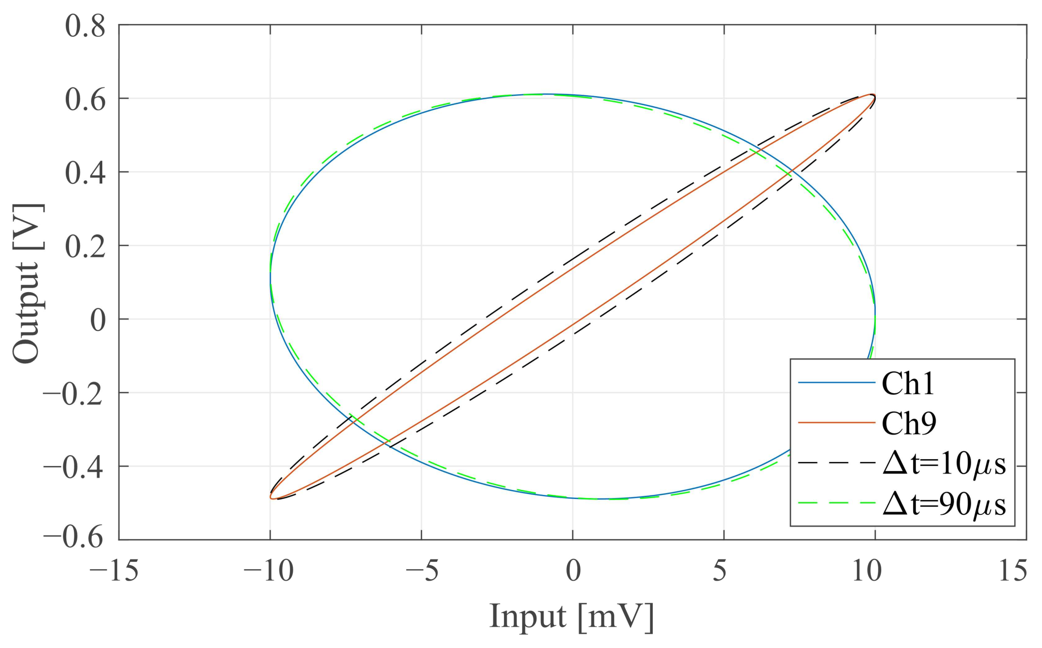
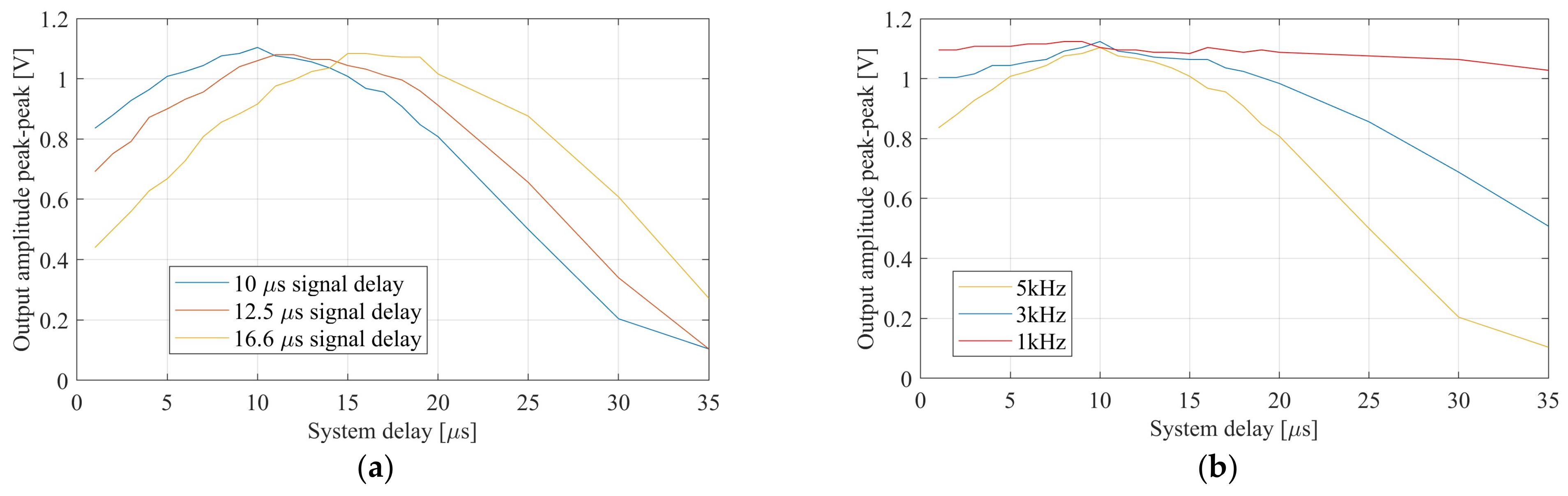
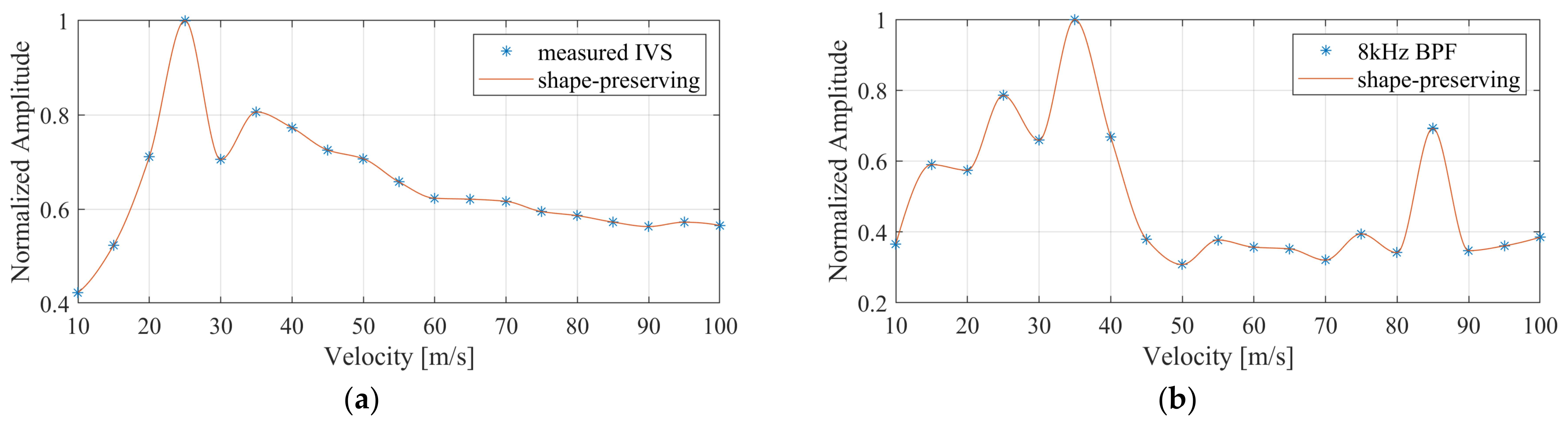
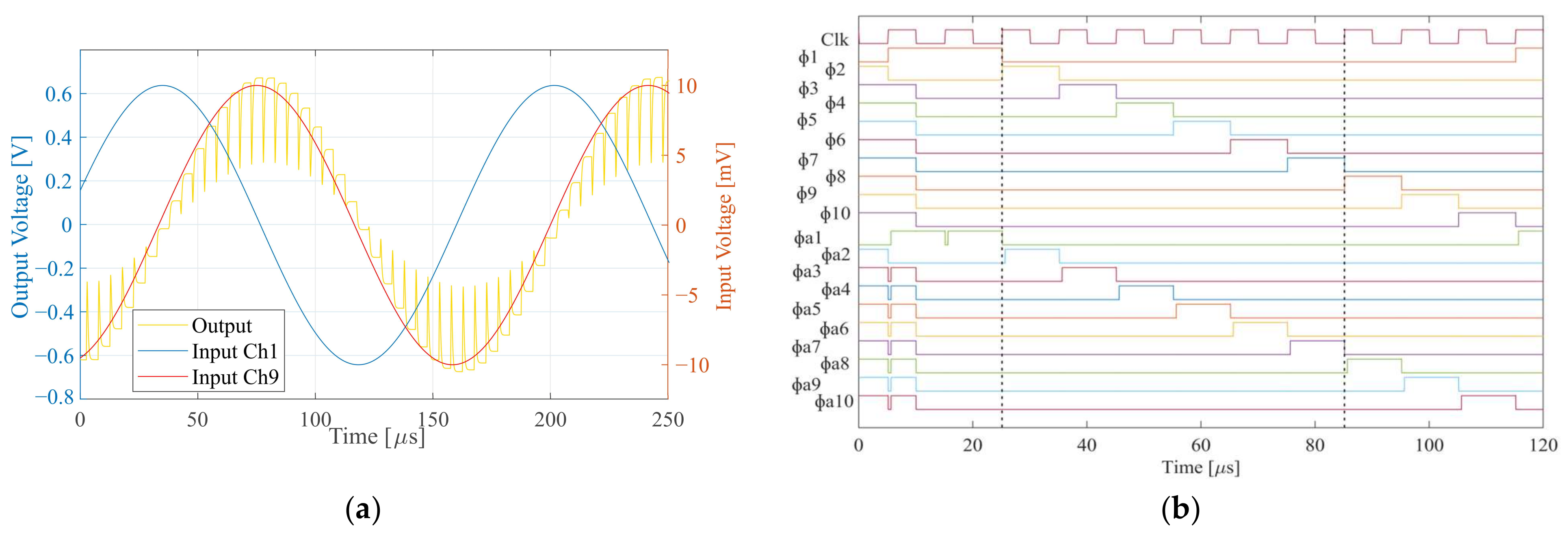
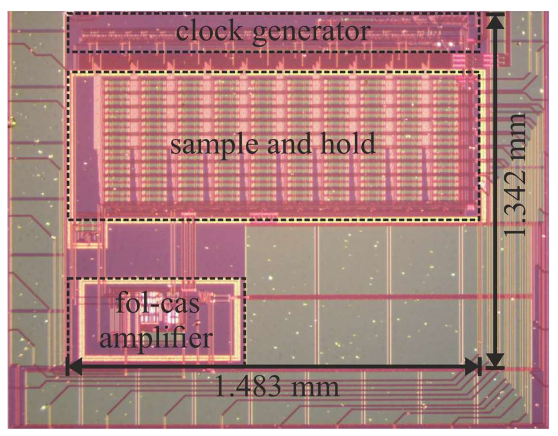
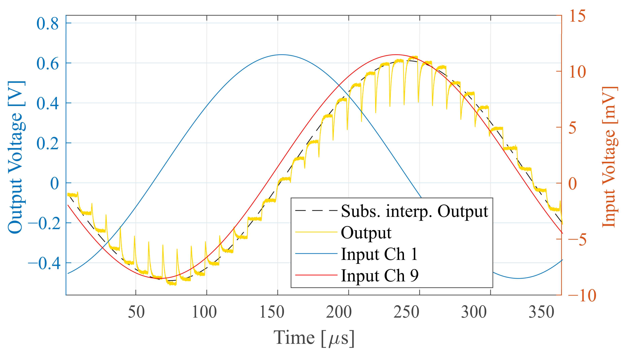
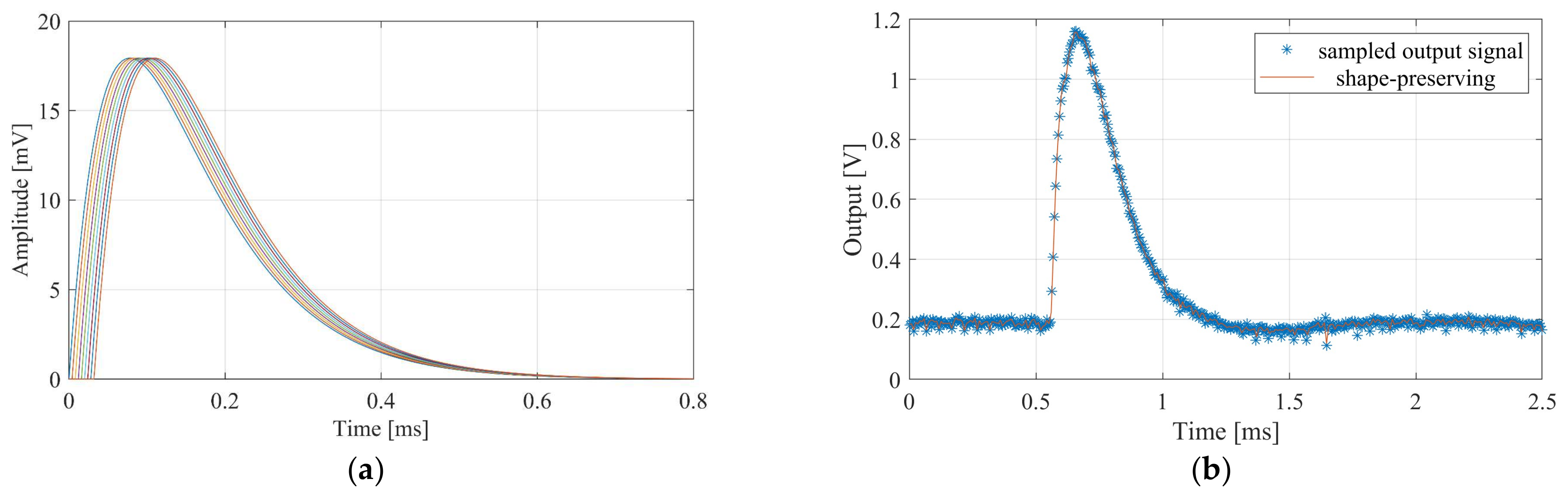
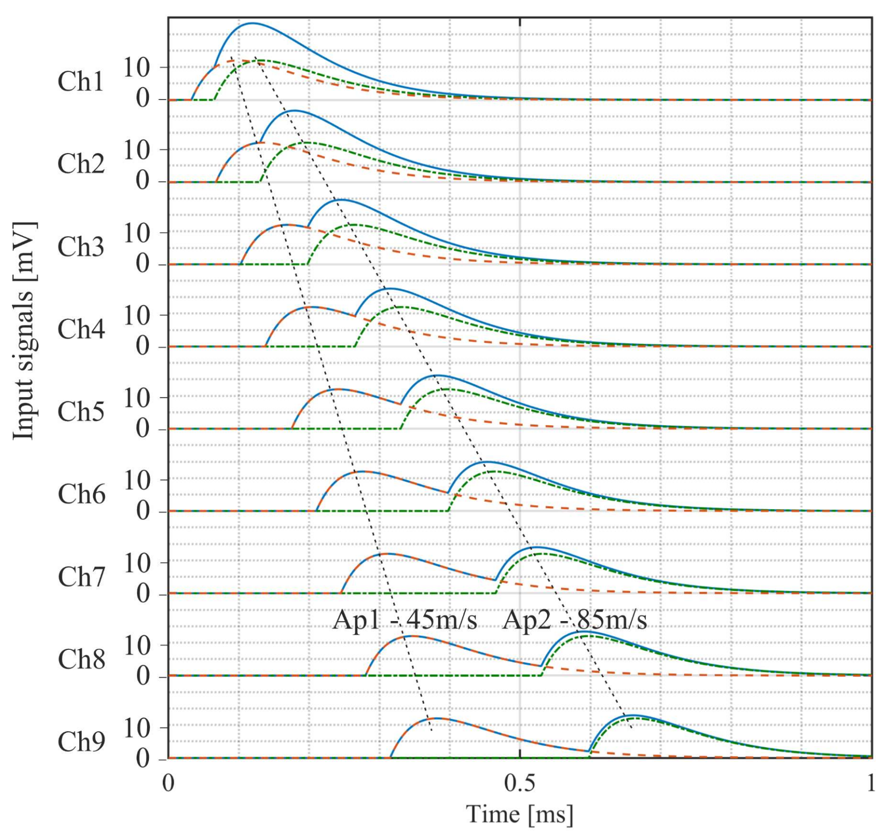
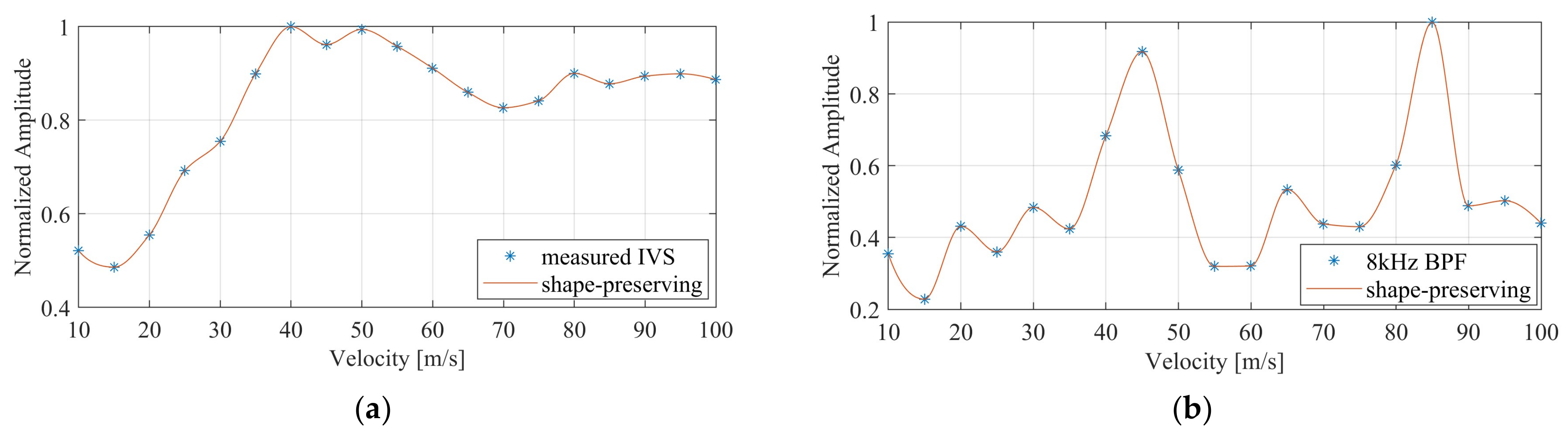
4. Simulated and Measured Results

The delay-and-add system of Figure 4 was implemented using a conventional single-well 0.35 µm CMOS technology. The supply voltage was 3 V (±1.5 V). The additional gain provided by the buffer stage defined by the on-chip resistor was expected to exhibit considerable inter-die variation. Simulations were carried out in the Cadence design environment using device models provided by the foundry. An exemplary system output response is presented in the transient simulation of Figure 9a, also showing the signal input for the outermost channels 1 and 9. All channels were driven by the same sinusoidal test signal with a frequency of 3 kHz and 20 mVpp amplitude, delayed by 10 µs between adjacent channels (i.e., the signal at channel 1 is delayed by 80 µs compared to channel 9). The timing diagram of the on-chip clock generator circuit for this setup is shown in Figure 9b. The circuit was controlled by the external clock signal (Clk) with a frequency of 100 kHz. As described before, the sample-and-hold phases of the input channels were derived from the positive edge of the signal Clk. In this simulation, since Td matched τ, addition of all channel amplitudes was expected. An amplitude increase by a factor of 63 (in the following, termed the signal gain of the system) compared to the single-channel input was observed in this simulation. This matched well with the expectation for the nine added channels and a buffer gain of 7 v/v. The overall average current consumption for the VSR circuit was 266 µA, resulting in a power consumption of 798 µW. An additional 1.65 mW was consumed by the output buffer used for testing.
Figure 10 shows a microphotograph of the fabricated ASIC active area. The locations of the folded-cascode amplifier, the sample-and-hold stage and the clock generator circuit are indicated. They occupy a silicon area of 1.164 mm2. For the following measurements, the ASIC was placed on a custom-made printed circuit board (PCB) and powered by a bench-top laboratory supply. External signals were generated with a PC-controlled data acquisition and generation (DAQ) card. A storage oscilloscope was used for probing the signals from which the graphs were generated using Matlab (R2018a, Mathworks, Natick, MA, USA) software.
First, the system was evaluated in the previously simulated configuration. The measured results corresponding to Figure 9a are shown in Figure 11. A superimposed dashed line shows the output signal interpolated from samples taken at a constant delay following the positive edge of signal Clk when the output has settled. It is representative of samples obtained from an ADC in a final mixed-signal system. The VSR system yields a gain of 55 v/v and consumes 2.53 mW of power, including the buffer. This is about 3% more than simulated, while the gain is 14% lower. Both deviations are within a range that can be attributed to a combination of process variation, mismatch and external bias source error.
Next, the delay between a 3 kHz sinusoidal test signal input as the reference and the system output was examined. Using the interpolated system output from Figure 11 and plotting it against the reference signal yielded Lissajous curves of the type shown in Figure 12. The figure exemplarily shows the extreme cases for channels 1 and 9. The longest delay is 90 µs on channel 1, and the shortest delay is 10 µs on channel 9. Up to a phase delay of 90°, the opening of the ellipse widens with increasing delay and it is tilted to the right. Above 90° (i.e., 83.3 µs for this test signal), the tilt moves toward the left and the opening begins to narrow. This behaviour was well observed in the measurements. Ideal shapes generated in Matlab are superimposed in Figure 12 and confirm the system performance. The slight deviation indicates that the measured delay was 2.5 µs longer than anticipated, indicating a sampling delay in the measurement equipment.
Also, the noise of the system was measured while it was operated with a 100 kHz clock and all channel inputs were grounded. The measured output noise was referred to the system input (IRN) by dividing through the gain of 55 v/v. The integrated IRN in the bandwidth from 10 Hz to 5 kHz was 7.0 µVrms. At 100 Hz, an IRN density of 200 nV/√Hz was observed, or about 67 nV/√Hz per channel. This was much lower than the output noise from the pre-amplifiers according to [22].
In a next step, the velocity selectivity of the system was tested by applying identical but artificially delayed sinusoidal test signals to the electrode inputs. Figure 13a shows plots of the measured peak-to-peak system output amplitude when a 5 kHz sine was used as the test input and the delay between electrodes was swept from 2 µs up to 35 µs, while the system delay was tuned to 10.0 µs, 12.5 µs and 16.6 µs by applying the appropriate clock frequency (Clk) (100 kHz, 80 kHz and 60 kHz), corresponding to 100 m/s, 80 m/s and 60 m/s for the assumed electrode pitch of 1 mm. The tuning curves thus obtained exhibit clear peaks where the artificial delay matches the system delay.
The tuning curve was expected to change for different test signal frequencies. The higher the frequency, the higher the quality factor according to (5), since no bandpass filter was applied here. In Figure 13b, three different input signal frequencies of 1 kHz, 3 kHz and 5 kHz were used and the corresponding tuning curves were plotted, confirming this principle relation.
Finally, the system was tested with artificially generated APs synthesized using the process established in [29]. The APs thus generated and played out using the DAQ card had a peak amplitude of 18 mV. Figure 14a shows the nine input signals and their inter-channel delay of 10 µs. For the matched clock frequency of 100 kHz, the sampled VSR system output is shown in Figure 14b. Also shown is the signal interpolated from the measured samples employing the shape-preserving spline function provided by Matlab. The measured output amplitude is 990 mV, which corresponds well to the initially measured gain of 55 v/v. Furthermore, the overall signal shape was well preserved after passing through the system. In a next step, the selectivity of the system with different AP velocities was examined. A superposition of two artificial APs with the same width and amplitude but different velocities (i.e., inter-channel delays) yielded the test signal shown in Figure 15. This was performed for a superposition of signals with a velocity of 45 m/s and 85 m/s and again for a superposition of 25 m/s and 35 m/s, assuming a cuff length of 30 mm and 10 electrodes. Each time, the test signal was applied repeatedly to the VSR system while the system delay was altered between measurements. The measured normalized intrinsic velocity spectra for the 45 m/s and 85 m/s APs are presented in Figure 16a. Although peaks at the expected velocities are visible, they are not very pronounced. Since it was established in [13] that the selectivity can be increased by applying bandpass filters at appropriate frequencies, a fourth-order bandpass with a fractional bandwidth of 20% and a centre frequency of 8 kHz was applied to yield the velocity spectrum in Figure 16b with more prominent peaks at the matched velocities of both APs. The corresponding spectra for the 25 m/s and 35 m/s APs are shown in Figure 17. Again, peaks are visible at the matched velocities. An additional, smaller peak is discernible in the filtered spectrum at 85 m/s. It is an artefact described in [13] caused by the bandpass filter.
To demonstrate the novelty and performance of the circuit presented here, Table 1 shows the progression of this VSR system compared to previous versions, both analogue and digital. The advantage of the analogue circuit over digital ones becomes markedly clear. The footprint of the system presented here is approximately 8% of the area required for the fully digital version presented in [23]. In [23,30], the clock signals were externally generated with a microcontroller (µC), whereas our system and the system presented in [25] use an on-chip integrated clock generator circuit. The detectable velocity bandwidth of the presented system is wider than that of all the other designs. While the VSR processing system presented here consumes more power and area per channel than the system in [25], this implementation allows for finer variation in system delay steps, resulting in a significant improvement in the relative velocity resolution. Since higher velocity resolution requires more storage cells (either holding capacitors in the analogue implementation or memory in the digital version), there is a consequential trade-off between circuit size and resolution. To quantify this, we define a figure of merit (FOM) as the product of the relative velocity resolution and the occupied area on a per channel basis. Table 1 shows that this work improves the FOM by a factor of 7.75 compared to the next best design [30] and uses less power per channel, even though the absolute power consumption is higher than that of the system presented in [23].
Overall, it can be shown that the system presented here excels in the following areas: detection velocity bandwidth, system delay bandwidth, system delay step size and relative velocity resolution.

5. Conclusions

This paper presents the first integrated analogue realization of the delay-and-add process for a nine-channel VSR system. By implementing the delay-and-add function in the analogue domain using switched-capacitor circuits, the proposed system overcomes the challenges associated with high-speed ADCs and the digital storage of multiple channels of delayed data. The sampled and low-pass-filtered data analogue approach enables the use of a single ADC for digitization, reducing complexity and power requirements. The results obtained from simulated and measured chips fabricated in 0.35 μm CMOS technology demonstrate the effectiveness of the proposed approach. The successful operation of the system was evaluated using simplified test vectors as well as synthetic nerve signals, demonstrating the extraction of velocity spectra. The VSR system described offers a practical and efficient solution for achieving velocity-selective nerve recordings with cuff electrodes.

Author Contributions

Conceptualization, R.R. and J.T.; methodology, S.S. (Shamin Sadrafshari), S.S. (Sebastian Simmich), R.R. and J.T.; validation, S.S. (Shamin Sadrafshari), S.S. (Sebastian Simmich), R.R. and J.T.; formal analysis, S.S. (Shamin Sadrafshari) and S.S. (Sebastian Simmich); investigation, S.S. (Shamin Sadrafshari) and S.S. (Sebastian Simmich); resources, R.R. and J.T.; data curation, S.S. (Shamin Sadrafshari), S.S. (Sebastian Simmich), R.R. and J.T.; writing—original draft preparation, S.S. (Shamin Sadrafshari), S.S. (Sebastian Simmich), R.R. and J.T.; writing—review and editing, S.S. (Shamin Sadrafshari), S.S. (Sebastian Simmich), B.M., J.P., N.G., N.D., R.R. and J.T.; visualization, S.S. (Shamin Sadrafshari), S.S. (Sebastian Simmich), R.R. and J.T.; supervision, R.R. and J.T.; project administration, R.R. and J.T.; funding acquisition, R.R. and J.T. All authors have read and agreed to the published version of the manuscript.

Funding

This work was funded by the Deutsche Forschungsgemeinschaft (DFG, German Research Foundation)—Project-ID 434434223—SFB 1461—and by the United Kingdom Engineering and Physical Sciences Research Council (EPSRC) under grant EP/P018947/1. We acknowledge financial support by Land Schleswig-Holstein within the funding programme Open Access Publikationsfonds.

Data Availability Statement

The original contributions presented in the study are included in the article, further inquiries can be directed to the corresponding author.

Conflicts of Interest

The authors declare no conflicts of interest.

References

  1. Brindley, G.; Rushton, D. Clinical Neurology: Neuroprostheses; Baillieres-Tindall: London, UK, 1995; Volume 14, Number 1. [Google Scholar]
  2. Chew, D.J.; Zhu, L.; Delivopoulos, E.; Minev, I.R.; Musick, K.M.; Mosse, C.A.; Craggs, M.; Donaldson, N.; Lacour, S.P.; McMahon, S.B. A microchannel neuroprosthesis for bladder control after spinal cord injury in rat. Sci. Transl. Med. 2013, 5, 210ra155. [Google Scholar] [CrossRef] [PubMed]
  3. Donaldson, N.; Rieger, R.; Schuettler, M.; Taylor, J. Noise and selectivity of velocity-selective multi-electrode nerve cuffs. Med. Biol. Eng. Comput. 2008, 46, 1005–1018. [Google Scholar] [CrossRef] [PubMed]
  4. Taylor, J.; Donaldson, N.; Winter, J. Multiple-electrode nerve cuffs for low-velocity and velocity-selective neural recording. Med. Biol. Eng. Comput. 2004, 42, 634–643. [Google Scholar] [CrossRef] [PubMed]
  5. Cho, Y.; Park, J.; Lee, C.; Lee, S. Recent progress on peripheral neural interface technology towards bioelectronic medicine. Bioelectron. Med. 2020, 6, 23. [Google Scholar] [CrossRef] [PubMed]
  6. Haugland, M.; Lickel, A.; Haase, J.; Sinkjær, T. Control of FES thumb force using slip information obtained from the cutaneous electroneurogram in quadriplegic man. IEEE Trans. Rehabil. Eng. 1999, 7, 215–227. [Google Scholar] [CrossRef]
  7. Haugland, M.K.; Hoffer, J.A. Artifact-free sensory nerve signals obtained from cuff electrodes during functional electrical stimulation of nearby muscles. IEEE Trans. Rehabil. Eng. 1994, 2, 37–40. [Google Scholar] [CrossRef]
  8. Haugland, M.; Lickel, A.; Riso, R.; Adamczyk, M.M.; Keith, M.; Jensen, I.L.; Haase, J.; Sinkjær, T. Restoration of lateral hand grasp using natural sensors. Artif. Organs 1997, 21, 250–253. [Google Scholar] [CrossRef]
  9. Haugland, M.; Hoffer, J. Slip information obtained from the cutaneous electroneurogram: Application in closed loop control of functional electrical stimulation. IEEE Trans. Rehab. Eng. 1994, 2, 29–36. [Google Scholar] [CrossRef]
  10. Haugland, M.K.; Hoffer, J.A.; Sinkjaer, T. Skin contact force information in sensory nerve signals recorded by implanted cuff electrodes. IEEE Trans. Rehabil. Eng. 1994, 2, 18–28. [Google Scholar] [CrossRef]
  11. Pflaum, C.; Riso, R.R.; Wiesspeiner, G. Performance of alternative amplifier configurations for tripolar nerve cuff recorded ENG. In Proceedings of the 18th Annual International Conference of the IEEE Engineering in Medicine and Biology Society, Amsterdam, The Netherlands, 31 October–3 November 1996; pp. 375–376. [Google Scholar]
  12. Koh, R.G.L.; Zariffa, J.; Jabban, L.; Yen, S.-C.; Donaldson, N.; Metcalfe, B.W. Tutorial: A guide to techniques for analysing recordings from the peripheral nervous system. J. Neural Eng. 2022, 19, 042001. [Google Scholar] [CrossRef]
  13. Taylor, J.; Schuettler, M.; Clarke, C.; Donaldson, N. A summary of the theory of velocity selective neural recording. In Proceedings of the Annual International Conference of the IEEE Engineering in Medicine and Biology Society, Boston, MA, USA, 30 August–3 September 2011; pp. 4649–4652. [Google Scholar]
  14. Metcalfe, B.W.; Hunter, A.J.; Graham-Harper-Cater, J.E.; Taylor, J.T. Array processing of neural signals recorded from the peripheral nervous system for the classification of action potentials. J. Neurosci. Methods 2021, 347, 108967. [Google Scholar] [CrossRef] [PubMed]
  15. Metcalfe, B.; Granger, N.; Prager, J.; Sadrafshari, S.; Grego, T.; Taylor, J.; Donaldson, N. Selective Recording of Urinary Bladder Fullness from the Extradural Sacral Roots. In Proceedings of the 2020 42nd Annual International Conference of the IEEE Engineering in Medicine & Biology Society (EMBC), Montreal, QC, Canada, 20–24 July 2020; pp. 3873–3876. [Google Scholar]
  16. Schuettler, M.; Donaldson, N.; Seetohul, V.; Taylor, J. Fibre-selective recording from the peripheral nerves of frogs using a multi-electrode cuff. J. Neural Eng. 2013, 10, 036016. [Google Scholar] [CrossRef] [PubMed]
  17. Yoshida, K.; Kurstjens, G.A.M.; Hennings, K. Experimental validation of the nerve conduction velocity selective recording technique using a multi-contact cuff electrode. Med. Eng. Phys. 2009, 31, 1261–1270. [Google Scholar] [CrossRef] [PubMed]
  18. Schuettler, M.; Seetohul, V.; Rijkhoff, N.J.; Moeller, F.V.; Donaldson, N.; Taylor, J. Fibre-selective recording from peripheral nerves using a multiple-contact cuff: Report on pilot pig experiments. In Proceedings of the 2011 Annual International Conference of the IEEE Engineering in Medicine and Biology Society, Boston, MA, USA, 30 August–3 September 2011; pp. 3103–3106. [Google Scholar]
  19. Jabban, L.; Ribeiro, M.; Andreis, F.R.; dos Santos Nielsen, T.G.N.; Metcalfe, B.W. Pig Ulnar Nerve Recording with Sinusoidal and Temporal Interference Stimulation. In Proceedings of the 2022 44th Annual International Conference of the IEEE Engineering in Medicine & Biology Society (EMBC), Glasgow, Scotland, 11–15 July 2022; pp. 5084–5088. [Google Scholar]
  20. Andreis, F.R.; Metcalfe, B.; Janjua, T.A.M.; Jensen, W.; Meijs, S.; Nielsen, T.G.N.d.S. The Use of the Velocity Selective Recording Technique to Reveal the Excitation Properties of the Ulnar Nerve in Pigs. Sensors 2021, 22, 58. [Google Scholar] [CrossRef] [PubMed]
  21. Karimi, F.; Seydnejad, S.R. Velocity Selective Neural Signal Recording Using a Space-Time Electrode Array. IEEE Trans. Neural Syst. Rehabil. Eng. 2015, 23, 837–848. [Google Scholar] [CrossRef] [PubMed]
  22. Rieger, R.; Schuettler, M.; Pal, D.; Clarke, C.; Langlois, P.; Taylor, J.; Donaldson, N. Very low-noise ENG amplifier system using CMOS technology. IEEE Trans. Neural Syst. Rehabil. Eng. 2006, 14, 427–437. [Google Scholar] [CrossRef]
  23. Clarke, C.T.; Xu, X.; Rieger, R.; Taylor, J.; Donaldson, N. An implanted system for multi-site nerve cuff-based ENG recording using velocity selectivity. Analog Integr. Circuits Signal Process. 2009, 58, 91–104. [Google Scholar] [CrossRef]
  24. Clarke, C.; Rieger, R.; Schuettler, M.; Donaldson, N.; Taylor, J. An implantable ENG detector with in-system velocity selective recording (vsr) capability. Med. Biol. Eng. Comput. 2017, 55, 885–895. [Google Scholar] [CrossRef]
  25. Rieger, R.; Taylor, J. Delay-line-based signal processing ASIC for velocity selective nerve recording. In Proceedings of the 2014 IEEE Asia Pacific Conference on Circuits and Systems (APCCAS), Ishigaki, Japan, 17–20 November 2014; pp. 205–208. [Google Scholar]
  26. Pelgrom, M.J.M. Analog-to-Digital Conversion; Springer: Berlin/Heidelberg, Germany, 2013. [Google Scholar]
  27. Chuang, C. Analysis of the settling behavior of an operational amplifier. IEEE J. Solid-State Circuits 1982, 17, 74–80. [Google Scholar] [CrossRef]
  28. Razavi, B. Design of Analog CMOS Integrated Circuits; Mc Graw Hill: New York, NY, USA, 2017. [Google Scholar]
  29. Rieger, R.; Schuettler, M.; Chuang, S.-C. A device for emulating cuff recordings of action potentials propagating along peripheral nerves. IEEE Trans. Neural Syst. Rehabil. Eng. 2014, 22, 937–945. [Google Scholar] [CrossRef]
  30. Rieger, R.; Taylor, J. A Switched-Capacitor Front-End for Velocity-Selective ENG Recording. IEEE Trans. Biomed. Circuits Syst. 2013, 7, 480–488. [Google Scholar] [CrossRef] [PubMed]
Figure 1. Schematic of a multi-channel VSR system for recording ENG signals from a 10-electrode cuff, configured as 9 dipole channels (i.e., N = 9). This paper focuses on the analogue VSR delay-and-add circuit (striped pattern) and does not consider either the pre-amplifiers or the dipole amplifiers since they have been previously reported elsewhere.
Electronics 13 00569 g001
Figure 2. (a) Schematic of an SC realization of a delay-and-add system with two differential inputs (N = 1). (b) Timing diagram for the system. The inputs are sampled onto the capacitors Ci for ultimate accumulation on the capacitors Cf.
Electronics 13 00569 g002
Figure 3. Timing diagram of the nine-channel delay-and-add circuit. One complete sampling cycle is shown. Note that the output is only available once in each ten cycles, when all the samples have been accumulated on Cf (indicated in green).
Electronics 13 00569 g003
Figure 4. Schematic of an SC realization of a delay-and-add system with nine inputs (N = 8), an extension of the circuit shown in Figure 2 (with N = 1). In order to increase the sampling rate and to meet the bandwidth requirements of the analogue input signals, 10 blocks of time-interleaved input sampling stages have been added in parallel.
Electronics 13 00569 g004
Figure 5. Timing diagram for a time-interleaved nine-channel VSR system. All the clock signals (φ1–10,x) are generated by ten non-overlapping pulses of width Td and period 10Td, delayed by Td from each other.
Electronics 13 00569 g005
Figure 6. Timing diagram of the control phases for the first time-interleaved input sampling stage block, shown in Figure 4.
Electronics 13 00569 g006
Figure 7. Control signal generator circuit. This consists of a synchronous ring counter using D-type flip-flops and some logic.
Electronics 13 00569 g007
Figure 8. Amplifier circuits and the corresponding component dimensions. The SC amplifier on the left is a folded-cascode design. The transconductance amplifier on the right is the CM stabilisation circuit.
Electronics 13 00569 g008
Figure 9. Nine-channel VSR system time domain simulation. (a) Time-delayed (10 µs) inputs of channels 1 and 9 and the corresponding sampled output. (b) Timing diagram of the on-chip clock generator circuit for an external clock signal of 100 kHz, representing 10 µs inter-channel delay.
Electronics 13 00569 g009
Figure 10. Microphotograph of the implemented nine-channel VSR system without the pre-amplifier stage.
Electronics 13 00569 g010
Figure 11. Measured signals for a sinusoidal input with a frequency of 3 kHz, the sampled output and a subsampled interpolated output signal.
Electronics 13 00569 g011
Figure 12. Measured Lissajous traces of channel 1 (90 µs delay) and channel 9 (10 µs delay) in comparison with the ideal delay (dashed ellipses).
Electronics 13 00569 g012
Figure 13. Measured output voltage peak to peak for a sinusoidal input signal. (a) Signal frequency of 5 kHz with different system delays. (b) Different input signal frequencies with the same inter-channel delay of 10 µs.
Electronics 13 00569 g013
Figure 14. (a) Artificially generated action potentials with an amplitude of 18 mV and a delay of 10 µs between adjacent channels as input to the nine-channel system. (b) Sampled and interpolated output of the system with a matched clock.
Electronics 13 00569 g014
Figure 15. Two synthetic action potentials with the same amplitude and different velocities—AP1 with 45 m/s (red dashed line) and AP2 with 85 m/s (green dotted–dashed line). Both action potentials were then superimposed to yield the test signals (blue line).
Electronics 13 00569 g015
Figure 16. Measured intrinsic velocity spectrum (a) and the 8 kHz fourth-order bandpass-filtered intrinsic velocity spectrum (b) for a combination of two artificially generated action potentials with velocities of 45 m/s and 85 m/s. The orange lines are shape-preserving fits through the measured data points.
Electronics 13 00569 g016
Figure 17. Measured intrinsic velocity spectrum (a) and the 8 kHz fourth-order bandpass-filtered intrinsic velocity spectrum (b) for a combination of two artificially generated action potentials with velocities of 25 m/s and 35 m/s. The orange lines are shape-preserving fits through the measured data points.
Electronics 13 00569 g017
Table 1. Measured digital and analogue delay-and-add performance comparison without a pre-amplifier stage.
This Work[25][30][23]
Channel98210
Technology (µm)0.350.350.80.8
Gain (dB)36-36.5-
IRN/ch (nV/√Hz)67-14 *-
Sample and HoldAnalogueAnalogueAnalogueDigital
Detection Velocity (m/s)10–30016–12039–3001–30
Clock GeneratorIntegratedIntegratedµCµC
System Delay Td (µs)10–30010–1005–80100–3000
Δ Td (µs)1–300105–80100
Rel. Velocity
Resolution
0.003–0.090.09–0.50.06–0.20.03–0.5
Power/ch (µW)9122.51400>13,000
Area/ch (mm2)0.1290.09750.051.6
FOM (µm2)3878775300048,000
* Measured with a pre-amplifier.
Disclaimer/Publisher’s Note: The statements, opinions and data contained in all publications are solely those of the individual author(s) and contributor(s) and not of MDPI and/or the editor(s). MDPI and/or the editor(s) disclaim responsibility for any injury to people or property resulting from any ideas, methods, instructions or products referred to in the content.

