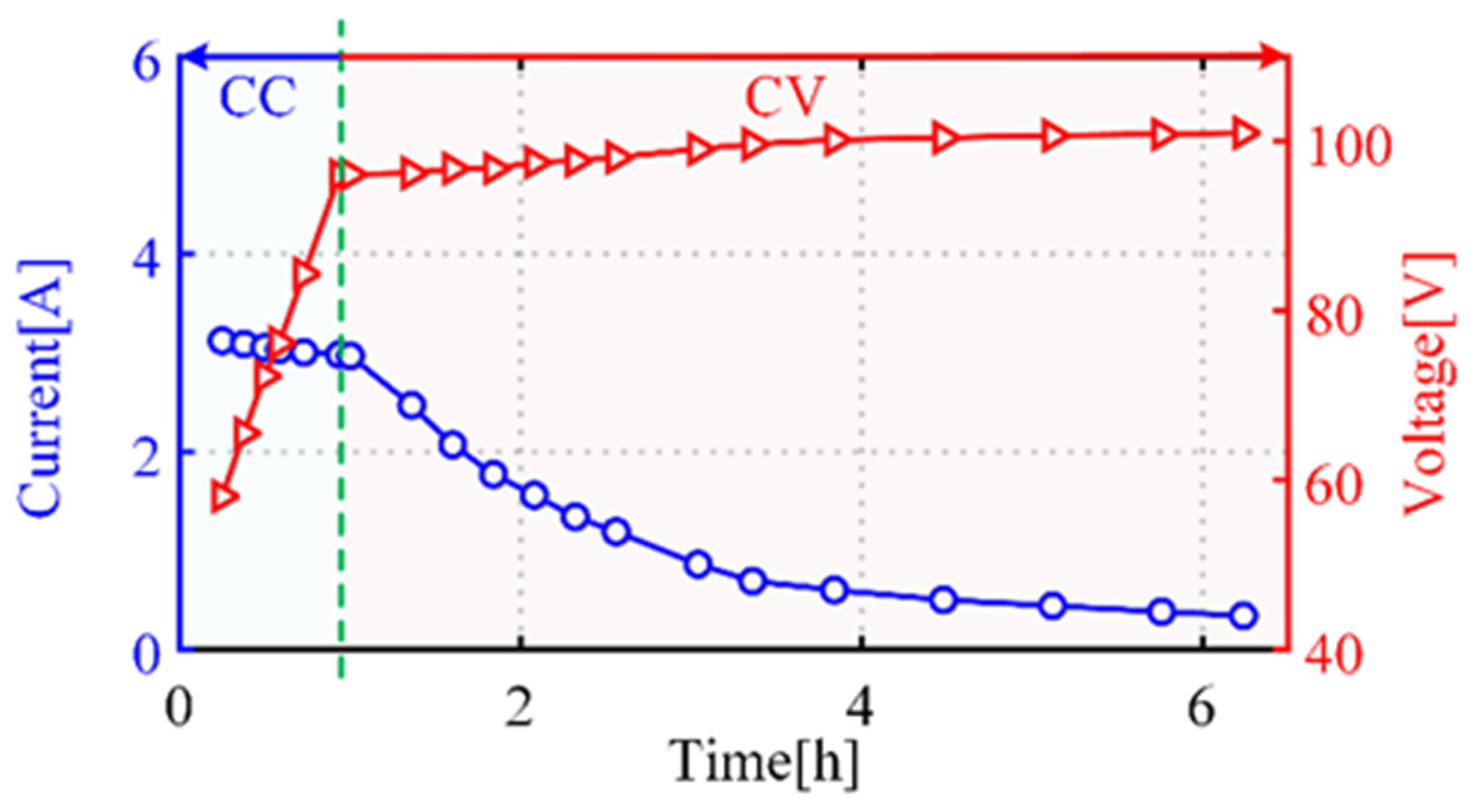
Article

Wide-Load-Range Double-T Resonant Converter for CC/CV Battery Charging

1
School of Electrical and Information Engineering, Tianjin University, Tianjin 300072, China
2
Beijing Aerospace Automatic Control Institute, Beijing 100854, China
*
Author to whom correspondence should be addressed.
Electronics 2024, 13(3), 533; https://doi.org/10.3390/electronics13030533
Submission received: 19 December 2023 / Revised: 19 January 2024 / Accepted: 23 January 2024 / Published: 29 January 2024

Abstract

:
This article proposes a load-independent constant current (CC) or constant voltage (CV) output Double-T circuit (DT) for electrical vehicles (EVs) or electrical bikes (EBs) charging systems to improve the conversion efficiency over a wide-load range during battery charging processes. Among available studies, the LLC converter is a widely adopted resonant topology for EV or EB charging. However, in CC-CV charging, the wide output voltage caused by the wide-load range requires a wide switching frequency range to achieve, which decreases the efficiency in the wide-load range. To address such issues, in this article, two T-circuits are cascaded to form an output load-independent DT with fixed duty cycle and frequency, which can implement CC-CV modes and zero phase angle at the resonant frequency simultaneously, which not only significantly reduces reactive power in energy storage elements but also eliminates the adverse effect of efficiency reduction owing to switching frequency variation. Finally, based on experimental results, the variation of current in CC mode is within 4.18%, and that of voltage is within 4.44% in CV mode, which demonstrates the inherent load-independent capability of the DT converter. During the battery pack charging experiment, the peak dc-dc conversion efficiency reached 96.70% and the average conversion efficiency was higher than 94.01%.

1. Introduction

In recent decades, the number of vehicles with internal combustion engines (ICE) on the road around the world has seen explosive growth [1,2,3]. However, the extensive use of fossil fuels and the emission of pollutant gas deteriorates numerous damages to the environment and human society. In this background, the application of electrical vehicles (EVs) and electrical bikes (EBs) has been particularly supported by many policymakers and governments for their environmental friendliness [4,5]. It is predicted that there will be 500 million passenger EVs and many more EBs worldwide by 2040 [6]. As EVs and EBs rely on electric energy stored in batteries, battery chargers have become a focus of many institutions. A high-performance rechargeable lithium-ion battery is currently identified as a suitable and competitive candidate for EVs and EBs nowadays and its typical charging profile is depicted in Figure 1. Typically, the charging process can be divided into two charging stages [7]: first, the constant current (CC) charging stage; second, the constant voltage (CV) charging stage, meanwhile, the battery equivalent resistance is also variable during the charging process. Nevertheless, the common battery chargers can mostly charge the battery with the constant output current or voltage, which will not only shorten the battery life and compromise cycle life but also affect the safety and performance of batteries [8,9]. To address these issues, it is essential to design a battery charger that can respond to the battery’s characteristics by altering the CC or CV output mode and maintaining high conversion efficiency across a wide range of load resistances.
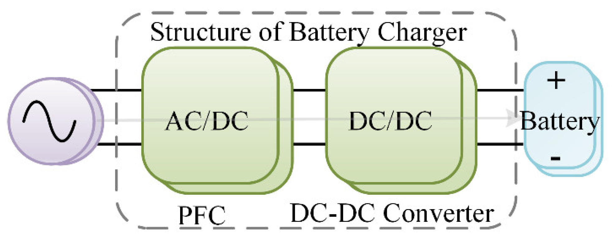
As shown in Figure 2, the common rechargeable battery chargers are composed of two basic parts [10]: an ac-dc converter with power factor correction (PFC) function part and a dc-dc resonant converter part widely used to modulate the output of the battery chargers. Thus, the dc-dc converter is the key to the battery chargers. Among the many topologies of the dc-dc converters, the LLC topology is a popular candidate for dc-dc converter by means of the inherent advantages, such as zero-voltage-switching (ZVS) for MOSFETs of the inverter, zero-current-switching (ZCS) for diodes of the rectifier and simple structure [11,12,13]. However, for common LLC converters which usually adopt pulse frequency modulation (PFM) control, wide load variation in battery charging can result in a wide output voltage range, which requires a corresponding wide variation range of switching frequency accordingly [14]. Nevertheless, if the switching frequency deviates from the resonant frequency, the converter will lose its zero-phase angle (ZPA) conditions and the soft switching features, resulting in increased reactive power loss and switching loss, which in turn leads to a rapid decrease in conversion efficiency. Additionally, the wide switching frequency range expands the demands on the design of transformers and gate drivers, as well as other power equipment [15]. Designing the dc-dc converters for wide load range applications, particularly those that can implement CC-CV modes and achieve high conversion efficiency for battery charging applications, can be challenging. Various technologies have been proposed to address these difficulties, which can be divided into two categories.
The first category can be concluded as the design of modulation strategies. These strategies present various modulation control strategies that are commonly used in LLC converters to narrow the switching frequency range. In [16], a hybrid modulation control method combined with PFM and phase shift (PS) is proposed, which can enhance the efficiency and output controllability of the LLC converters. However, hybrid modulation is not suitable for a wide output range, hybrid converters frequently rely on PFM during heavy loads, resulting in variable switching frequencies that may induce power loss and resonance deviation-related magnetizing component problems. To achieve a higher voltage gain over the same frequency range, in [17,18], symmetric pulse width modulation (SPWM) is adopted in the MOSFETs on the primary side, which permits the system to broaden or narrow the extra voltage range by controlling the duty cycle. However, the high demand for gate drivers and inverters significantly limits its development. Meanwhile, the extra output range is constrained by the duty cycle and the ZVS conditions.
In the second category, the methods are not limited to the optimization for modulation algorithm but focus on the design and optimization for the new topology and realization of wide load operation of dc-dc converters and CC-CV output modes. In [19] a new topology based on LLC is proposed to obtain higher voltage gain in a narrower frequency. Although it shrinks the frequency range, the issues associated with PFM remain and the light load power is low. In [20], a PEV charger is implemented with a wide output voltage range by means of changing the dc-link voltage through the first PFC stage, which can extremely narrow the range of frequency. However, traditional boost topology cannot meet the design requirements, and the sophisticated measurements and control strategy also limit the application. To further address the above issues and implement the CC-CV output mode, some articles are devoted to the topology transform, which transforms the structures of the dc-dc resonant converter to modulate the output mode of them. In [21,22], a dc-dc resonant converter with switchable full-bridge and half-bridge parts by controlling the state of AC switches is proposed. Building on this work, Refs. [23,24], respectively, proposed variable capacitors and variable inductors control strategies to further optimize the system and implement the switching of CC-CV modes charging process. Although both of these methods allow for a narrow frequency range, even a fixed frequency, the complexity of control and measurement significantly limits their application. Additionally, the non-resonant state of the control process reduces conversion efficiency.
In summary, although the aforementioned methods can broaden the output range and can implement CC-CV output modes with narrow or fixed frequency. However, since their resonant topologies are all based on LLC, which leads to inherent issues, such as low conversion efficiency in a wide-load range and complexity in algorithm or measurement components still exist. To address these issues, this article proposes a dc-dc converter with a DT as the resonant circuit. Furthermore, a summary of the main contributions of this article is as follows:
(1)
The paper describes the theoretical derivation of the T-circuit, which demonstrates that the load-independent frequency can be the same as the resonant frequency through the proposed parametric configuration. This means that the T-circuit can theoretically achieve CC and CV output near the resonant frequency. By deploying AC switches and variable capacitors, the proposed DT converter can operate and switch between CC and CV modes at the resonant frequency.
(2)
Owing to the inherent load-independent characteristics of DT, the inverter on the primary side can operate at a fixed frequency with a constant duty cycle without any additional real-time control scheme and complexity measurement devices.
(3)
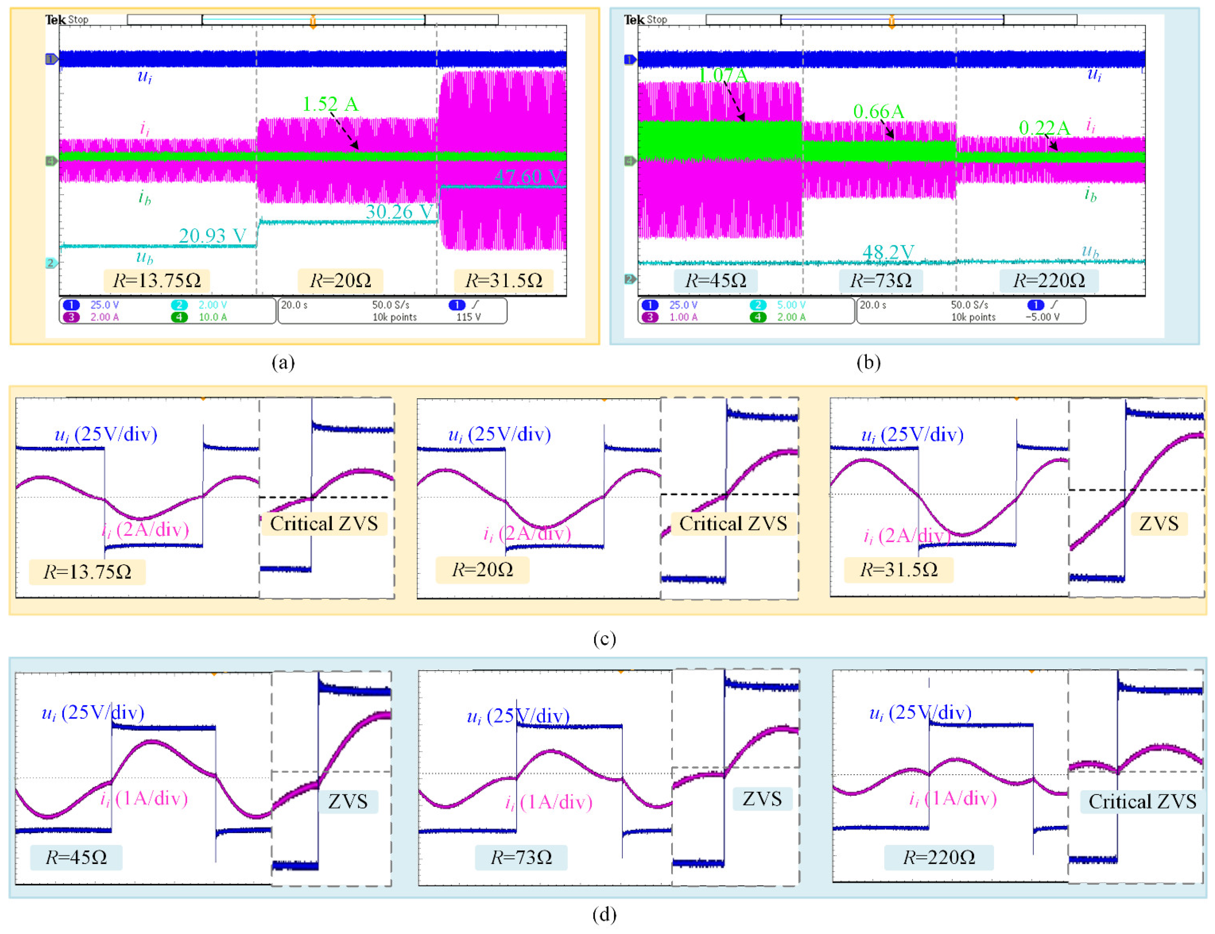
Based on experimental results, firstly, critical ZVS can be achieved in both CC and CV modes by carefully designing the DT resonant converter, which can significantly reduce switching losses. Secondly, the DT converter operates at the fixed resonant frequency regardless of CC and CV mode, which not only eliminates the issues caused by PFM but also reduces the circulating energy losses. The above two factors guarantee the high conversion efficiency of the system under various load conditions.

2. DT Characteristics Analysis

In this section, the basic characteristics of the DT are derived and demonstrated. In addition, the parametric configuration design methods for CC/CV and ZPA are discussed and it is demonstrated that with this proposed configuration scheme the DT can achieve CC/CV at a fixed resonant frequency under the input ZPA condition.
The schematic of the dc-dc converter with a DT as the resonant circuit is depicted in Figure 3. Obviously, several LC filters, such as L11 and C11, are adopted in the DT to replace the commonly used several capacitors. By replacement of the capacitors with LC filters, the total harmonic distortion (THD) will decrease. Meanwhile, the low THD also improves the accuracy of fundamental harmonic analysis (FHA), especially in CC mode [24]. In addition, the replacement is not necessary, and this paper chooses to replace LC filters for the generality of the parametric analysis. It should be noted that the above functions can be achieved in the actual design process as long as the following impedance conditions are met.

2.1. Basic Characteristics of DT Topology

Since several capacitors and inductors are adopted in the DT, for the sake of simplification, in this article, a parameter design method is proposed and used to represent the value of the components by using the relationship between the parallel inductor L13 or L23 and the series capacitors or inductors. β and γ, respectively, represent the impedance ratio of inductance, capacitance, and parallel inductance. The basic characteristics of the DT using this method can be defined as follows:
β 11 = L 11 L 13 , β 12 = L 12 L 13 β 21 = L 21 L 23 , β 22 = L 22 L 23 γ 11 = 1 ω 2 C 11 L 13 , γ 12 = 1 ω 2 C 12 L 13 γ 21 = 1 ω 2 C 21 L 23 , γ 22 = 1 ω 2 C 22 L 23 Z 11 = j ( ω L 11 1 ω C 11 ) = j ( β 11 γ 11 ) ω L 13 Z 12 = j ( ω L 12 1 ω C 12 ) = j ( β 12 γ 12 ) ω L 13 Z 13 = j ω L 13 Z 21 = j ( ω L 21 1 ω C 21 ) = j ( β 21 γ 21 ) ω L 23 Z 22 = j ( ω L 22 1 ω C 22 ) = j ( β 22 γ 22 ) ω L 23 Z 23 = j ω L 23
where the first number represents the parameter belonging to which T-circuit and the second number represents the position in that T-circuit. And Z is the impedance of each part accordingly.

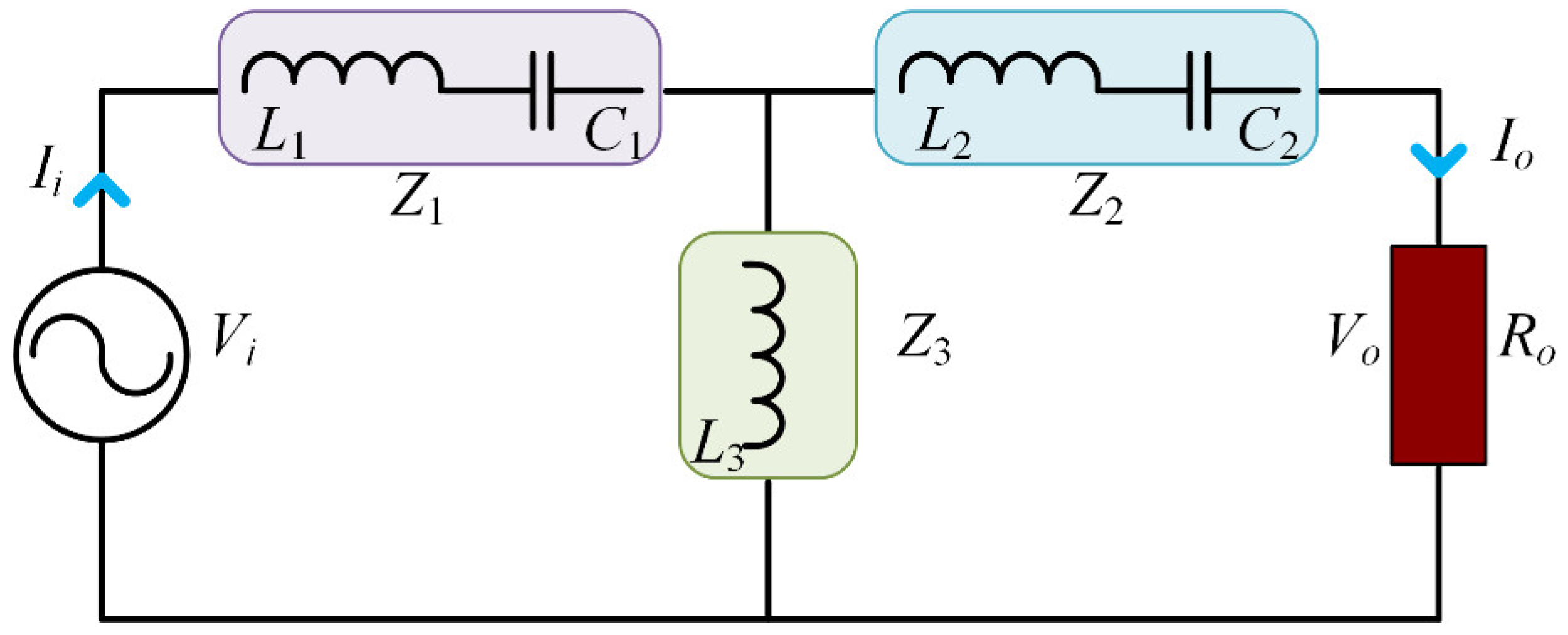
2.2. Output Characteristic Analysis of T-Circuit Topology

It is obvious that the DT is cascaded by two T-circuits. Therefore, systematically analyzing the output characteristic of the T-circuit is vitally important and necessary to figure out that of the DT. The equivalent circuit of the T-circuit using FHA is depicted in Figure 4. Vi is the fundamental voltage component of the square wave generated by the full-bridge inverter. Ii is the input current of the T-circuit. Vo and Io are the output current and voltage of the T-circuit. Ro is the load resistance of the T-circuit.
The noted reciprocity of the T-circuit means that a T-circuit can be designed as a voltage source or a current source by changing the parameters of the circuit. Accordingly, the voltage and current characteristics of the T-circuit are derived in the following part. To simplify the theoretical analysis process, the following part adopts the method proposed in (1), but only one T-circuit is analyzed, so the subscript has also only one number label. For example, Z 1 = j ω L 1 1 / ω C 1 = j β 1 γ 1 ω L 3 .
According to Kirchhoff’s voltage law (KVL), describing T-circuit as following equations:
V i ˙ 0 = Z 1 + Z 3 Z 3 Z 3 R o + Z 2 + Z 3 I ˙ i I ˙ o
Further, the output voltage and current can be deduced as equations of the input voltage and current:
V ˙ o = V ˙ i R 0 Z 3 R o ( Z 1 + Z 3 ) + Z 1 Z 3 + Z 1 Z 2 + Z 2 Z 3 ,
I ˙ o = V ˙ i Z 3 R o ( Z 1 + Z 3 ) + Z 1 Z 3 + Z 1 Z 2 + Z 2 Z 3 ,
V ˙ o = I ˙ i R 0 Z 3 R o + Z 2 + Z 3 , I ˙ o = I ˙ i Z 3 R o + Z 2 + Z 3 .
The input current also can be deduced as:
I ˙ i = V ˙ i ( R o + Z 2 + Z 3 ) R o ( Z 1 + Z 3 ) + Z 1 Z 3 + Z 1 Z 2 + Z 2 Z 3 .
Consequently, the input impedance of the T-circuit can be derived as:
Z i n = R o ( Z 1 + Z 3 ) + Z 1 Z 3 + Z 1 Z 2 + Z 2 Z 3 ( R o + Z 2 + Z 3 ) .
Then, the voltage gain of T-circuit GVV and the current gain of T-circuit GII can be expressed by
G V V = V ˙ o V ˙ i = R o Z 3 R o ( Z 1 + Z 3 ) + Z 1 Z 3 + Z 1 Z 2 + Z 2 Z 3 ,
G I I = I ˙ o I ˙ i = Z 3 R o + Z 2 + Z 3 .
Likewise, the transfer impedance of T-circuit GIV and transfer admittance GVI of the T-circuit can be described by
G I V = V ˙ o I ˙ i = R 0 Z 3 R o + Z 2 + Z 3 ,
G V I = I ˙ o V ˙ i = Z 3 R o ( Z 1 + Z 3 ) + Z 1 Z 3 + Z 1 Z 2 + Z 2 Z 3 .
where the first letter represents the input side, and the second letter represents the output side. For example, the current gain of T-circuit GII is the magnitude of the ratio of output current Io and input current Ii.

2.2.1. Constant Output Current Mode Analysis

This subsection introduces the condition of the T-circuit for achieving the CC output mode, namely, configuration Z1, Z2, or Z3 to make the output current of the T-circuit independent of the load. According to GVI and GIV, the CC output mode can be derived as:
Z 1 = Z 3 .
The parameters are expressed as:
γ 1 β 1 = 1 .
Then, substituting (8) into GVI, the new transfer admittance can be calculated as:
G V I Z 1 = Z 3 = I ˙ o V ˙ i = 1 Z 3 .
As for the current driven T-circuit, according to GII, it is clear that the Ro located in the denominator of GII has no coefficient, thus, the T-circuit cannot achieve the CC output mode under this condition.
In conclusion, a T-circuit driven by a voltage source can achieve the CC mode when γ 2 β 2 = 1 . Meanwhile, according to (5), the ZPA condition of the T-circuit can be calculated as:
Z 1 = Z 2 = Z 3 .
Therefore, a T-circuit can implement the CC output mode in case of input ZPA conditions, when the parameters are configurated as:
γ 1 β 1 = γ 2 β 2 = 1 .

2.2.2. Constant Output Voltage Mode Analysis

This subsection discusses the condition of the T-circuit for realizing the CV output mode.
From GVV, when driven by a voltage source, the T-circuit can achieve the CV output mode by satisfying the following equation:
Z 1 = Z 2 Z 3 Z 2 + Z 3 ,
Three available parameter configuration options can be solved:
Z 1 = Z 2 Z 3 Z 2 + Z 3 ,
Z 2 = Z 1 Z 3 Z 1 + Z 3 ,
Z 3 = Z 1 Z 2 Z 1 + Z 2 .
However, ZPA cannot be achieved under either of the above three conditions according to (11). Similarly, after solving GIV, the CV output mode can be achieved by
Z 2 = Z 3 .
The parameters are expressed as:
γ 2 β 2 = 1 .
Further, the new transfer impedance can be defined as:
G I V Z 2 = Z 3 = V ˙ o I ˙ i = Z 3 .
As a result, a T-circuit driven by a current source can achieve the CV output model and maintain input ZPA under γ 1 β 1 = γ 2 β 2 = 1 , but a T-circuit driven by a voltage source cannot. However, normal systems are driven by a voltage source, meanwhile, a lot of control schemes are proposed to commonly control the input voltage, which constrains the practical and applicable abilities of a T-circuit driven by a current source to achieve the CV output mode. Fortunately, according to GVI and GIV by cascading two T-circuits, a new voltage gain GVIIV can be defined as:
G V I I V = G V I G I V = Z 13 Z i n ( Z 11 + Z 13 ) + Z 11 Z 13 + Z 11 Z 12 + Z 12 Z 13 R o Z 23 R o + Z 22 + Z 23
where Z13 is Z3 of the first T-circuit, Z23 is Z3 of the second T-circuit. Then substituting the load-independent conditions (15) of the two T-circuits, the voltage gain of DT GVIIV can be calculated as:
G V I I V Z 12 = Z 13 , Z 22 = Z 23 = G V I G I V = Z 23 Z 13 .
Meanwhile, the parameters can be designed as:
γ 12 β 12 = γ 22 β 22 = 1 .
In summary, two T-circuits driven by a voltage source can achieve CV output mode and ZPA simultaneously, when the parameters are set to
γ 11 β 11 = γ 12 β 12 = 1 ,
γ 21 β 21 = γ 22 β 22 = 1 .
By comparing the conditions of realizing CC mode and ZPA conditions (12), it can be found that under the above conditions (21), either of the two cascaded T-circuits can also achieve CC mode and ZPA conditions.

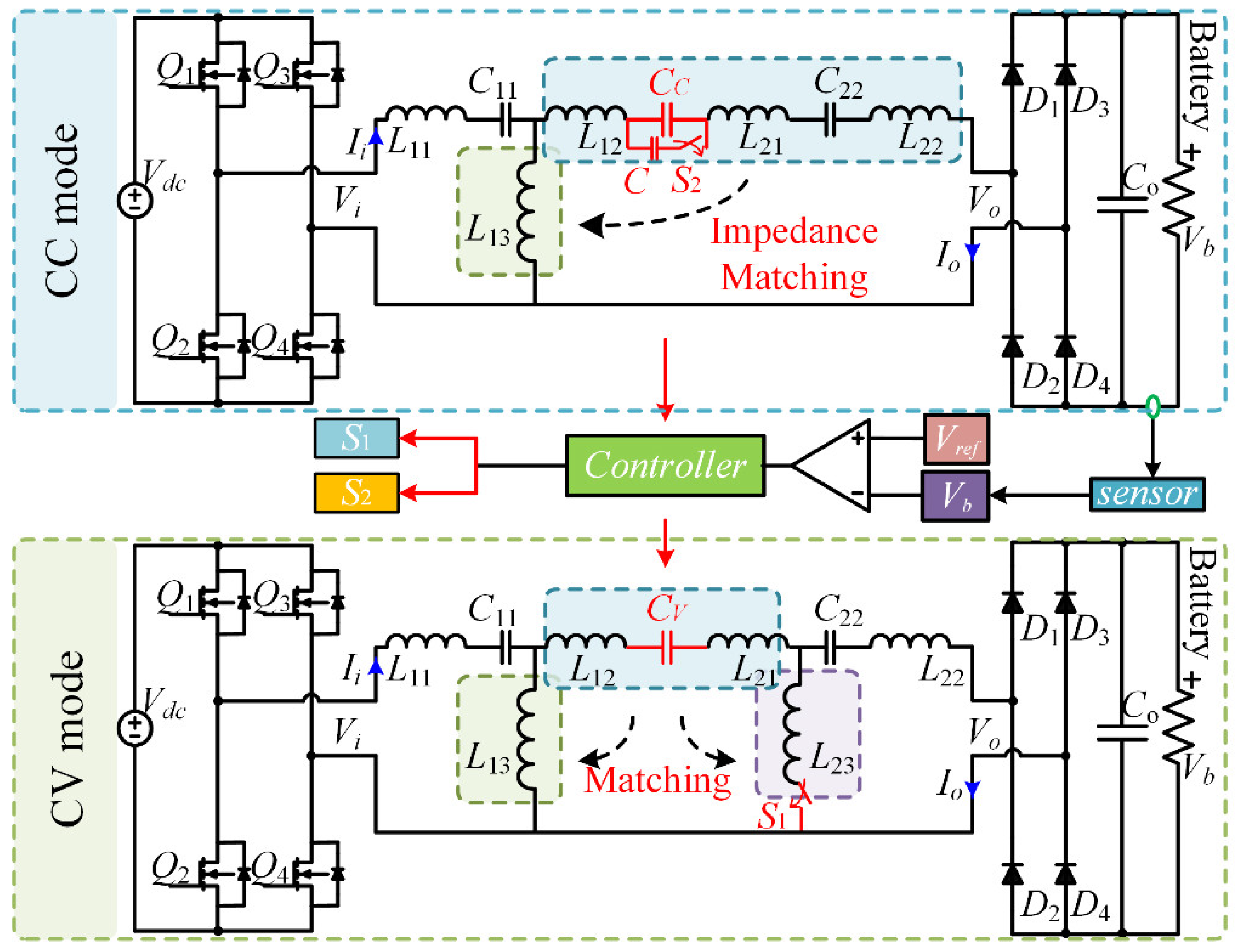
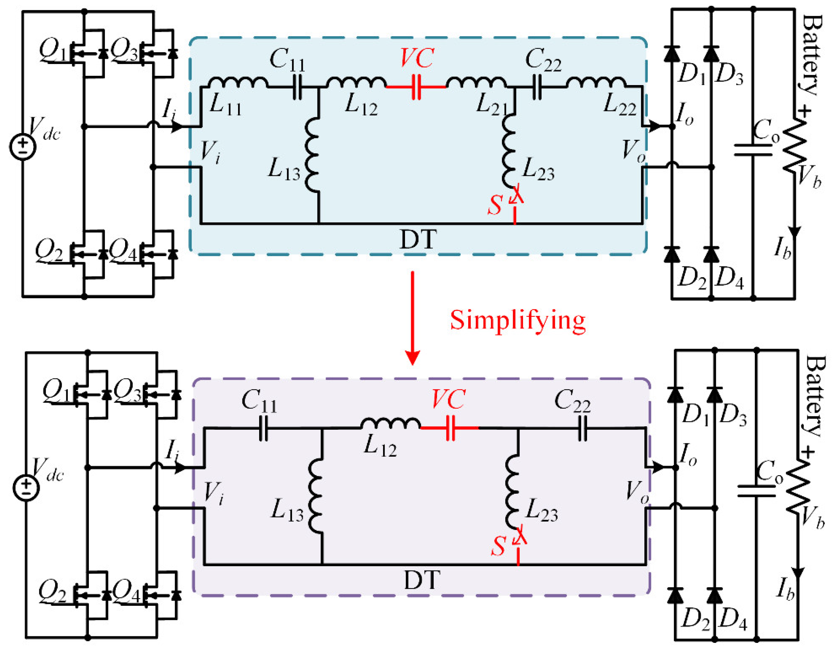
3. Implementation of DT with CC and CV Output Modes

This section demonstrates the topology-switching strategy of the DT and the parameter design method. Based on the results of the above analysis in Section 2, through designing the parameters β and γ, the T-circuit can achieve CC and CV modes under ZPA conditions at the resonant frequency. However, a single T-circuit cannot switch from CC/CV mode without changing the driver source, which is impossible for normal charging systems. To address the CC/CV switching issue, a DT with ACs and a variable capacitor (VC) is designed. The ACs consist of two MOSFETs connected in anti-series and the variable capacitor is comprised of a capacitor in parallel with a switching capacitor, which is a MOSFET S2 connected with a capacitor in series. As shown in Figure 5, the proposed DT can implement the CC/CV mode switching by controlling the on/off of the ACs S and the capacitance of the variable capacitor VC.

3.1. Switching Strategy of the dc-dc Converter

According to Figure 5, when the DT operates in CC output mode, it is necessary to disconnect the parallel inductor L23 of the second T-circuit from the DT. Thus, during the CC output mode, the ACs S1 will be controlled under off conditions. Simultaneously, upon disconnecting the L23 from the DT, the inductor L21, L22, and capacitor C22 in series in the second T-circuit will be connected to the output branch of the first T-circuit. Meanwhile, the capacitance of variable capacitor C will also be increased it capacitance value by turning on the S2 to maintain the impedance of the output branch matching the parallel branch, which determines the achievement of the ZPA and CC output mode. While operating under the CV output mode in Figure 5, the ACs S1 should be turned on to connect inductor L23. At this moment, the DT is cascaded with two T-circuits. The variable capacitor should, respectively, decrease the capacitance by turning off the S2 to match the impedance of the two parallel branches of the DT to keep the ZPA and CV output conditions.
Refer to Figure 5 for the switching strategy diagram. When the battery voltage increases to its maximum voltage in CC mode with the increase in the battery resistance, the amplifier will send a signal to the controller. The controller will execute corresponding operations on the ACs S1 and change the capacitance of variable capacitor VC by S2 to switch DT from CC to CV output mode. Figure 6 also displays the operating modes of the variable capacitor and S2.

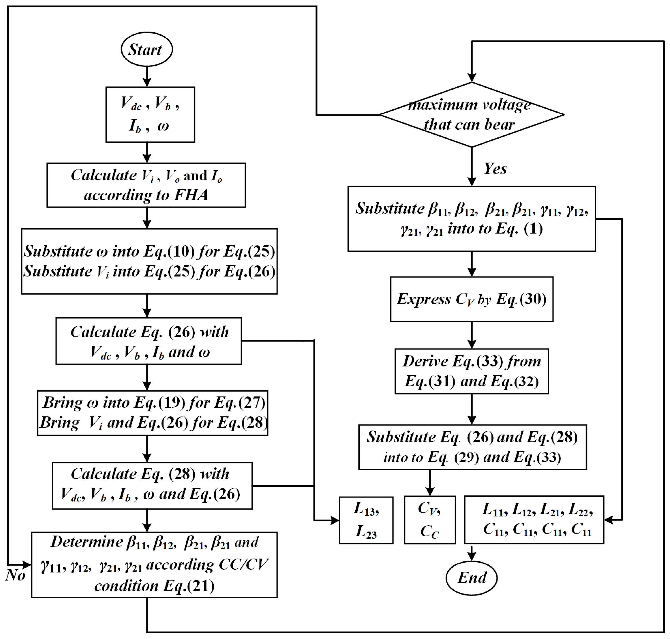
3.2. Parameters Design for DT Charger

The parameters of DT can be derived by the following design method. Typically, as for a battery charger, the dc link voltage Vdc, battery current (current of CC mode) Ib, battery voltage (voltage of CV mode) Vb, switching angle frequency ω same as the resonant frequency in the proposed DT converter, and the parameters are marked in Figure 5.
The full-bridge inverter generates the input square voltage of the DT, and the system operates at a fixed frequency and under a fixed duty cycle of 50% of the MOSFETs of the inverters. According to FHA in [25], the relationship between the dc link voltage of inverter Vdc and the voltage of the fundamental wave of input square wave Vi can be expressed as:
V i = 2 2 V d c π .
Then the ac output of DT resonant circuit Io and Vo can be represented by the battery Ib current and voltage Vb of the DT, according to FHA [24]:
I o = π I b 2 2 ,
V o = 2 2 V b π .
Then, the resistance of the batteries Rb can also be defined as:
R b = V b I b .
The relationship between the voltage of the fundamental wave of input square wave Vi and the ac output current of the DT circuit in CC output mode can be derived as:
I o = 1 Z 13 V i = 1 ω L 13 V i .
Further, by substituting (22) and (23) to (25), the inductor L13 can be calculated as:
L 13 = 8 V d c π 2 ω I b .
Similarly, during CV output mode, the relationship between the voltage of the fundamental wave of input square wave Vi and the ac output voltage of the DT circuit Vo can be derived as:
V i = Z 23 Z 13 V o = L 23 L 13 V b .
Then the inductance L23 of the second parallel inductor can be derived by substituting (22) and (23) to (27):
L 23 = 8 V d c 2 π 2 ω V b I b .
The remaining parameters of the DT can be designed according to (1) and (21). Additionally, although the parameters above can be designed arbitrarily as long as the equations γ 11 β 11 = γ 12 β 12 = 1 and γ 22 β 22 = γ 22 β 22 = 1 are satisfied simultaneously, the maximum voltage that the actual device can bear should also be considered.
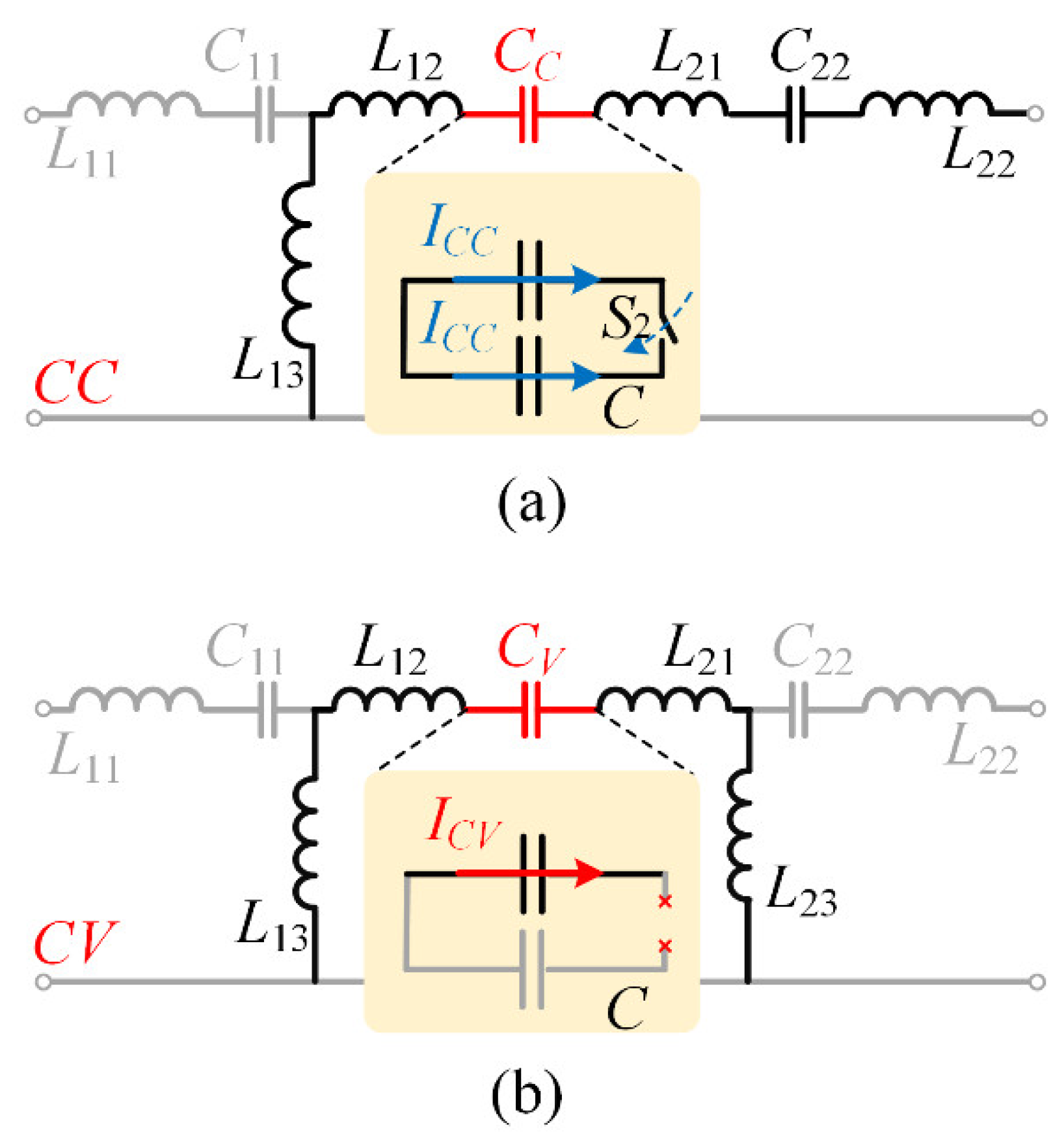
Obviously, to compensate for the impedance change caused by the topology switching in Figure 5 and to ensure that ZPA can be implemented under both CC and CV output modes, the VC is supposed to alter from one defined capacitance to another capacitance without continuous change of capacitance. Thus, for the sake of simplification, in this article, a scheme similar to a capacitor array is applied to realize capacitance hopping. The structure diagram of VC is depicted in Figure 6a in CC mode, and Figure 6b in CV mode, besides, the design method is discussed as follows:
During the CV output mode, the capacitance of VC CV can be designed as C12 and C21 in series in Figure 3 according to (1) and (21), and the capacitance is calculated as:
C V = C 12 C 21 C 12 + C 21 = 1 ( γ 12 L 13 + γ 21 L 23 ) ω 2 ,
furthermore, by substituting (26) and (29) into (30), CV can be derived as:
C V = π 2 V b I b 4 ( γ 12 V b + γ 21 V d c ) ω V d c .
While operating under the CC mode in Figure 6a, the capacitance of CC VC can be expressed by
j ( ω L 12 1 ω C C + ω L 21 + ω L 22 1 ω C 22 ) = j ω L 13 ,
meanwhile, adapting the parameter design method, CC can be defined as:
1 ω C C = α ω L 13 .
Similarly, according to (1) and (32), α can be calculated by
α = 1 + β 12 + ( β 21 1 ) L 23 L 13 .
Then, substituting (26) and (29) into (33), CC can be expressed by
C C = π 2 V b I b 4 [ V b + β 12 V b + ( β 21 1 ) V d c ] ω V d c .
Finally, the capacitance of C can be expressed by C = C C C V . The parameter design process is shown in Figure 7.
According to (21), all β parameters can be zero, which means the corresponding inductors can be removed from the DT converter. Nevertheless, by analyzing (34), the β12 and β21 cannot equal zero simultaneously in order to keep the CC bigger than zero. Therefore, the DT converter can be simplified as shown in Figure 8. These two design options are equivalent when analyzed with FHA and can be chosen based on varying application scenarios and requirements. The simplified DT circuit can be selected to meet specifications such as power density, volume, and weight. Conversely, the circuit topology that preserves inductance can be chosen for conditions that require sensitivity to high-frequency components within the resonant tank.

4. Experiment and Results

In this part, a dc-dc converter prototype equipped with the DT as the resonant converter has been built to verify the feasibility of the proposed theoretical analyses. The prototype is shown in Figure 9 and Figure 10, which is primarily composed of the following three parts: a full-bridge inverter, a DT as the resonant converter, and a full-bridge rectifier consisting of diodes. Furthermore, the inverter consists of two half-bridge MOSFETs (FF6MR12KM1P), and the MOSFETs of the AC switch S are IV1Q12750T3. The diodes of the full-bridge rectifier are CI10T60C3. In addition, the prototype is also supplied by a DC power supply (MP20020D), and an electronic load (ET5410Aplus) is used to simulate the variation of load. The oscilloscope (Tektronix MDO3024), the differential probe (RP1025D), and the current probe (RP1001C) are used to measure the waveforms in this part below. All the control algorithms including the PWM control and the AC switch control are both implemented by the controller (DSP28335). The key parameters of the DT resonant converter are shown in Table 1.

4.1. Load-Independent Experiment Results and Analysis

In order to verify the ability to contain the output current and output voltage of the experimental prototype, the load-independent experiments of CC output mode and CV output mode have been examined.

4.1.1. CC Output Mode

Due to the CC mode mainly operating under the initial stage of battery charging, when the internal resistance of the battery is low. Thus, in order to simulate this charging condition, the experimented load is set to range from 9 Ω to 50 Ω. Three sets of data are obtained by configuring the input voltage to three fixed values, 48 V, 65 V, and 96 V, then varying the load resistance.
The following is an analysis of one set of data and the results are as follows. The experimental output current fluctuates around the theoretical value of 2.104 A, furthermore, all the experimental output current values are lower than the theoretical value, which completely meets the theoretical expectations because of the conversion and switch losses. The maximum current occurs when the load is 9.2 Ω, the output current is 2.088 A, and the output voltage is 19.21 V. The maximum error occurs when the load is 48.7 Ω, the output current is 1.998 A, and the output voltage is 97.3 V.
In addition, the load-independent ability can be expressed in terms of the relative error between the experimental current value and the theoretical current value, and the closer the relative error is to zero, the greater the load-independent ability of the proposed system under the CC mode is. The relative error is depicted in Figure 11. According to Figure 11, the relative error is approximately less than 5% in the whole range of experimental load during set one in lower current value. Furthermore, as the load resistance and output current increase, there is a slight increase in relative error.

4.1.2. CV Output Mode

During the CV output mode, the resistance of the batteries commonly ranges from tens of ohms to hundreds of ohms. Therefore, the experimental load is set in the range of 40 Ω to 300 Ω, and also set the dc link voltage as three fixed values, 44 V, 72 V, and 96 V. Similarly to the CC mode, one set of data and results are analyzed as follows. With load resistance increasing from 40 Ω to 300 Ω, accordingly, the output voltage increases from 44.17 V to 46.38 V. The maximum error, which is approximately 2.21 V, occurs when the load resistance is equal to 301.24 Ω.
The load-independent ability of the CV output mode can also be expressed as the relative error between the experimental voltage and the theoretical voltage. Figure 12 depicts the relative error, with the region where the error is greater than 5% marked. As shown in Figure 12, during the whole load resistance range, the relative error is less than 8%. When the load resistance is in the range of 40 Ω to 220 Ω, the error between the experimental output voltage and the theoretical output voltage is lower than 5%. Further analysis shows that with the increase in the load resistance to 300 Ω and a large resistance nearing the end of the battery charge, the relative error increases to about 8% but decreases with the increase in input voltage.

4.2. Battery Experiment and Results

4.2.1. Performance on Electronic Loads

In this part, a battery charger prototype with 48 V output voltage and 1.56 A output current is implemented to verify the feasibility of the proposed system which adopts a DT as a resonant converter. Before the experiment, the setting of the electronic loads should be demonstrated. In CC output mode, the initial resistance of the load is set to 12 Ω and the end resistance is 32 Ω. Similarly, during the CV output mode, the load resistance altered from 32 Ω to 250 Ω.
Figure 13 shows the measured transient-state and steady-state waveforms of the input current ii and voltage ui of the DT and the output voltage ub and current ib of the rectifier, namely the charging voltage and the charging current. Obviously, during the whole charging process, in both CC and CV modes, the input current and voltage are almost in the same phase, which means the reactive power of the DT converter is substantially zero.
Figure 13a shows the transient state of the DT converter in CC output mode. In Figure 13a, the charging voltage ub increases from 20.93 V to 30.26 V, then to 47.60 V, accordingly to the load resistance increases, while the charging current ib nearly remains the same value 1.52 A. At the same time, the input voltage ui and the control variable of DT, are not changed, which indicates the DT converter can achieve CC output mode in different loads without control. Then Figure 13c shows the steady-state of the CC mode in three different loads, with increasing resistances 13.75 Ω, 20 Ω, and 31.5Ω, the phase of input current gradually lags behind the input voltage, and the switch of the inverter changes from critical-ZVS to ZVS. Therefore, the switching loss is reduced and the conversion efficiency of the CC output mode improves by degrees.
On the contrary, from Figure 13b, in CV mode, the charging voltage ub is relatively stable in different loads without altering the input voltage ui to maintain the stabilization of the output voltage ub in 48.2 V. Further, according to the steady-state waveforms in three different loads 44 Ω, 75 Ω, and 220 Ω, it is evident that the phase of input voltage ui leads slightly to that of current ii, which means the DT converter can achieve ZVS during mostly CV output mode. Additionally, with the load resistance increasing, the leading-phase angle declines to zero. Finally, the DT converter enters the critical-ZVS state. In conclusion, according to Figure 13, the DT converter can achieve CC/CV mode and ZPA at a fixed frequency and duty cycle with the parameters satisfying Equation (21) in Section 2, which will significantly reduce the circulating energy and further improve the conversion efficiency of EVs and EBs chargers.
To further evaluate the performance of the prototype charger on electronic loads, the output current versus load resistance and the output voltage versus load resistance are plotted in Figure 14, which is a description of the charging profile. Additionally, the (dc-dc) conversion efficiency and output power are also displayed in Figure 15.
From the experimental results and analysis, the output current of CC mode fluctuates slightly around 1.51 A, and the maximum relative error caused by the load variation is less than 1.1%. As for CV mode, the theoretical voltage is 48 V. The output voltage increases from 48.19 V to 50.65 V, and the relative error increases from 0.004% to 5.1% accordingly. As to Figure 16, the maximum efficiency of the prototype is up to 97.5% occurring around the maximum output power, as well as the charging efficiency is higher than 92% during the whole experimental charging process. Compared with conventional LLCs that used PFM or PS control, DT is more suitable for EVs or EBs charging scenarios, owing to its high conversion efficiency over the wide-load range.

4.2.2. Performance on Battery Pack

Before the experiment analysis, the battery pack conditions are presented as follows: the initial charge voltage of the battery cell is 2.2 V, the final charge voltage is 4.2 V, and a total of 24 battery cells are connected in series to form a battery pack. Furthermore, the theoretical charging current/voltage of CC/CV mode is 3.12 A and 96 V, respectively. In CC mode, the output voltage rises with the resistance of the battery pack. When the voltage reaches 96 V, the ACs turn on, and the variable capacitor changes, then the prototype accesses the CV mode until the charging current is less than 0.31 A (10% of the CC output current) finishing the charging process.
Similarly, the charging current and charging voltage are illustrated in Figure 16 to display the battery charging profile. Moreover, the efficiency and power are also pictured in Figure 17.
According to Figure 16 and Figure 17, and the experimental results, the charging process can be described as follows: during the CC mode, the charging current declines from 3.11 A to 2.98 A, which means a 4.18% relative error is generated in CC mode due to the increasing resistance of battery pack. Additionally, during the whole time of CC mode, the efficiency is higher than 93%, and the maximum efficiency is measured as 95.9%. Then, the prototype alters to operate in CV mode. During CV mode, the charging voltage rises from 96.69 V to 100.98 V with a 4.44% relative error caused, finally, at the same time the efficiency slowly drops from 96.7% to 89.7%. Significantly, the efficiency of the prototype is above 89% through the whole charging process, both CC and CV modes, until the current declines to the regulated end current of 0.31 A.
Based on the performance of DT on the battery pack, the proposed DT converter operating under a fixed frequency and constant duty cycle can switch the CC/CV mode depending on the state of the battery (SoC) and can maintain the current and voltage constant in CC/CV mode. Moreover, the conversion efficiency of the DT converter is relatively high in the whole charging process. Thus, EVs or EBs that deploy DT converters will improve the safety and performance of the lithium-ion battery without an additionally sophisticated control scheme.

4.3. Power Loss Analysis and Comparisons

The total power loss is divided into several parts in terms of the physical structure of the DT resonant converter in Figure 18. From Figure 18, obviously, in CC output mode when the output power is 180 W, because of the DT converter under the critical-ZVS state, there are few reactive power losses and switching losses of the converter. At this point, the VC introduces additional power losses in the CC output mode. As to CV 288 W and 30 W, it is clear that the power loss of S1 only exists in this mode, and the percentage increases with the decline of the charging current, namely output power, gradually. Besides, ZVS can be achieved in most CV output modes, resulting in low switching losses. In both CC and CV output modes, the inductor power losses are the dominant losses of the DT converters, the actual value of which is determined only by the output current and the resistance of the inductors. In reality, the resistance value of the inductor always exists. Due to the parallel structure of the converter, when the load increases, the proportion of current flowing through the converter increases, resulting in an increase in the power loss of the inductor.
Some comparisons between the proposed DT converter with different available dc-dc converters are displayed in Table 2. Based on the results, the proposed DT converter offers significant advantages in terms of the simplicity of the control scheme, high conversion efficiency in the wide-load range, and inherent load-independent characteristics. Additionally, the DT converter is highly suitable for application in wide-load conditions [15,26], especially for battery charging, due to its high conversion efficiency in the whole load range.

5. Conclusions

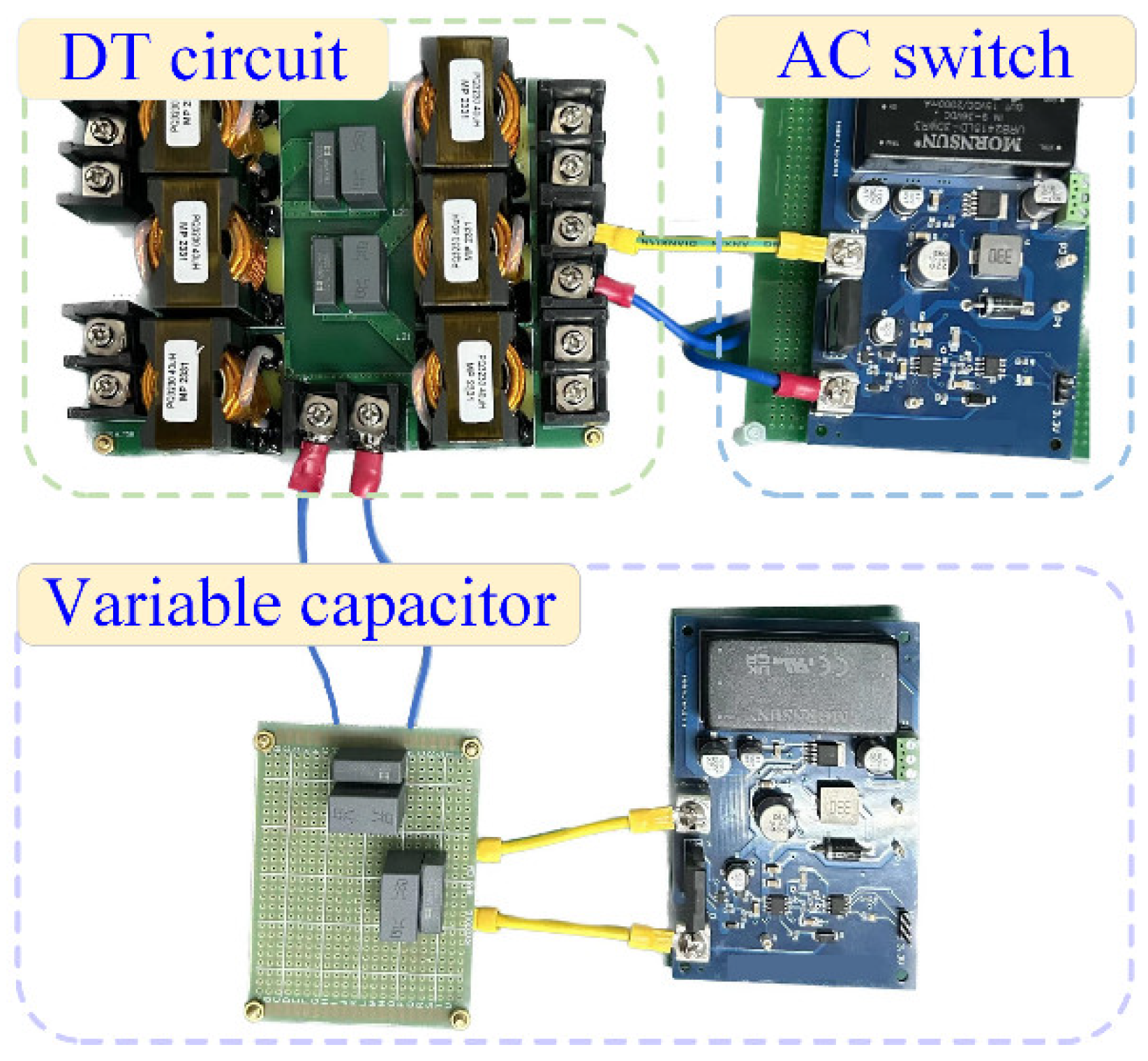
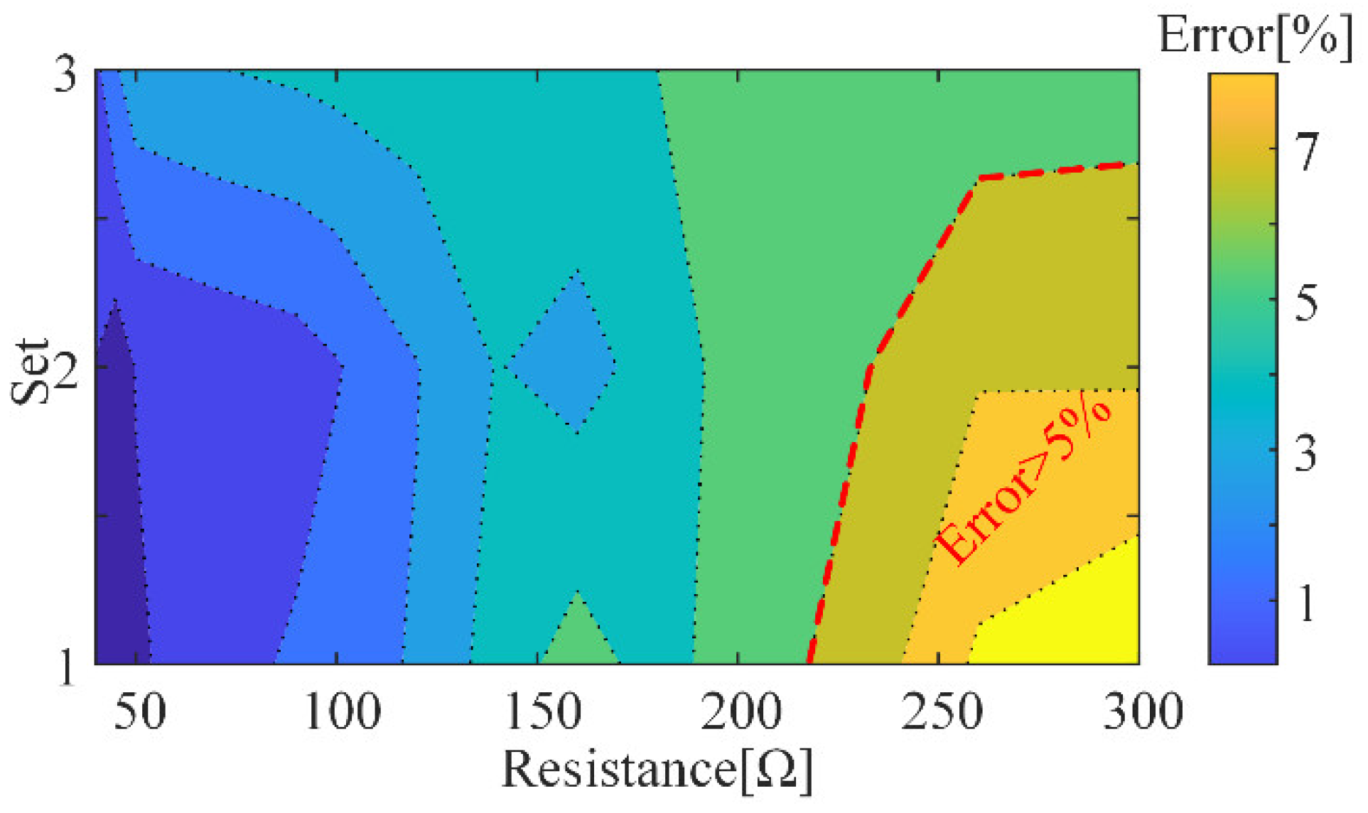
In this article, a DT with ACs and a variable capacitor are applied to the dc-dc converter for EV and EB battery chargers. The proposed DT converter can implement the switching of CC/CV to CV or CC output mode by altering the states of ACs and changing the capacitance of the variable capacitor without changing the switching frequency, which means the DT converter can operate at the resonant frequency, to significantly decrease the circulating energy and conductance loss, meanwhile, the dependence on PFC is also reduced compared with that LLC converters. Besides, the proposed DT or simplified DT (sDT) is adapted to accommodate various application scenarios. For instance, the simplified DT, with fewer inductors, is better suited for lightweight and high-power-density mobile platforms. The normal DT with the equivalent resonant state by FHA to sDT, depending on the filter inductors, can significantly enhance the filtering effect and boost output accuracy, thereby mitigating the impact of high-frequency components on the system. Furthermore, the primary switches can mostly achieve ZVS during the CC output mode and realize ZVS or critical ZVS in the whole CV output mode. Meanwhile, in the theoretical derivation of the DT, the conditions for achieving CC and CV output and system ZPA are derived, besides, a design method for parameters of the DT according to the charging current and voltage of batteries are also brought. Finally, to verify the theoretical analysis, a laboratory-scale prototype with the DT for battery charging is built. The load-independent ability and control accuracy of the DT are verified by the experiment. Additionally, the performance of the prototype on both electronic loads and a 96 V/3 A battery pack is displayed and analyzed. The experimental results demonstrate that the DT converter can operate under CC and CV output modes with less than 4.18% and 4.44% relative error, respectively, and during the whole charging process, the dc-dc conversion efficiency is higher than 89.7%, further, the maximum efficiency is measured as 96.7% in CC output mode.
The contribution of this paper can be summarized as follows. The DT resonant converter avoids the issues caused by PFM modulation and reduces the circulating current energy losses by means of the fixed frequency modulation at the resonant frequency. In addition, the gain of the output voltage is broadened by parametric design with a load-independent approach. Finally, the CC-CV charging can be realized by topology reconfiguration.

Author Contributions

Conceptualization, X.W.; methodology, Y.S.; software, S.C.; validation, S.C. investigation, Y.S.; resources, G.L.; visualization, Z.Z.; supervision, X.W.; funding acquisition, G.L. All authors have read and agreed to the published version of the manuscript.

Funding

This work was supported by the National Natural Science Foundation of China (Project No. 51977138).

Data Availability Statement

Data is contained within the article.

Conflicts of Interest

The authors declare no conflict of interest.

Abbreviations

CCConstant current
CVConstant voltage
EVsElectrical vehicles
EBsElectrical bikes
ZPAZero phase angle
ICEInternal combustion engines
PFCPower factor correction
ZVSZero voltage switching
ZCSZero current switching
PFMPulse frequency modulation
PSPhase shift
SPWMSymmetric pulse width modulation
THDTotal harmonic distortion
FHAFundamental harmonic analysis

References

  1. Rajper, S.Z.; Albrecht, J. Prospects of electric vehicles in the developing countries: A literature review. Sustainability 2020, 12, 1906. [Google Scholar] [CrossRef]
  2. Chen, K.; Zhang, Z. In-flight wireless charging: A promising application-oriented charging technique for drones. IEEE Ind. Electron. Mag. 2023, 2–12. [Google Scholar] [CrossRef]
  3. Yilmaz, M.; Krein, P.T. Review of battery charger topologies, charging power levels, and infrastructure for plug-in electric and hybrid vehicles. IEEE Trans. Power Electron. 2013, 28, 2151–2169. [Google Scholar] [CrossRef]
  4. Ehsani, M.; Gao, Y.; Gay, S.E.; Emadi, A. Modern Electric Hybrid Electric and Feal Cell Vehicles; CRC Press: Boca Raton, FL, USA, 2005. [Google Scholar]
  5. Saber, A.Y.; Venayagamoorthy, G.K. One million plug-in electric vehicles on the road by 2015. In Proceedings of the 2009 12th International IEEE Conference on Intelligent Transportation Systems, St. Louis, MO, USA, 4–7 October 2009; pp. 141–147. [Google Scholar]
  6. Bai, H.K.; Costinett, D.; Tolbert, L.M.; Qin, R.; Zhu, L.; Liang, Z.; Huang, Y. Charging Electric Vehicle Batteries: Wired and Wireless Power Transfer: Exploring EV charging technologies. IEEE Power Electron. Mag. 2022, 9, 14–29. [Google Scholar] [CrossRef]
  7. Lu, J.; Zhu, G.; Lin, D.; Zhang, Y.; Jiang, J.; Mi, C.C. Unified load-independent ZPA analysis and design in CC and CV modes of higher order resonant circuits for WPT systems. IEEE Trans. Transp. Electrif. 2019, 5, 977–987. [Google Scholar] [CrossRef]
  8. Chen, Y.; Zhang, H.; Park, S.-J.; Kim, D.-H. A switching hybrid LCC-S compensation topology for constant current/voltage EV wireless charging. IEEE Access 2019, 7, 133924–133935. [Google Scholar] [CrossRef]
  9. Wang, S.; Liu, Y.; Wang, X. Resonant Converter for Battery Charging Applications with CC/CV Output Profiles. IEEE Access 2020, 8, 54879–54886. [Google Scholar] [CrossRef]
  10. Wang, H.; Li, Z. A PWM LLC Type Resonant Converter Adapted to Wide Output Range in PEV Charging Applications. IEEE Trans. Power Electron. 2017, 33, 3791–3801. [Google Scholar] [CrossRef]
  11. Zeng, J.; Zhang, G.; Yu, S.S.; Zhang, B.; Zhang, Y. LLC resonant converter topologies and industrial applications—A review. Chin. J. Electr. Eng. 2020, 6, 73–84. [Google Scholar] [CrossRef]
  12. Cui, C.; Pehrman, D.; Liu, Y.; Zhang, Q. Zero Voltage Switching for High Power Three-Phase Inductive Power Transfer with a Dual Active Bridge. IEEE Access 2024, 12, 7121–7133. [Google Scholar] [CrossRef]
  13. Wei, Y.; Luo, Q.; Mantooth, H.A. A Novel LLC Converter with Topology Morphing Control for Wide Input Voltage Range Application. IEEE J. Emerg. Sel. Top. Power Electron. 2020, 10, 1563–1574. [Google Scholar] [CrossRef]
  14. Beiranvand, R.; Rashidian, B.; Zolghadri, M.R.; Alavi, S.M.H. A design procedure for optimizing the LLC resonant converter as a wide output range voltage source. IEEE Trans. Power Electron. 2012, 27, 3749–3763. [Google Scholar] [CrossRef]
  15. Musavi, F.; Craciun, M.; Gautam, D.S.; Eberle, W.; Dunford, W.G. An LLC resonant DC–DC converter for wide output voltage range battery charging applications. IEEE Trans. Power Electron. 2013, 28, 5437–5445. [Google Scholar] [CrossRef]
  16. McDonald, B.; Wang, F. LLC performance enhancements with frequency and phase shift modulation control. In Proceedings of the 2014 IEEE Applied Power Electronics Conference and Exposition—APEC 2014, Fort Worth, TX, USA, 16–20 March 2014; pp. 2036–2040. [Google Scholar]
  17. Pan, H.; He, C.; Ajmal, F.; Chen, H.; Chen, G. Pulse-width modulation control strategy for high efficiency LLC resonant converter with light load applications. IET Power Electron. 2014, 7, 2887–2894. [Google Scholar] [CrossRef]
  18. Park, H.P.; Jung, J.H. PWM and PFM hybrid control method for LLC resonant converters in high switching frequency operation. IEEE Trans. Ind. Electron. 2017, 64, 253–263. [Google Scholar] [CrossRef]
  19. Arazi, M.; Payman, A.; Camara, M.B.; Dakyo, B. Bidirectional Interface Resonant Converter for Wide Voltage Range Storage Applications. Sustainability 2022, 14, 377. [Google Scholar] [CrossRef]
  20. Wang, H.; Dusmez, S.; Khaligh, A. Maximum efficiency point tracking technique for LLC-based PEV chargers through variable DC link control. IEEE Trans. Ind. Electron. 2014, 61, 6041–6049. [Google Scholar] [CrossRef]
  21. Dong, Z.; Wang, D. Improved hybrid control LLC resonant converter for electric vehicle charging. In Proceedings of the 2022 IEEE 6th Advanced Information Technology, Electronic and Automation Control Conference (IAEAC), Beijing, China, 3–5 October 2022; pp. 215–219. [Google Scholar]
  22. Huau, H.; Fang, X.; Chen, F.; Shen, Z.J.; Batarseh, I. A dual-bridge LLC resonant converter with fixed-frequency PWM control for wide input applications. IEEE Trans. Power Electron. 2013, 28, 1946–1960. [Google Scholar]
  23. Vu, H.-N.; Choi, W. A Novel Dual Full-Bridge LLC Resonant Converter for CC and CV Charges of Batteries for Electric Vehicles. IEEE Trans. Ind. Electron. 2018, 65, 2212–2225. [Google Scholar] [CrossRef]
  24. Wei, Y.; Luo, Q.; Du, X.; Altin, N.; Nasiri, A.; Alonso, J.M. A Dual Half-Bridge LLC Resonant Converter with Magnetic Control for Battery Charger Application. IEEE Trans. Power Electron. 2020, 35, 2196–2207. [Google Scholar] [CrossRef]
  25. Erickson, R.W.; Maksimovic, D. Fundamentals of Power Electronics, 2nd ed.; Kluwer: Norwell, MA, USA, 2001. [Google Scholar]
  26. Li, X.; Ma, H.; Ren, S.; Yi, J.; Lu, S.; Feng, Q. A Novel LCL Resonant Converter with Inherent CC-CV Output for On-Board Chargers of Plug-In Electric Vehicles. IEEE Trans. Power Electron. 2023, 38, 4212–4217. [Google Scholar] [CrossRef]
  27. Wu, X.; Li, R.; Cai, X. A Wide Output Voltage Range LLC Resonant Converter Based on Topology Reconfiguration Method. IEEE J. Emerg. Sel. Top. Power Electron. 2022, 10, 969–983. [Google Scholar] [CrossRef]
Figure 1. Typical charging profile of lithium-ion battery.
Electronics 13 00533 g001
Figure 2. Common structure of battery chargers.
Electronics 13 00533 g002
Figure 3. Schematic of dc-dc converter with a DT.
Electronics 13 00533 g003
Figure 4. The equivalent circuit of T-circuit.
Electronics 13 00533 g004
Figure 5. The topology of DT under CC/CV mode.
Electronics 13 00533 g005
Figure 6. Structure of the variable capacitor operating under CC (a) and CV (b) modes.
Electronics 13 00533 g006
Figure 7. Parameter design flowchart.
Electronics 13 00533 g007
Figure 8. Simplified topology of DT converter.
Electronics 13 00533 g008
Figure 9. Experimental prototype.
Electronics 13 00533 g009
Figure 10. DT with ACs and VC.
Electronics 13 00533 g010
Figure 11. Relative error between the experimental current value and theoretical current.
Electronics 13 00533 g011
Figure 12. Relative error between experimental voltage value and theoretical voltage.
Electronics 13 00533 g012
Figure 13. Measured transient-state waveforms of input current ii, input voltage ui of DT, charging voltage ub, and charging current ib (a) in CC output mode, and (b) in CV output mode. That of measured steady-state waveforms (c) in CC output mode, and (d) in CV output mode.
Electronics 13 00533 g013
Figure 14. Charging profile of the prototype on electronic loads.
Electronics 13 00533 g014
Figure 15. Output power and dc-dc conversion efficiency of the prototype on electronic loads.
Electronics 13 00533 g015
Figure 16. Charging profile of the prototype on battery pack.
Electronics 13 00533 g016
Figure 17. Output power and dc-dc conversion efficiency of the prototype on battery pack.
Electronics 13 00533 g017
Figure 18. Break-up power losses of the DT converter with different output power.
Electronics 13 00533 g018
Table 1. Design Parameters of the Prototype DT converter.
ParameterDesignatorValue
L13Inductance of first T-circuit39.4 μH
L23Inductance of second T-circuit39.4 μH
fSwitching frequency100 kHz
αVariable capacitance factor2
βInductance factor1
γCapacitance factor2
CVCapacitance of VC in CV output mode15.91 nF
CCCapacitance of VC in CC output mode31.83 nF
RL13Equivalent resistance of L130.08 Ω
RL23Equivalent resistance of L230.10 Ω
RLEquivalent resistance of L0.05 Ω
Table 2. Comparisons between the Proposed DT Converter with Different Converter.
Reference[15][24][26][27]Proposed
Switching frequencyWide rangeFixedFixedMedium rangeFixed
Max. efficiency96.0%95.5%95.5%96.4%96.7%
EST.AVE. efficiency-90.8%90.5%-94.0%
CC-CVNoYesYesNoYes
Modes13242
Capacitor number12123
Inductor number24323
Control schemeYesYesNoYesNo
Disclaimer/Publisher’s Note: The statements, opinions and data contained in all publications are solely those of the individual author(s) and contributor(s) and not of MDPI and/or the editor(s). MDPI and/or the editor(s) disclaim responsibility for any injury to people or property resulting from any ideas, methods, instructions or products referred to in the content.

