Abstract
This paper proposes a new automatic design method based on continuous and binary optimization for dual-band and wideband filtering power dividers (FPDs). The designs utilize an optimization process to manipulate the multiple modes of a patch radiator. In this way, both dual-band and wideband operations can be achieved. Meanwhile, the filtering property is also taken into consideration during the optimization, which finally produces power dividers with filtering functions. The design process is highly automatic to minimize manual calculations and simulations. Finally, a dual-band filtering power divider whose center frequencies are 2.4 GHz and 6 GHz and a wideband filtering power divider operating from 3.7 GHz to 5.25 GHz are designed and fabricated for validation.
1. Introduction
In recent years, integrated design methods for a radio frequency front end (RFFE) have become a new trend to meet the demand for miniaturization and multi-functions of the system. The main idea of the integrated design is to integrate multiple RF components into one module, thus reducing the size of the system and minimizing the insertion loss between different components [1]. The popular integrated modules nowadays are filtering antenna [2,3,4], and filtering power divider [5,6]. The design of the FPDs is to integrate the filter function into the power dividers, enabling the device to realize both filtering and power dividing functions.
In the early research, the FPD was mainly designed based on the microstrip power divider. The design procedure usually requires a basic architecture of the power divider, such as the Wilkinson and Gysel divider. Then, a filtering component is inserted or coupled to the transmission lines in the power divider. In this way, the transmission matrices of power splitting are satisfied, and transmission zeroes (TZs) are also introduced to realize a dual function of the device [7,8,9]. On the other hand, the dual function can be also obtained by a multiple resonator structure [10,11,12]. These designs can further minimize the size of the power divider since they can avoid the conventional quarter-wavelength transformers in the topology.
However, although the insertion loss between the filter and power divider is successfully eliminated in the microstrip FPD, it still suffers from a relatively high conductor loss and low power dissipation capacity due to the limitation of the microstrip line’s width. Hence, some have proposed FPDs based on waveguide or substrate-integrated waveguide (SIW) [13,14,15,16,17]. Based on the cavity model, the transmission property can be easily modeled and calculated. More importantly, these designs can handle a much higher power, which makes them suitable for high-power applications, such as base stations and radars. Nevertheless, the metal waveguides have a bulky volume and are not favorable for mobile devices, while the SIW often increases the cost of fabrication due to the numerous vias required by the structure. To deal with these drawbacks while maintaining a higher power capacity compared to the microstrip FPD, a patch resonator can be utilized to achieve power splitting and filtering. In the early work, the patch resonators were mainly used to design filters. By modifying the shape of the patch and applying specific coupling schemes, multiple resonate modes during the passband along with transmission zeroes can be achieved [18,19]. In recent years, the patch resonator was found to also be able to realize a dual function of filtering and power dividing [20,21,22]. Owing to the multiple modes of a patch resonator, such designs can obtain a wideband operation or a dual-band operation [23,24].
Despite the merits of the patch FPDs, they are usually difficult to design because unlike the microstrip and waveguide FPDs, which can apply well-developed methods (e.g., microstrip model and cavity model) to analyze and predict the model, the model of a modified patch resonator is usually harder to construct. Hence, the design process may involve numerous EM simulations and frequent adjustments of the parameters, which take up considerable time and human effort. Luckily, there have been some algorithm optimization assisted design methods for microwave devices, such as antennas [25], antenna arrays [26], and filters [27], which can promisingly reduce the time and effort needed to design an FPD [28].
Therefore, this paper proposes a novel design method for the patch FPD. Based on the particle swarm optimization (PSO) and binary particle swarm optimization (BPSO), a design process that is highly automatic and customized is elaborated and presented in the paper. The key to this design method is to find a specific shape of the patch resonator so that it can introduce TZs while keeping a power dividing function. This is performed by pixelating the patch into a 2D binary matrix, then the BPSO is utilized to solve the corresponding optimization problem. To accelerate the optimization process and enhance its ability to find the optimal solution, a coarse-to-fine optimization is designed and applied in this paper. Moreover, the fitness functions are defined in a way that they can describe the desired response accurately. To validate the algorithm, a dual-band FPD and a wideband FPD are designed, respectively, using the proposed design process. It is shown that this design method is suitable for both dual-band and wideband FPD designs, and is able to significantly decrease the time and effort needed to design a patch FPD.
2. Design of the Fundamental Models
The very first step of the design is selecting a suitable topology that can be optimized to achieve the desired transmission properties. The topology must guarantee the goal of the optimization process (i.e., the dual function of filtering and power dividing) is feasible. Since the main idea of the proposed design method is to pixelate the patch resonator and try different shapes during the optimization, it is important that the fundamental models of the patch FPD exhibit transmission properties that closely approximate those of ideal FPDs. Hence, two different fundamental models are provided in this section for solving a dual-band FPD problem and a wideband FPD problem respectively, and a detailed analysis is also given.
2.1. Fundamental Model of the Dual-Band FPD
Figure 1 gives the geometries of the fundamental models for both dual-band FPD and wideband FPD. The square patch resonators are connected to the ports by 50 microstrip lines. For the dual-band FPD model shown in Figure 1a, a shorted via is added at the center of the patch along with another pair of shorted vias located at the middle of the patch. In addition, a total of three lumped resistors (, , ) are placed in the middle gap for isolation between Port 2 and Port 3. In the fundamental model, we mainly focus on the passband of the device because it is mainly dependent on the characteristics of the fundamental model, while the TZs and isolation can be later optimized. Hence, the resistors are not considered in the following results since they do not have an effect on the passband while only Port 1 is excited.
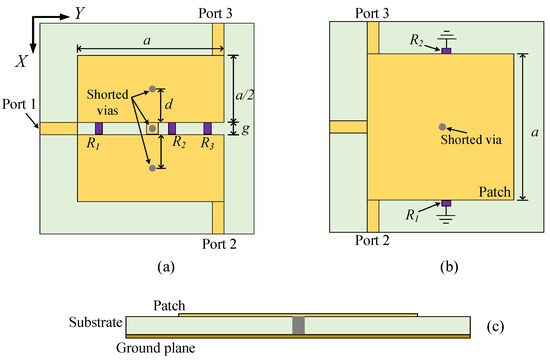
Figure 1.
Geometry of the fundamental models. (a) Dual-band FPD (top view). (b) Wideband FPD (top view). (c) Side view of the structures.
For a demonstration, the parameters of this model are given as follows: a = 28 mm, g = 0.9 mm, d = 9.1 mm, the substrate is a Rogers 4003 with a thickness of 0.305 mm, and the diameter of the vias is 1.2 mm. The simulated S-parameters result of this model is presented in Figure 2, where it can be learned that a total of six modes are excited from 1 GHz to 10 GHz. To give a further analysis, Figure 3 depicts the strength of the electric fields of these modes on the patch resonator (the microstrip feeding lines are not shown in the figure for simplicity). The theoretical E field distribution of a rectangular patch resonator can be computed by [29].
where is the strength coefficients of the TMmn mode, and L and W are the length and width of the patch. Using the above equation, certain modes of the patch resonator can be defined at the corresponding frequencies, except for mode 1, because mode 1 is generated with the aid of the shorting pins but not by the patch itself [24]. The simulated E fields shown in Figure 3 also indicate that the maximum field strength of all modes can be obtained either at the same side as the feeding port (marked as Node 1 in Figure 3a) or the diagonal location of the patch (Node 2). Hence, in order to obtain a low insertion loss of the power divider at both the lower and higher passband, the output ports (i.e., Port 2 and Port 3) must be placed near these two nodes. The locations of Port 2 and Port 3 are finally selected to be at Node 2 (and its symmetrical one) to avoid the mutual coupling between the two microstrip lines. From the transmission performance shown in Figure 2, it can be also learned that there are two modes suitable for a low-frequency passband (Mode 1 and 2) and the other four modes are more suitable to form a wider passband at the higher frequency. Therefore, this fundamental has the potential to be optimized as a dual-band filtering power divider by further modifying the shape of the patch resonator.
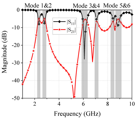
Figure 2.
Simulated and of the fundamental model for a dual-band FPD.
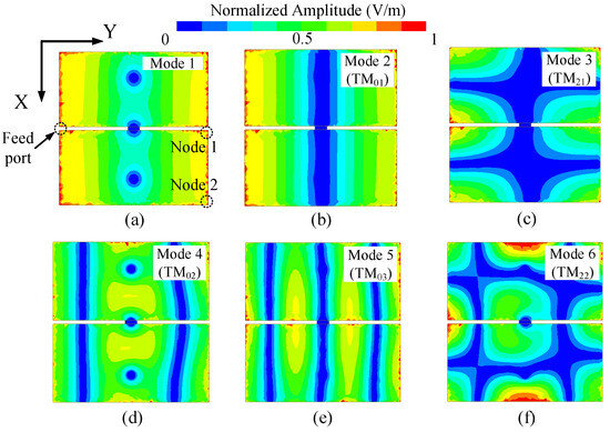
Figure 3.
Simulated electric fields of the patch resonator at different modes at (a) 2.34 GHz, (b) 2.8 GHz, (c) 6.1 GHz, (d) 7.1 GHz, (e) 8.5 GHz, and (f) 8.85 GHz.
2.2. Fundamental Model of the Wideband FPD
On the other hand, the fundamental model for a wideband FPD is simpler as illustrated in Figure 2b. Its simulated S-parameters result is presented in Figure 4. The substrate used in this model is the same as the dual-band FPD model above. For the wideband FPD model, only one shorted via is added at the center of the patch, and two lumped resistors (, ) with the same resistance are attached to the edge of the patch for good isolation. Note that the resistors are still not considered, and their values are infinite in the following simulated results since they have little effect on the modes’ frequency and patterns. In order to generate a fundamental mode (TM01) of the patch resonator at around 4.3 GHz, the size length of the patch is set to 19 mm with the same substrate as the previous model. A total of four modes are excited across 1 to 10 GHz, according to the result shown in Figure 4. Similarly, one can obtain the electric fields of these modes as shown in Figure 5. The TM′02 mode is generated because the existence of the shorted via disturbs the original TM02 mode of the patch resonator. For a single-band operation, the suppression of the higher mode is desired to obtain a better out-of-band suppression performance. Thus, Port 2 and Port 3 are placed at locations where the TM′02 mode has its minimum field strength.
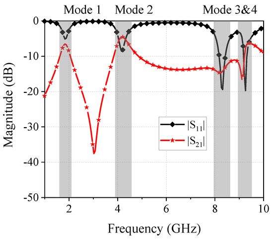
Figure 4.
Simulated and of the fundamental model for a dual-band FPD.
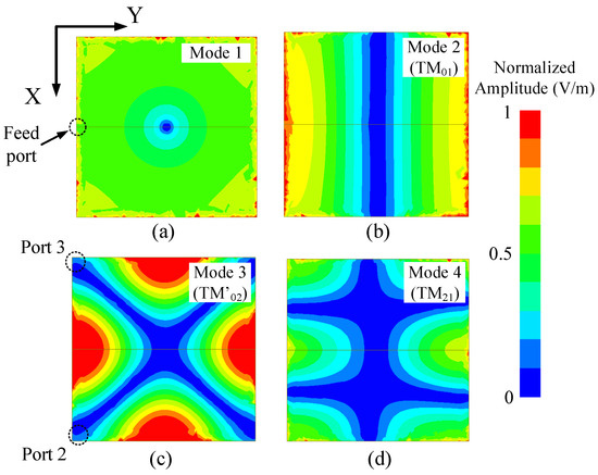
Figure 5.
Simulated electric fields of the patch resonator at different modes at (a) 2 GHz, (b) 4.1 GHz, (c) 8.3 GHz, (d) and 9.2 GHz.
3. Design of the Optimization Process
The fundamental models designed above lay the groundwork for the corresponding optimization problems. In this section, a detailed design of the optimization process is provided to effectively solve these problems. Firstly, we need to define the independent variables in the optimization problem, which also are the parameters that need to be optimized. In the specific problems of this design, the parameters are the shape of the patch resonator, the position of the resistors, and the positions of the shorted via for the dual-band FPD. Therefore, half of the patch resonator is pixelated into a 10 × 20 binary matrix, and due to the symmetry of the patch, these values can completely represent the whole patch resonator during the optimization. This procedure is illustrated in Figure 6. Note that for both dual-band and wideband FPD, the position of the center vias always remains unchanged during the whole optimization. As a result, there are 200 discrete variables for the patch resonator, 5 continuous variables for the locations of the resistors, and shorted vias (i.e., the value of d shown in Figure 1a) when solving the dual-band FPD problem. And for the wideband FPD problem, only two continuous variables are needed for the locations of the resistors.
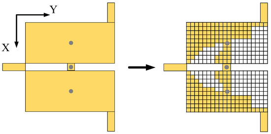
Figure 6.
Pixelation of the patch resonator.
3.1. The Modified PSO Algorithm
This paper utilizes both PSO and BPSO algorithms to solve the above problems, and they are used to solve the discrete and continuous problems, respectively. However, it is unwise to directly use the original PSO for the problems, the reasons being as follows. Firstly, the number of independent variables in this binary optimization problem is so large that it will greatly degenerate the ability of BPSO to find the global optimal solution. Secondly, the parameters of the swarm should be adaptive, as it requires a higher ability of exploration at the beginning of the process but a faster convergence is preferred at the last stage of the optimization. The fitness function should also vary with the process to describe the goals more accurately. Therefore, with the aim of speeding up the optimization process for the problem and also enhancing the ability to find the global optimal solution, a customized PSO is applied here, whose complete procedure is illustrated by the flow chart shown in Figure 7.
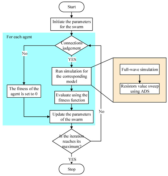
Figure 7.
Flowchart of the optimization process.
To cut down the number of variables and thus obtain higher efficiency, a coarse-to-fine optimization is applied here. The optimization process is divided into two stages: coarse optimization and fine optimization. In the coarse optimization, the patch resonator is pixelated into a 10 × 10 binary matrix instead of a 10 × 20 one, and each pixel is a rectangle with a side length ratio of 1:2, while the fine optimization divides the patch resonator further into a 10 × 20 binary matrix based on the result of the coarse optimization. At the beginning of the fine optimization, the locations of the population are imported from the individual best solution of each agent obtained in the coarse optimization. In this way, a transition from coarse optimization to fine optimization is achieved. The two stages of the optimizations share the same procedure shown in Figure 6 but use different parameters of the swarm and fitness functions.
For the BPSO algorithm, since the essence of it is to find the optimal shape of the patch, the values of the binary matrix should make its representation resemble a patch shape as closely as possible. Hence, at the beginning of the coarse optimization, the location of each agent of the population is initiated as follows:
where stands for the element at the row m, column n of the matrix for the ith agent, and is a random number generated with uniform distribution in [0, 1]. In this way, there will be more “1” in the matrices, which makes it more likely to generate a patch shape for each agent.
Before the simulation is set to obtain the result for the corresponding agent, an extra connection judgment is required here. The purpose of this procedure is to check the valid connection between the ports to prevent meaningless simulations for those models without direct connections between the ports. Figure 8 illustrates this problem with an example of a valid patch and an invalid patch, respectively. The main distinction between a valid patch and an invalid one is that the valid patch contains a direct path from Port 1 to Port 2 (or Port 3), while the invalid one does not. Hence, the transmission property of the invalid patch is bound to be poor, as the energy cannot reach the output port (i.e., Port 2 or Port 3) through the patch. Running simulations for such models is senseless since the results of them are already known. Consequently, a depth-first search (DFS) algorithm is utilized here to check the connection of the patch shape. If DFS fails to find a valid patch from Port 1 to Port 2 (or Port 3) according to the location of the agent, then the fitness of this agent is set to the worst case, which is 0 in this optimization process. This procedure can decrease the time for an iteration, especially at the beginning of the coarse optimization, where a large number of invalid patch models may be generated due to the blind searching of the initial swarm.
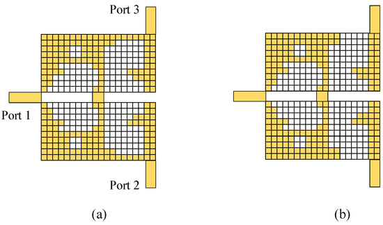
Figure 8.
Examples of the model. (a) Valid patch. (b) Invalid patch.
If the location of the agent passes the connection judgment, a script is then applied to model the patch filtering power divider according to the location and run the simulation. There are two stages of the simulation. The first stage involves a full-wave simulation for the patch FPD, which eventually produces an S-parameter result of the network without considering the resistance value of the resistors. Then the network data are proceeded by the commercial circuit simulation software Advanced Design System 2019 (ADS 2019). The ADS will perform a sweep for the resistance to find the optimal value for the resistors. This process can exclude the influence of the resistors of the FPD during the optimization process, so it enhances the ability of the algorithm to find the global optimal solution.
After the simulation, the fitness of each agent can be evaluated using the fitness function, which will be discussed in detail in the next subsection. Then, the location and velocity of each agent in both PSO and BPSO can be updated according to the results obtained in this iteration. For both PSO and BPSO, the velocity of the ith agent in the iteration is computed as:
where and are the best solutions of the ith agent and the whole group. w, , and are the weights for the influence of old velocity, the individual best location, and the group best location, respectively [30]. According to (3), a larger value of w and encourages the agent to search according to its own velocity and memory of its best location, which enhances the ability of the exploration. On the contrary, increasing will result in a better exploitation of the swarm. For the coarse optimization, we expect that the algorithm can find the position to be as close as possible to the global optimal solution, so the value of w and is relatively big to guarantee a higher ability of global searching. The fine optimization, on the other hand, requires a stronger influence of the best location of the group to increase the converge speed of the process. Hence, a larger is needed in the fine optimization.
3.2. Fitness Functions Definitions
The fitness function plays a critical role in the optimization process, as it describes the objective of the problem. There are two primary considerations when formulating the fitness function for the dual-band and wideband FPD problems in this paper. First and foremost, the fitness function must describe the dual function of filtering and power dividing accurately to guarantee that the global optimal solution found by the algorithm is the one we actually need. Secondly, the fitness function should guide the swarm toward the optimal locations. This indicates that the fitness should decrease or increase monotonically when the location deviates from the global optimum.
In this paper, the fitness function is defined based on the results of the simulation, which includes , , and . The desired transmission property of an FPD can be described in Figure 9. There are two major regions in the transmission property shown in Figure 9, namely the stopband and passband, respectively. In order to obtain a good power dividing function during the passband, one has to consider the insertion loss, the reflection coefficient, and the isolation between the two output ports. For a typical two-way power divider, an insertion loss that approaches −3 dB, a reflection coefficient lower than −10 dB, and an isolation less than −20 dB are usually desired. On the other hand, an out-of-band suppression higher than 20 dB is desired during the stopband, and the stopband should be as close to the passband as possible to guarantee a high selectivity of the FPD.
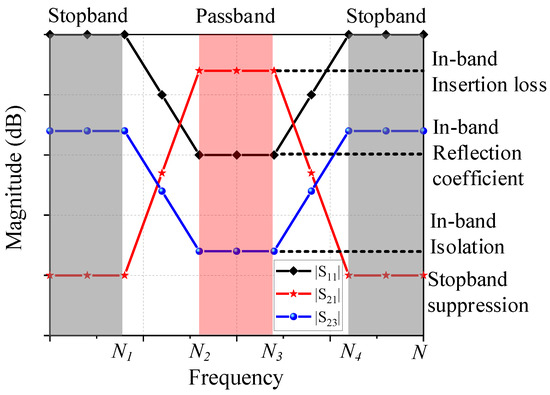
Figure 9.
Desired transmission property of an FPD.
Hence, the fitness function in this problem can be divided into three parts: the fitness of the in-band insertion loss , the fitness of the in-band isolation , and the fitness of the stopband suppression . The in-band reflection coefficient can be ignored here since a good insertion loss already implies a low reflection coefficient of the device. For the coarse optimization process, the definitions of , , and are given by:
with the limits of
Equations (4a)–(4c) consider the errors between the goal values of insertion loss, isolation, stopband (i.e., , , and ) and their corresponding simulated results. During the stopbands and passband, the equations sum up the errors at each frequency point j as the fitness. The () stands for the beginning or ending indices of the corresponding bands as shown in Figure 8. In the coarse optimization, the algorithm should find a patch shape whose transmission property is proximate to the goals. Therefore, the fitness of insertion loss and isolation vary with the errors exponentially to guarantee an in-band performance that approaches the goals. The total fitness is the weighted sum of (4a)–(4c), which can be expressed as:
where , , and are the weight for , , and , respectively. From the definitions above, one can notice that a model with a very low transmission amplitude from port to port can obtain good fitness since the isolation of the ports is high, according to (4b). This condition can occur when the resonant frequency of the patch deviates from the desired passband. To avoid such models, the weight for the isolation is non-zero only when the fitness of the in-band insertion loss reaches a specific value. This configuration prioritizes a high transmission amplitude of the FPD to ensure that the patch resonates at the desired frequency.
For the fine optimization, the definitions of the individual fitness functions , , and follow the sequence described in Algorithm 1. In contrast to the calculation in the coarse optimization given by Equations (4a)–(4c), this algorithm counts the total number of the frequency points that exactly satisfy the corresponding goal. Because, as the last stage of the optimization, we hope that the designed FPD can reach the design goals at each frequency point. After individual fitness is obtained through Algorithm 1, the total fitness of the agent is still the weighted sum of , , and , which is already defined by Equation (6).
| Algorithm 1 Fitness function for fine optimization. |
| Input: Simulated , of the agent Output: fitness of the agent:
|
4. Validation Results and Discussion
The whole optimization process including the calculation, the full-wave simulation, and the circuit simulation is executed on a workstation with an Intel Xeon Gold 5117 processor and 128 GB of RAM. For both dual-band FPD and wideband FPD models, each full-wave simulation only takes less than 5 min. To further accelerate the process, the simulation tasks are solved in parallel. A maximum of four simulations can run simultaneously on the platform.
4.1. Run Results of the Optimization Process
The algorithms use the fundamental models given in Figure 1. For the dual-band FPD, the ultimate desired operating center frequencies are 2.4 GHz and 6 GHz with a bandwidth of 0.5 GHz and 1 GHz, respectively. The population of the swarm is 44, which means a total of 44 sets of parameters are evaluated in one iteration of the algorithm.
Figure 10 gives the run results for the dual-band FPD optimization, including the fitness curves and the simulated results of the best model. The maximum iterations are 80 and 100, respectively, for the coarse optimization and the fine optimization. The fitness of the best model obtained in the coarse optimization is 330.6 after 66 iterations of the algorithm as shown in Figure 10a. Note that an upsurge can be observed after the 39th iteration because the agents have found the solution whose weight for the isolation becomes non-zero, which greatly increases the best fitness of the swarm. Figure 10b demonstrates the simulated S-parameters of the best solution in the coarse optimization. It can be learned from the figure that despite the insertion loss being high, a dual-band operation is achieved, and a roll-off can be also observed outside the passband. Based on the individual best location found in the coarse optimization, a fine optimization is then utilized to further divide the patch resonator to obtain a better result of the FPD. Figure 10c shows the fitness curve of the fine optimization. Owing to the imported initial locations, the agents do not have to search blindly at the beginning of the process, which results in higher fitness at the first iteration. The simulated results of the best solution found in the fine optimization are depicted in Figure 10d. Compared to the results shown in Figure 10b, the ultimate model has lower insertion loss, lower reflection coefficient, better selectivity, and better isolation. Hence, the final model found in this algorithm successfully realizes a dual function of filtering and power dividing at both 2.4 GHz and 6 GHz.
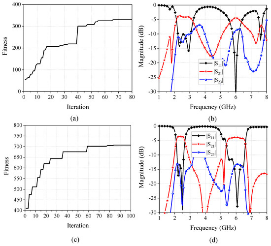
Figure 10.
Optimization results of the dual-band FPD. (a) Fitness curves of the coarse optimization. (b) Simulated results of the best model. (c) Fitness curves of the fine optimization. (d) Simulated results of the ultimate models.
Similarly, the run results for the wideband FPD are also given in Figure 11. The desired operating frequency is set to 3.7 GHz to 5.1 GHz. The fitness curve given in Figure 11a shows that the algorithm converges at the 51st iteration, with a maximum fitness of 384.8. The fitness leaps from 170 to 302.5 at the 32nd iteration, indicating that a solution with good isolation was found as proved in the simulated results given by Figure 11b. However, the fine optimization on the wideband FPD model has a more limited effect compared to the dual-band FPD. From the fitness curve shown in Figure 11c, the algorithm converges at the 65th iteration with less improvement of the best fitness. While the ultimate model exhibits improved insertion loss and selectivity compared to the results achieved in the coarse optimization, it is noteworthy that the FPD has only two TZs, inducing a poor filtering function. To further enhance the filtering performance of the wideband FPD, a pair of open stubs is placed at the output ports to provide two extra TZs. The final wideband FPD with the open stubs along with its optimized results are shown in Figure 12. With the aid of the open stubs, a total of five TZs and an out-of-band suppression of −20 dB across 2 GHz to 9 GHz can be obtained.
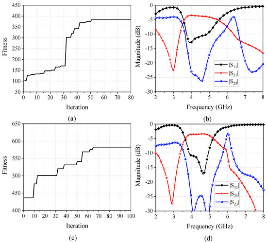
Figure 11.
Optimization results of the wideband FPD. (a) Fitness curves of the coarse optimization. (b) Simulated results of the best model. (c) Fitness curves of the fine optimization. (d) Simulated results of the ultimate models.
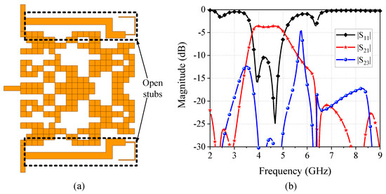
Figure 12.
Optimized wideband FPD with open stubs. (a) Structure. (b) Simulated results.
4.2. Fabrication and Measured Results
To further validate the optimized designs, prototypes for both dual-band FPD and wideband FPD are fabricated by a standard double-sided PCB process. Before the fabrication, a post-process is implemented on the pixels. As shown in Figure 13a, the diagonal pixels are connected by a single virtual point in the simulation model, which is not feasible in actual fabrication. Hence, a circular copper element is added at the junction of every two diagonally positioned pixels of the original model as illustrated by Figure 13b.
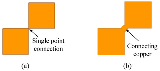
Figure 13.
Connection of the diagonal pixels with (a) single-point connection. (b) Connecting copper.
Photographs of the fabricated dual-band FPD and wideband FPD are shown in Figure 14. The lumped resistors are all in 0603 package. For the wideband FPD, the resistors are placed at the bottom layer. Two vias are used to connect the resistors and the patch resonator at the top layer as shown in Figure 14b. Note that this configuration can enable a higher power-handling ability of the power divider since the resistors are connected to the ground directly [31]. The total patch area of the dual-band FPD is 28 mm × 28.9 mm (0.65 × 0.68, is the guided wavelength at the center frequency). The size of the wideband FPD is 21.2 mm × 17.1 mm (0.52 × 0.42), including the open stubs.
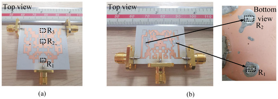
Figure 14.
Fabricated prototype of (a) dual-band FPD with R1 = R2 = 45 Ohm, R3 = 85 Ohm. (b) Wideband FPD with R1 = R2 = 50 Ohm.
The measured results of the prototypes are demonstrated and compared with the simulated ones in Figure 15. It can be learned from the figure that all experimental results are in good agreement with the simulated results. For the dual-band FPD, the center operating frequencies are 2.4 GHz and 6 GHz, with a measured 3 dB bandwidth of 0.65 GHz and 1.25 GHz, respectively. The measured maximum insertion loss is 4.05 dB during the lower passband and 4.3 dB during the upper passband, which is about 0.3 dB lower than the simulated results. A total of 6 TZs can be observed across 1 GHz to 10 GHz, which enables high selectivity of the FPD.
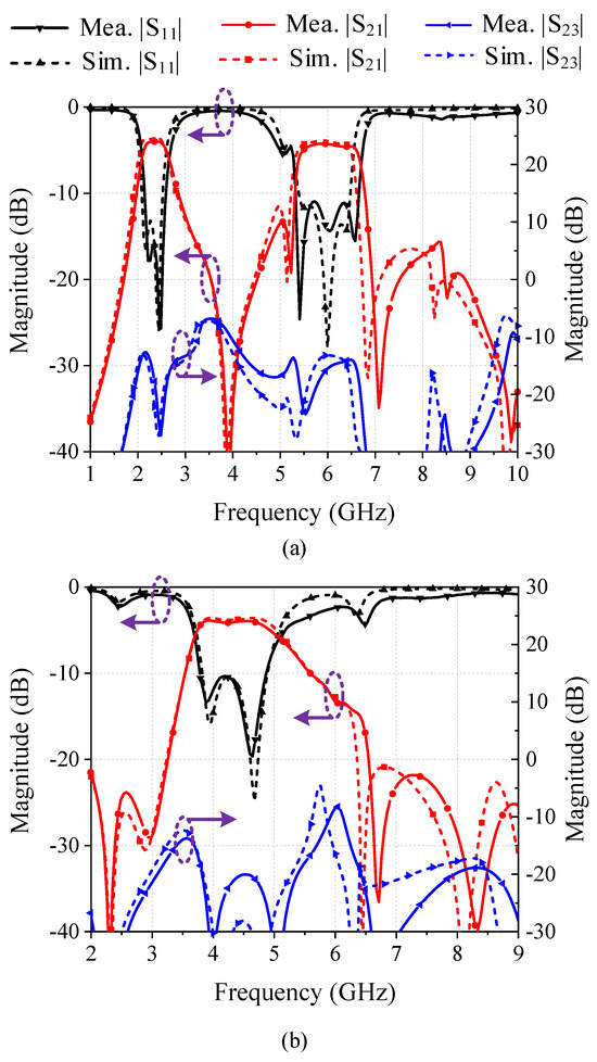
Figure 15.
Measured and simulated results of the designs. (a) Dual-band FPD. (b) Wideband FPD.
Regarding the wideband FPD, its operational frequency spans from 3.7 GHz to 5.25 GHz, with a maximum in-band insertion loss of −4.1 dB in measurement and −3.8 dB in simulation. The isolation between two output ports has a minimum value of less than −30 dB in both the measured and simulated results. Furthermore, the FPD has an out-of-band suppression higher than −20 dB, indicating an excellent noise-filtering capability.
4.3. Comparison
Table 1 and Table 2 give the comparisons of the dual-band and wideband FPD designed by this work and other reported FPDs, respectively. Note that the insertion loss in both tables does not contain the inherent 3 dB value of a two-way power divider and is the maximum value. It can be learned from Table 1 that the dual-band FPD designed by the proposed algorithm has the widest bandwidths at both operating bands. The designed dual-band FPD also has the greatest number of TZs among these works, which indicates a better selectivity as the aspect of the filter performance. On the other hand, the performance of the wideband FPD is compared in Table 2. This comparison result shows a low insertion loss of the design, and it has the widest operating bandwidth when compared to other FPDs based on the patch resonator. More importantly, both the dual-band FPD and the wideband FPD proposed in this paper are designed by a highly automatic process, which involves much less human effort and is highly customized.

Table 1.
Comparisons of the performance between the designed dual-band FPD and other works.
Table 2.
Comparisons of the performance between the designed wideband FPD and other works.
5. Conclusions
This study presents an automatic design methodology for the patch filtering power divider. Using PSO and BPSO, the optimization process proposed in this paper successfully yielded dual-band and wideband operations for the FPDs, which can minimize the human effort and manual simulations required in an FPD design. Additionally, the design goals can be completely customized by the designer, indicating that the design method can be applied in various applications. By defining proper fundamental models and the fitness function for the FPDs, good solutions can be obtained after multiple iterations of the algorithm. In addition, to further improve the efficiency of the optimization process, this paper applies a modified PSO to solve the corresponding problems, including a coarse-to-fine optimization, the path judgment using DFS, and various fitness functions. Both the simulated results and measured results demonstrate that the FPDs designed by the algorithm achieved the dual function of filtering and power dividing efficiently.
Author Contributions
Conceptualization, Z.D., K.W. and X.R.; methodology, Z.D., K.W. and X.R.; software, Z.D. and X.R.; validation, Z.D. and G.S.; formal analysis, Z.D. and K.W.; investigation, Z.D. and K.W.; resources, K.W. and X.R.; data curation, Z.D. and K.W.; writing—original draft prseparation, Z.D.; writing—review and editing, Z.D. and K.W.; visualization, Z.D. and K.W.; supervision, K.W.; project administration, K.W.; funding acquisition, K.W. All authors have read and agreed to the published version of the manuscript.
Funding
This work was supported in part by the National Key Research and Development Program of China (No. 2020YFB1807300), the National Natural Science Foundation of China under Grand 62001140, the Shenzhen Science and Technology Program under Grant KQTD20210811090116029, the Shenzhen Basic Research Program under Grant GXWD20201230155427003-20200824201212001, the Open Research Project of Guangdong Provincial Key Laboratory of Millimeter-Wave and Terahertz (No. 2019B030301002KF2002) and the Municipal Government of Quzhou under Grant No. 2022D021 and No. 2023D010.
Data Availability Statement
The source code of the algorithm can be found in the author’s GitHub page: https://github.com/ZicoDu after the article is accepted.
Conflicts of Interest
The authors declare no conflicts of interest.
References
- Mao, C.X.; Zhang, Y.; Zhang, X.Y.; Xiao, P.; Wang, Y.; Gao, S. Filtering antennas: Design methods and recent developments. IEEE Microw. Mag. 2021, 22, 52–63. [Google Scholar] [CrossRef]
- Jin, J.Y.; Liao, S.; Xue, Q. Design of filtering-radiating patch antennas with tunable radiation nulls for high selectivity. IEEE Trans. Antennas Propag. 2018, 66, 2125–2130. [Google Scholar] [CrossRef]
- Cheng, G.S.; Zhou, J.; Huang, B.Q.; Yang, L.X.; Huang, Z.X. Compact low-profile wideband filtering an-tenna without additional filtering structure. IEEE Antennas Wirel. Propag. Lett. 2023, in press.
- Hu, H.T.; Chan, C.H. Substrate-integrated-waveguide-fed wideband filtering antenna for millimeter-wave applications. IEEE Trans. Antennas Propag. 2021, 69, 8125–8135. [Google Scholar] [CrossRef]
- Sajadi, A.; Sheikhi, A.; Abdipour, A.A. simulation, and implementation of dual-band filtering power divider based on terminated coupled lines. IEEE Trans. Circuits Syst. II Express Briefs 2020, 67, 2487–2491. [Google Scholar] [CrossRef]
- Wen, P.; Ma, Z.W.; Liu, H.W.; Zhu, S.S.; Ren, B.P.; Song, Y.; Wang, X.L.; Ohira, M. Dual-band filtering power divider using dual-resonance resonators with ultrawide stopband and good isolation. IEEE Microw. Wirel. Compon. Lett. 2019, 29, 101–103. [Google Scholar] [CrossRef]
- Deng, P.H.; Dai, L.C. Unequal Wilkinson power dividers with favorable selectivity and high-isolation using coupled-line filter transformers. IEEE Trans. Microw. Theory Tech. 2012, 60, 1520–1529. [Google Scholar] [CrossRef]
- Li, Y.C.; Xue, Q.; Zhang, X.Y. Single-and dual-band power dividers integrated with bandpass filters. IEEE Trans. Microw. Theory Tech. 2012, 61, 69–76. [Google Scholar] [CrossRef]
- Wang, K.X.; Zhang, X.Y.; Hu, B.J. Gysel power divider with arbitrary power ratios and filtering responses using coupling structure. IEEE Trans. Microw. Theory Tech. 2014, 62, 431–440. [Google Scholar] [CrossRef]
- Cheong, P.; Lai, K.I.; Tam, K.W. Compact Wilkinson power divider with simultaneous bandpass response and harmonic suppression. In Proceedings of the 2010 IEEE MTT-S International Microwave Symposium, Anaheim, CA, USA, 24 May 2010. [Google Scholar]
- Luo, M.; Xu, X.; Tang, X.H.; Zhang, Y.H. A Compact Balanced-to-Balanced Filtering Gysel Power Divider Using λg/2 Resonators and Short-Stub-Loaded Resonator. IEEE Microw. Wirel. Compon. Lett. 2017, 27, 645–647. [Google Scholar] [CrossRef]
- Zhang, G.; Wang, X.; Yang, J. Dual-band microstrip filtering power divider based on one single multimode resonator. IEEE Microw. Wirel. Compon. Lett. 2018, 28, 891–893. [Google Scholar] [CrossRef]
- Mohammed, A.M.; Wang, Y. Four-way waveguide power dividers with integrated filtering function. In Proceedings of the 2015 European Microwave Conference (EuMC), Paris, France, 8 September 2015. [Google Scholar]
- Liu, B.G.; Lyu, Y.P.; Zhu, L. Compact square substrate integrated waveguide filtering power divider with wideband isolation. IEEE Microw. Wirel. Compon. Lett. 2020, 31, 109–112. [Google Scholar] [CrossRef]
- Chi, P.L.; Chen, Y.M.; Yang, T. Single-layer dual-band balanced substrate-integrated waveguide filtering power divider for 5G millimeter-wave applications. IEEE Microw. Wirel. Compon. Lett. 2020, 30, 585–588. [Google Scholar] [CrossRef]
- Pradhan, N.C.; Subramanian, K.S.; Barik, R.K.; Cheng, Q.S. Design of compact substrate integrated wave-guide based triple-and quad-band power dividers. IEEE Microw. Wirel. Compon. Lett. 2021, 31, 365–368. [Google Scholar] [CrossRef]
- Barik, R.K.; Cheng, Q.S.; Pradhan, N.C.; Sholampettai, S.K. A Compact SIW Power Divider for Dual-Band Applications. Radioengineering 2020, 29, 94–100. [Google Scholar] [CrossRef]
- Zhu, L.; Tan, B.C.; Quek, S.J. Miniaturized dual-mode bandpass filter using inductively loaded cross-slotted patch resonator. IEEE Microw. Wirel. Compon. Lett. 2005, 15, 22–24. [Google Scholar]
- Hong, J.S.; Li, S. Theory and experiment of dual-mode microstrip triangular patch resonators and filters. IEEE Trans. Microw. Theory Tech. 2004, 52, 1237–1243. [Google Scholar] [CrossRef]
- Liu, Q.; Wang, J.; Zhu, L.; Zhang, G.; Wu, W. Design of a new balanced-to-balanced filtering power divider based on square patch resonator. IEEE Trans. Microw. Theory Tech. 2018, 66, 5280–5289. [Google Scholar] [CrossRef]
- Liu, Q.; Wang, J.; Zhu, L.; Wu, W. Design of balanced-to-balanced filtering power divider with arbitrary power division ratio based on circular patch resonator. IET Microw. Antennas Propag. 2020, 14, 253–259. [Google Scholar] [CrossRef]
- Liu, Y.; Sun, S.; Yu, X.; Wu, Y.L.; Liu, Y.N. Design of a wideband filtering power divider with good in-band and out-of-band isolations. IEEE Trans. Compon. Packag. Manuf. Technol. 2019, 29, e21728. [Google Scholar] [CrossRef]
- Liu, Z.; Zhang, Q.; Liu, J.; Sun, Q.; Zhang, G.; Tang, W. A New Wideband Filtering Power Divider Based on Rectangle Patch Resonator With Compact Size. In Proceedings of the 2021 IEEE MTT-S International Microwave Workshop Series on Advanced Materials and Processes for RF and THz Applications (IMWS-AMP), Chongqing, China, 16 November 2021. [Google Scholar]
- Zhang, Q.; Zhang, G.; Liu, Z.; Chen, W.; Tang, W. Dual-band filtering power divider based on a single circular patch resonator with improved bandwidths and good isolation. IEEE Trans. Circuits Syst. II Express Briefs 2021, 68, 3411–3415. [Google Scholar] [CrossRef]
- Villegas, F.J.; Cwik, T.; Rahmat-Samii, Y.; Manteghi, M. A parallel electromagnetic genetic-algorithm optimization (EGO) application for patch antenna design. IEEE Trans. Antennas Propag. 2004, 52, 2424–2435. [Google Scholar] [CrossRef]
- Cen, L.; Yu, Z.L.; Ser, W.; Cen, W. Linear aperiodic array synthesis using an improved genetic algorithm. IEEE Trans. Antennas Propag. 2011, 60, 895–902. [Google Scholar] [CrossRef]
- Ruan, X.; Chan, C.H. Free-Form Filters Designed Using Binary Optimization Algorithm. IEEE Trans. Compon. Packag. Manuf. Technol. 2023, in press. [CrossRef]
- Chen, W.; Zhang, G.; Liu, S.C.; Yang, J.Q. Synthesis of multi-port filtering power divider for mixed topology using matrix optimization. IEEE Trans. Circuits Syst. II Express Briefs 2020, 68, 176–180. [Google Scholar] [CrossRef]
- Garg, R. Microstrip Antenna Design Handbook; Artech House: Norwood, MA, USA, 2001. [Google Scholar]
- Robinson, J.; Rahmat-Samii, Y. Particle swarm optimization in electromagnetics. IEEE Trans. Antennas Propag. 2004, 52, 397–407. [Google Scholar] [CrossRef]
- Gysel, U.H. A new N-way power divider/combiner suitable for high-power applications. In Proceedings of the 1975 IEEE-MTT-S International Microwave Symposium, Palo Alto, CA, USA, 12 May 1975. [Google Scholar]
Disclaimer/Publisher’s Note: The statements, opinions and data contained in all publications are solely those of the individual author(s) and contributor(s) and not of MDPI and/or the editor(s). MDPI and/or the editor(s) disclaim responsibility for any injury to people or property resulting from any ideas, methods, instructions or products referred to in the content. |
© 2024 by the authors. Licensee MDPI, Basel, Switzerland. This article is an open access article distributed under the terms and conditions of the Creative Commons Attribution (CC BY) license (https://creativecommons.org/licenses/by/4.0/).