Abstract
Zero-voltage zero-current switching (ZVZCS) phase-shifted full-bridge (PSFB) converters have been widely used in high-power applications because of their high efficiency, low price, and easy control. Currently, the biggest problem with PSFB converters in operation is their high duty cycle loss. With the increase in current, duty cycle loss grows and degrades their performance. Focusing on this problem, a new ZVZCS PSFB converter is proposed in this paper. This topology adds an auxiliary circuit to minimize duty cycle loss. Moreover, the lagging-leg switches can obtain zero-current switching (ZCS) easily with the help of the circuit. The auxiliary circuit is built of four metal-oxide-semiconductor field-effect transistors (MOSFETs) and an auxiliary transformer, and extra voltage can be added to the primary coils when the direct-current (DC) voltage is small. This paper discusses its operation principles and characteristics, and an experiment of a 2 kW prototype was conducted, the results of which demonstrate the advantages of the presented circuits.
1. Introduction
The application of electric vehicles has become a reality with the rapid development of lithium battery technology. The battery is a core component in electric vehicle (EV) systems, and questions of how to shorten the charging time and prolong battery life are still bottlenecks in EV systems. As such, developing a charger with high performance over a wide range is a hot issue in power electronic research fields. Nowadays, LLC (resonant converter) and PSFB converters are popular typologies for battery chargers. The LLC converter features high efficiency and no reverse recovery problem of rectifier diodes, which are popular in low- and medium-power applications [1,2,3]. But the output range is narrow due to the limited switching frequency range and flattened voltage gain, meaning this is not the best choice for the battery charger. PSFB converters, meanwhile, can adjust the output and achieve soft-switching over a wide load range, meaning they may be more suitable for a lithium battery charger. However, PSFB converters still have drawbacks that cannot be ignored, such as the narrow soft-switching range of the lagging-leg switches and a high duty cycle loss. Recently, many studies have focused on these topics, seeking to enhance the performance of PSFB converters [4,5,6,7,8].
The circuits in [9,10] utilize high primary inductance to enlarge the load range of lagging-leg switches in order to realize zero-voltage switching (ZVS). In [9], a coupled inductor with a three-winding transformer provides more resonance energy and ensures the realization of ZVS in lagging-leg switches. It can also decrease the voltage spikes of the rectifier diodes. Reference [10] proposes a new rectifier structure with five diodes, which uses two transformers and two split capacitors on the primary side. This circuit achieves a high voltage gain as well as high efficiency. But the structures in [9,10] are a little complex and may cause extra power loss during the conduction period as well as duty cycle loss. In [11,12], the realization of a better ZVS performance and less duty cycle loss relies on two diodes conducting the primary current during free-wheeling periods. With the combination of a resonant half-bridge and pulse-width modulation (PWM), the circuit in [13] can eliminate the free-wheeling current and enlarge the soft-switching load range. The auxiliary transformer in [14] decreases the current through clamping diodes and has similar soft-switching characteristics to [12]. Reference [15] utilizes two transformers to help the soft condition of the primary switches, which feature low conduction and duty cycle loss. Two LC networks cross-connect with two input-series–output-parallel PSFB modules, which permit high DC link voltage and guarantee high efficiency over a wide load range [16]. Furthermore, an improved control scheme that has been proposed can reduce the power loss caused by a circulating current by adjusting the phase shift angle [17]. In 2006, reference [18] proposed a new PSFB with a minimum circulating current. Reference [19] focuses on the hard-switching condition and the cycling current. The circuit uses a sharing bridge leg in the primary side and a hybrid rectifier in the secondary side. Moreover, the circuit has different operation modes under different load conditions. It uses a blocking capacitor to limit the cycling current and realizes ZVS of all the switches; thus, efficiency can be improved. There are two transformers in this circuit, and the design requirements of the transformers are relatively high because of the different working modes [20].
Compared with ZVS PSFB converters, zero-voltage and zero-current switching (ZVZCS) PSFB converters can avoid some inherent defects and thus have seen wide application in high-power fields [21,22,23,24]. In [23], the ripple voltage provided by a blocking capacitor is used to reset the primary current, and the reverse current is prevented by a two-diode series connecting to the lagging-leg switches. Then, a good soft-switching characteristic over a wide load range can be achieved in the lagging-leg switches. Furthermore, this circuit has minimum duty cycle loss as well as conduction loss. To better reset the primary current during the free-wheeling period, the circuit in [24] adds a clamping diode and a MOSFET behind the rectifier diodes. A controllable voltage source is used in [25] to help quickly reset the primary current, which exceeds the power rating limitation of the conventional ZVZCS converter. In [26], a wide load range of soft-switching is realized in a new topology, combining a half-bridge LLC and PSFB. Furthermore, this converter also features minimum duty cycle loss.
Duty cycle loss has a great impact on power transformation. The center-tapped clamp helps with resetting the primary current and the zero-current switching (ZCS) of the lagging-leg switches. In addition, the circuit can also reduce duty cycle loss and conduction loss [27]. In [28], the saturable inductor is substituted with two diodes; thus, the reverse current of the primary side can be prevented. The power loss caused by conduction and duty cycle loss can also be reduced. The circuit in [29] uses a snubber with capacitors and diodes to ensure the reset of the primary current. It also results in a decrease in both duty cycle loss and circulating loss. Reference [30] uses a variable saturation inductor and a near-ideal transformer. The energy in controllable inductance can ensure a wide soft-switching range and reduce conduction loss, and the small leakage inductor of the transformer can eliminate the duty cycle loss.
Recent studies have improved the applicability of PSFB. However, some problems still exist. For example, high duty cycle loss still occurs under low-input-voltage conditions, and the ratio of the transformer is difficult to optimize. This paper proposes the new topology of a ZVZCS PSFB converter, which inserts a variable voltage source in the primary side to minimize duty cycle loss. Section 2 introduces the operation principles, and an analysis is provided of technical aspects in Section 3. In Section 4, an experiment of a 2 kW prototype is reported, with results that demonstrate the performance of the converter; finally, Section 5 presents our conclusions.
2. Circuits and Operation Principles
2.1. Circuit Configuration
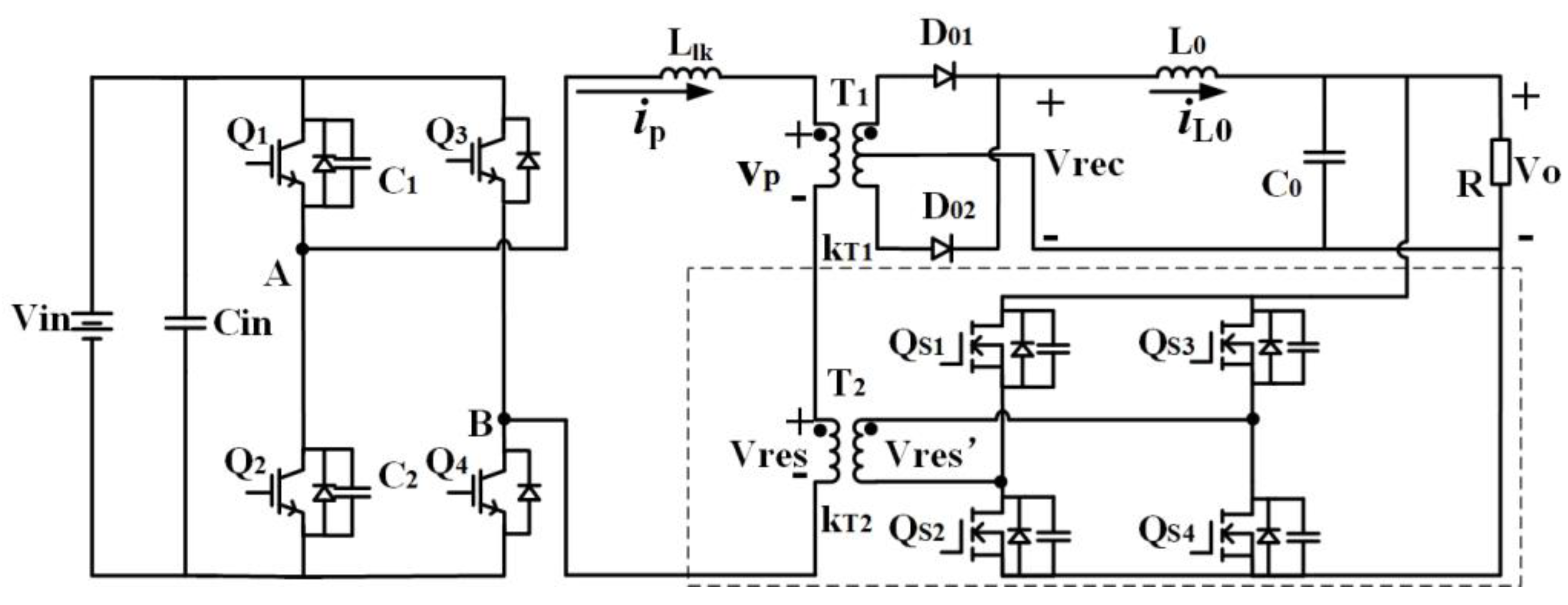
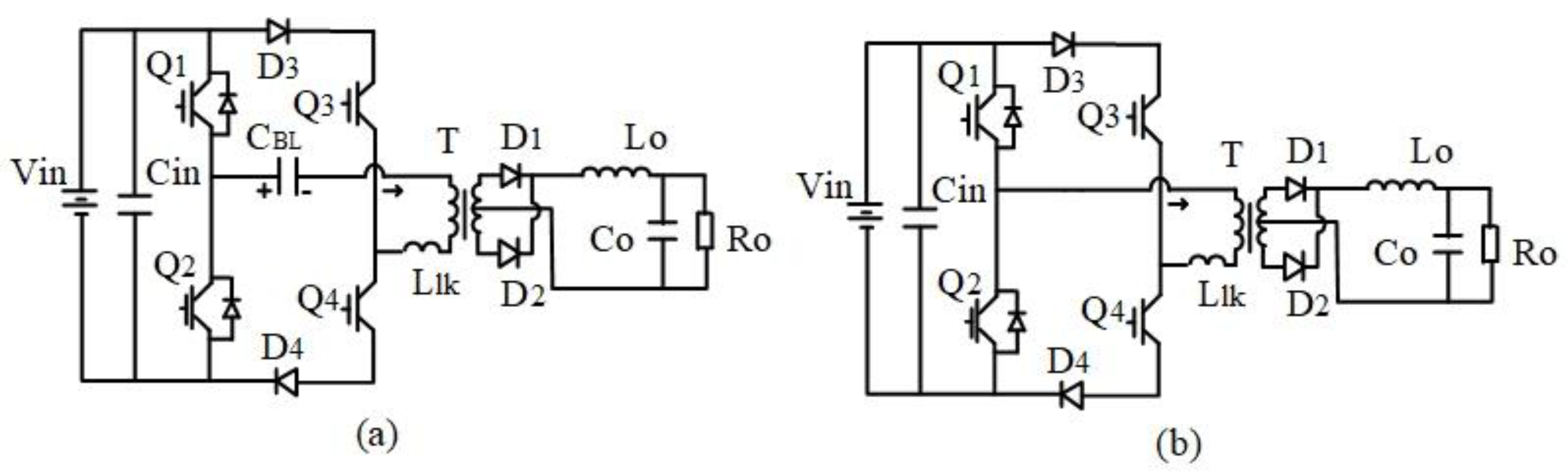
The proposed circuit, depicted in Figure 1, incorporates IGBT and MOSFET switches. Cin represents the input capacitor, with Q1 and Q2 forming the leading legs and Q3 and Q4 constituting the lagging legs. C1 and C2 denote the parasite capacitors associated with Q1 and Q2. The body diodes of Q1–Q4 are represented by D1–D4. The primary current of the main circuit is denoted as ip, and vp signifies the primary voltage. T1, the main transformer, possesses a turns ratio denoted as kT1. The auxiliary circuit comprises QS1~QS4 and T2, where T2, the reset transformer, is characterized by a turns ratio of kT2. QS1–QS4 collectively form the auxiliary bridges, and DS1–DS4 represent their respective body diodes. CS1–CS4 are the body capacitors. The primary voltage of T2 is labeled as vres’, while vres designates the secondary side voltage of the reset transformer. Llk stands for the leakage inductance of T1, and Lo represents the output inductor. To streamline the illustration, only pertinent portions of parasitic capacitances and diodes are featured in the figures. DO1 and DO2 signify the rectifier diodes.

Figure 1.
Proposed DC/DC converter.
The converter employs the auxiliary circuit to introduce a variable voltage into the primary side. During power transfer stages, this voltage remains zero, with no impact on the operation. However, during free-wheeling stages, this voltage aids in resetting the primary current, ensuring ZCS of the lagging-leg switches and effectively reducing duty cycle losses.
To simplify the analysis, it is assumed that all the components are ideal. T1 and T2 are ideal transformers with a specified turns ratio. The leakage inductance is constant. The magnetizing current of T1 and T2 is low enough to ignore. The parasitic components of Q1, Q2, Q3, and Q4 are of the same value, and iLo in this circuit can be regarded as a constant current source.
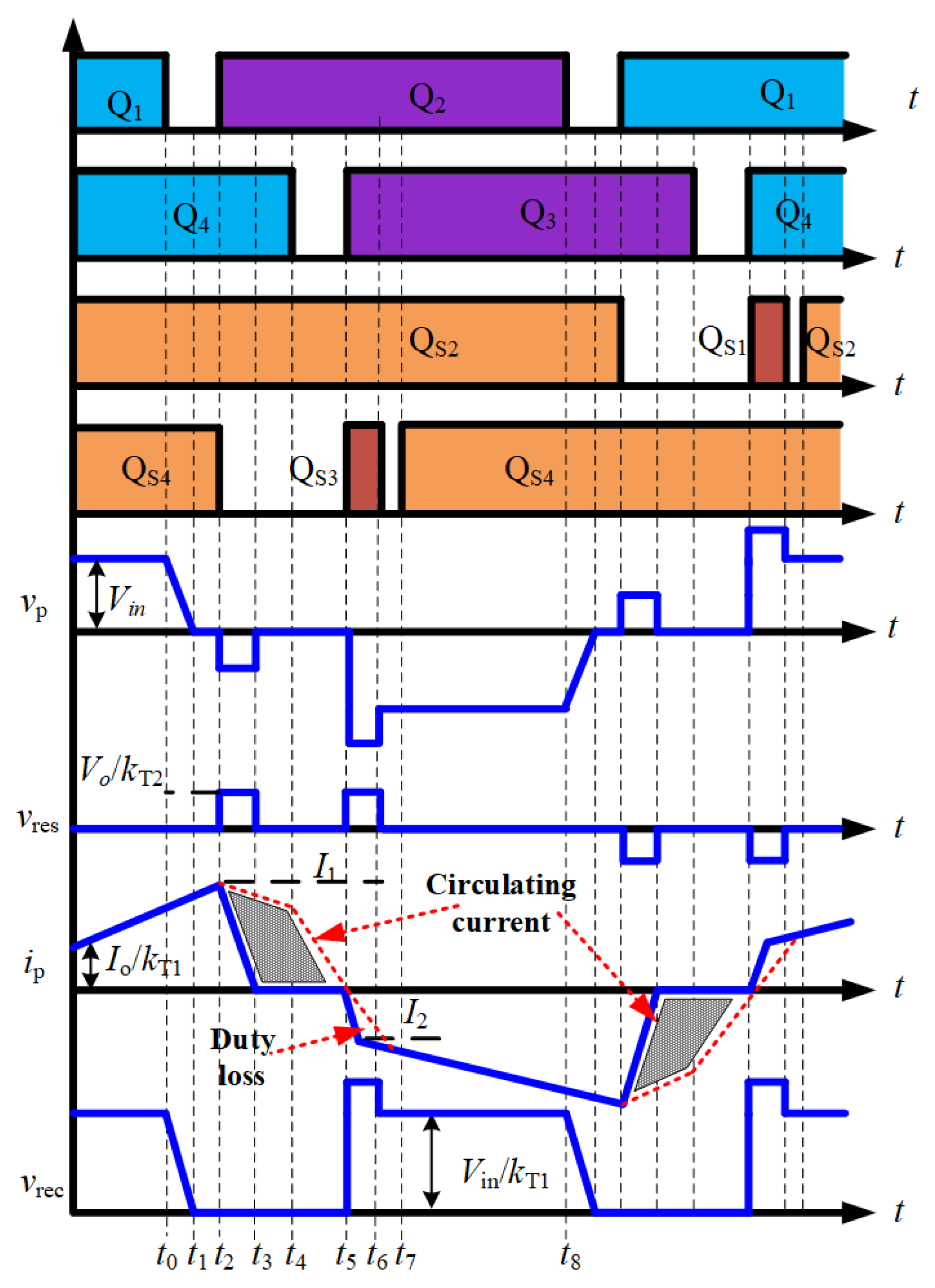
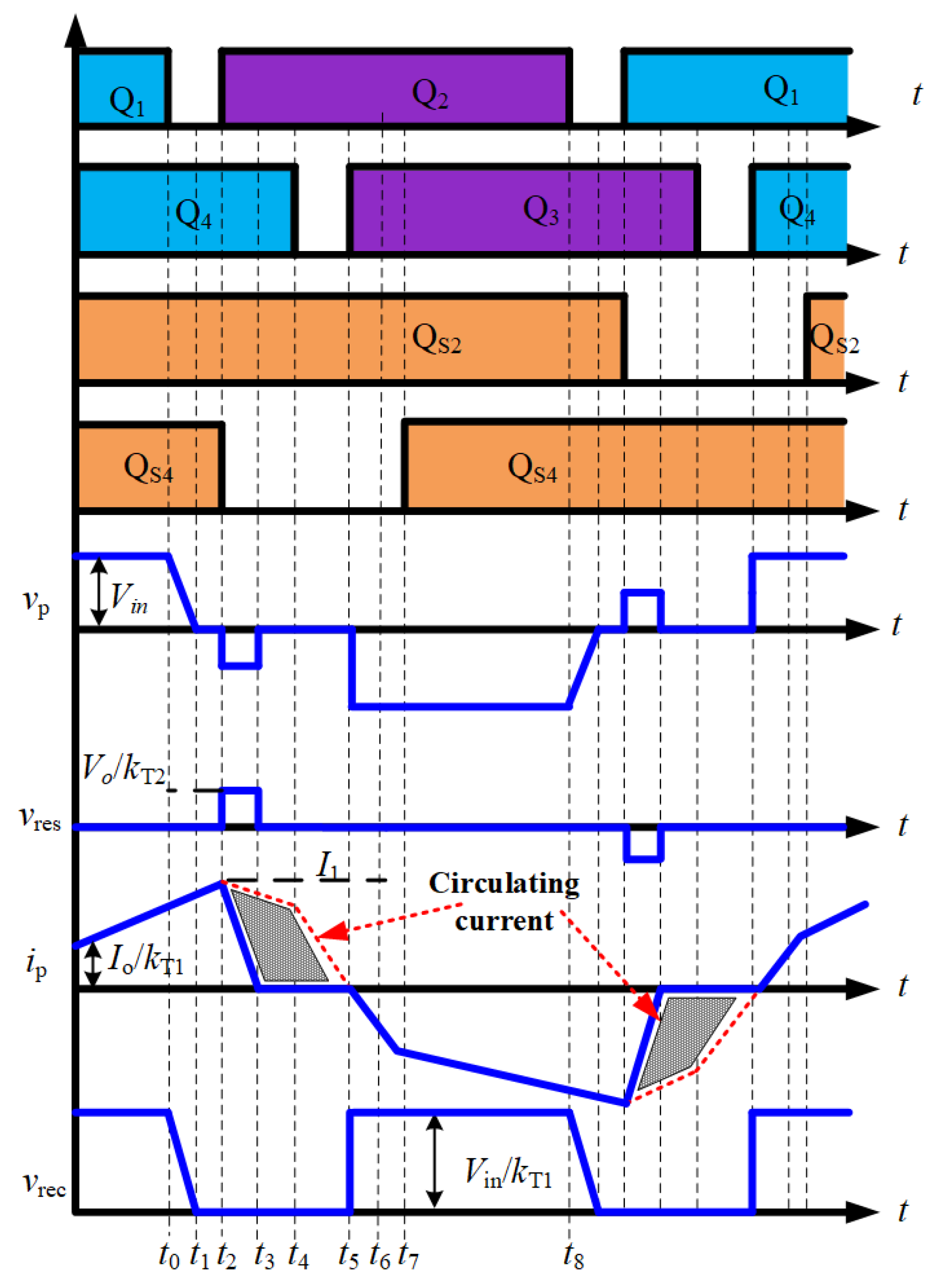
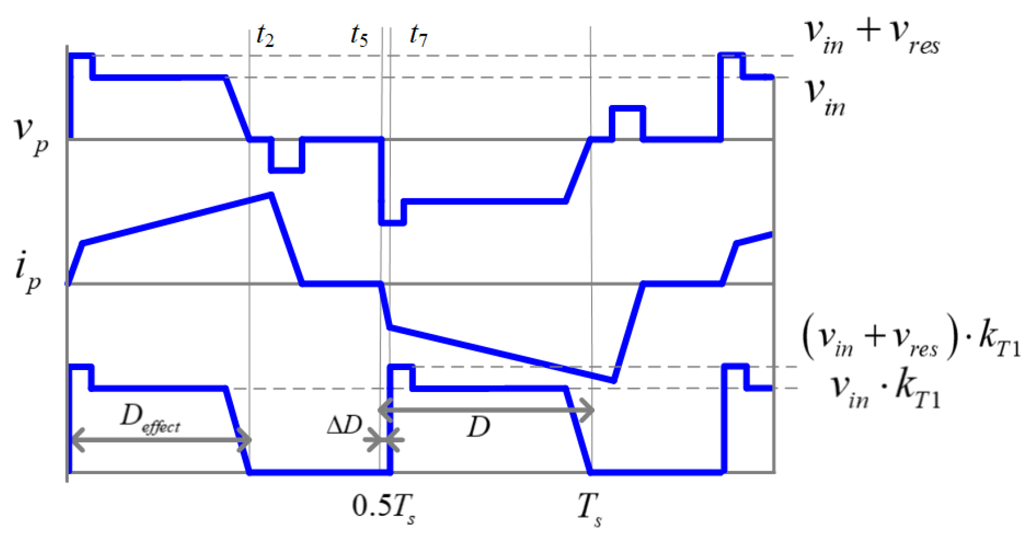
This converter can operate in two different modes according to the switching pattern of QS1 to QS4. These modes are named the normal mode and duty cycle enhanced mode. Figure 2 shows the core waveform of the steady state in the duty cycle enhanced mode, and the waveform of the normal mode is depicted in Figure 3. Figure 4 shows the equivalent circuits during the first half-switching cycle in each mode. Figure 4a–g represent the stages in the normal mode over one half-switching period, and Figure 4a–i give the stages in the duty cycle enhanced mode. In each mode, the operation procedure can be divided into two half periods over one switching cycle, and only one half period is analyzed for simplicity.
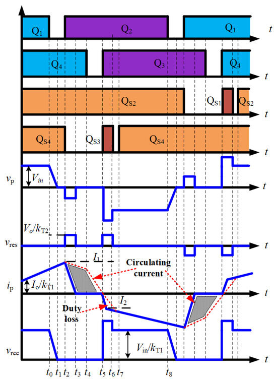
Figure 2.
Main operating waveform of the proposed circuit in duty cycle enhanced mode.
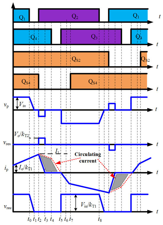
Figure 3.
Main operating waveform of the proposed circuit in normal mode.
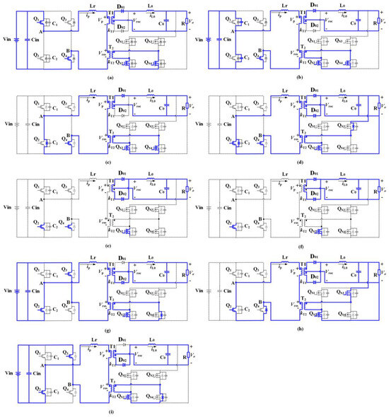
Figure 4.
Operating circuits in the first half-switching period: (a) Stage 1; (b) Stage 2; (c) Stage 3; (d) Stage 4; (e) Stage 5; (f) Stage 6; (g) Stage 7; (h) Stage 8 of duty enhanced mode; (i) Stage 9 of duty enhanced mode.
2.2. Normal Mode
When the circuit works in the normal mode, the primary current can decrease to zero quickly with the help of vres, and the ZCS of the lagging-leg switches can be guaranteed.
Stage 1 (Figure 4a, before t0): Before t0, Q1, and Q4 are on, T1 transfers power from the primary side to the secondary side and the load. QS2 and QS4 are also on, the secondary side of T2 free-wheels the primary current, and vres is zero.
In this mode, the circuit works in the normal power transformation period, and ip is decided by io. This stage ends when Q1 turns off.
Stage 2: (Figure 4b, t0–t1): At t0, Q1 turns off with ZVS due to C1. Then, C1 charges and C2 discharges during this stage. At the end of this stage, the voltage of C2 returns to zero and the voltage of C1 becomes Vin. The charge and discharge of C1 and C2 are due to the high value of Lo. This mode finishes when the voltage of Q2 is zero. In this mode, vp decreases with the following rate:
Stage 3 (Figure 4c, t1–t2): In this stage, the voltage of Q2 is zero and the circuit is still on with the help of the body diode. ip flows through D2 and Q4, and the primary circuit turns into the free-wheeling mode. ip and iT2 stay unchanged.
Stage 4 (Figure 4d, t2–t3): ip is resetting in this stage, and Q4, DS3, and Q2 are on. At t2, Q2 is on with ZVS, and QS4 is off simultaneously. Because of CS4, the voltage of QS4 cannot change sharply, and the switching-off loss is low. A partial current of QS4 turns to DS3.
During this stage, vres is applied to Llk, and ip decreases linearly. When ip is lower than IokT1, ILo goes through DO1 and DO2, and the secondary side is shorted.
In this circuit, the primary current ip can reset fast, entering the free-wheeling periods, and as shown in Figure 2, the circulating current can also decrease and is much lower than that of the conventional PSFB converter. In addition, Q3 and Q4 obtain a wide load range of ZVZCS.
Stage 5 (Figure 4e, t3–t4): At t3, when ip is zero, the current of the auxiliary circuit also decreases to zero. The body diode of QS3 turns off and the reset voltage vres becomes zero.
Stage 6 (Figure 4f, t4–t5): During the last stage, the current of the primary side is zero. Q4 turns off with ZCS at t4.
Stage 7 (Figure 4g, t5–t7): Because Llk limits the varying rating of ip, Q3 realizes a quasi-ZCS turning on at t7.
2.3. Duty Cycle Enhanced Mode
Stages 1–7 in this mode are the same as in the normal mode.
Stage 8 (Figure 4h, t5–t6): QS3 turns on at t7 and the current of the primary side ip flows through Q2 and Q4 and starts to increase in the opposite direction. The reset voltage overlays with vp, thus accelerating the reverse growth of ip, and the transformation of power can restart quickly. Because of the reduction in time of the freewheeling of the secondary side, the duty cycle loss can be largely reduced.
Stage 9 (Figure 4i, t6–t7): Q3 is on at t6, and QS3 is off. The primary side transfers power to the load, and Do1 is off because of the reverse voltage. Current in the auxiliary circuit flows through QS3 and DS4, and vres is zero. After t7, the circuit works in the next half stage.
In this mode, the reset voltage working as an excitation source creates a rapid growth of current to reduce the duty loss. In Figure 2, the dotted line is the waveform of the conventional PSFB, which grows much slower than the duty-enhanced working mode.
3. Performance Analysis and Comparison
3.1. Duty Cycle Loss
Duty cycle loss is the major problem of the conventional PSFB converter. It happens when ip cannot change immediately owing to Llk. Details of the duty cycle compensation in the proposed converter are given in Figure 5. The duty cycle loss is

Figure 5.
Calculation of duty cycle loss.
The actual duty cycle is
In Equation (8), D is the expected value of the duty cycle and Deff is the actual value.
The output voltage is
3.2. Condition of Soft-Switching
3.2.1. ZVZCS of Q1 to Q4
The leading-leg switches obtain ZVS easily with a high value of equivalent inductance. Hence, Q1 and Q2 ensure ZVS turning on over a wide load range. The condition of ZVS is
The minimum load current to ensure ZVS is
When Q1 and Q2 are turned off, C1 and C2 will restrain the rising speed of the voltage. Therefore, these switches operate with quasi ZVS turn-off.
Q3 and Q4 can achieve ZCS because ip decreases to zero before they are off. The rising speed of ip is restrained by Llk and vres. The condition of ZCS is
vres appears only in the free-wheeling modes, and it does not place much electrical stress on the main components [17,18].
When Q3 and Q4 are on, these switches can realize quasi-ZCS since ip cannot change immediately.
3.2.2. ZVZCS of Auxiliary Switches
The operation principles of QS1 and QS3 are the same, and the situations of QS2 and QS4 are identical.
In the normal mode, QS1 and QS3 are off permanently. QS2 and QS4 turn off with quasi-ZVS and turn on with ZCS. Hence, the switching loss is very low. In the duty cycle enhanced mode, QS2 and QS4 turn off and on with quasi-ZVS. QS1 and QS3 are on with quasi-ZCS and off with quasi-ZVS. Therefore, the power of QS1 to QS4 is a little higher than that of the normal mode.
3.3. Comparison
3.3.1. Consideration
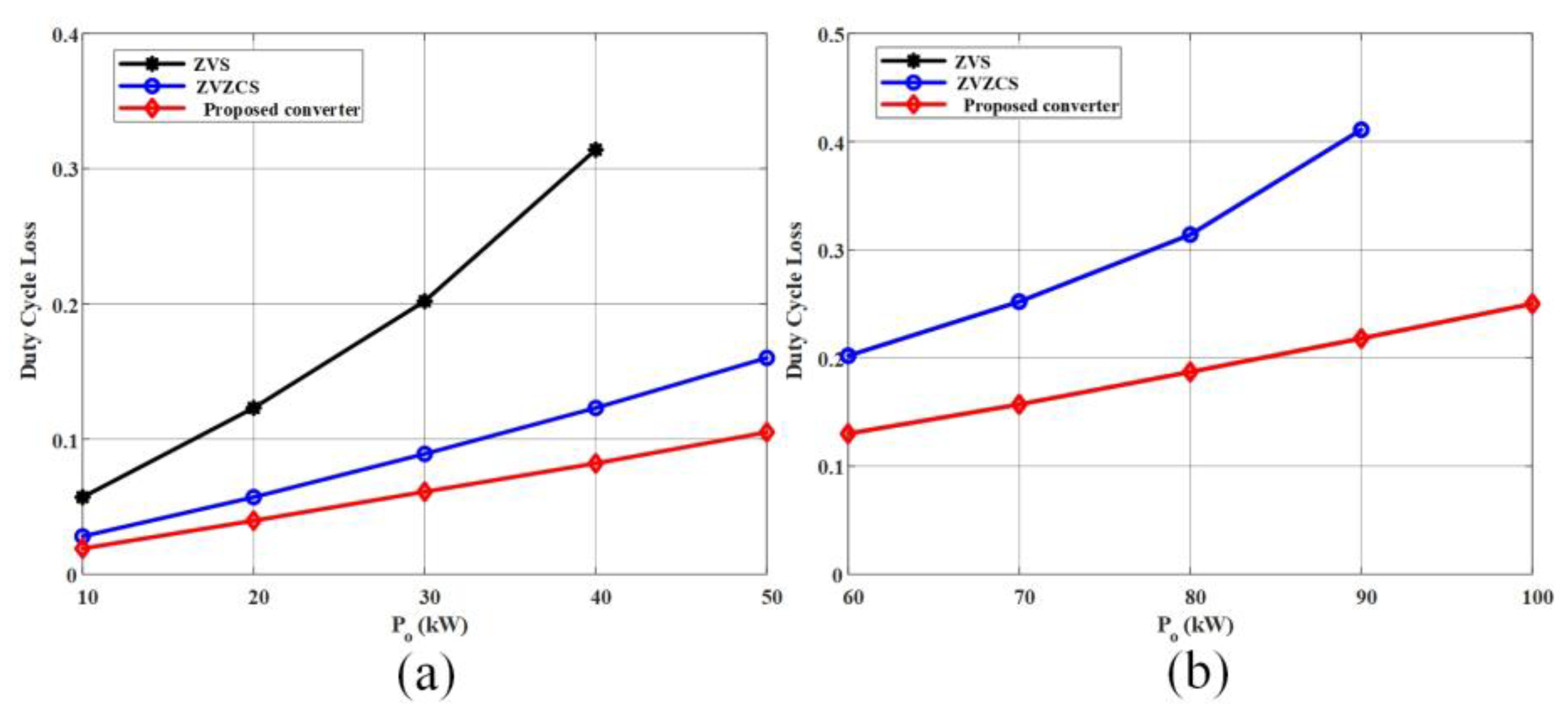
This paper uses the classical topology of the ZVZCS PSFB converter and ZVS PSFB converter, shown in Figure 6, to evaluate the proposed converter. The ZVZCS PSFB and the ZVS PSFB chosen here are common PSFBs (refer to [22,29,30]).
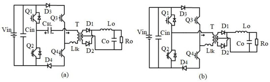
Figure 6.
Conventional converter for comparison: (a) conventional ZVS converter; (b) conventional ZVZCS converter.
The comparison is made with these baselines: the input voltage is 500 V (±20%), Vo is 28 V, and Po is 10 or 100 kW. The value of Llk is 10 µH, and the duty cycle is 1.
3.3.2. Performance Comparison
For the circuit in Figure 6a, the voltage press of the rectifier diodes will be influenced by the reset voltage of the primary current. During the reset course, the reset voltage will be added to the voltage press of the diodes. However, in the proposed circuit, the reset voltage will only appear in the free-wheeling stage and will not influence the rectifier diodes. For the circuit in Figure 6b, the components of the primary side will suffer from an inrush current in operation. Both the reset voltage and the inrush current will increase the power loss of the circuit, and the dash current will apparently limit the power range of the operation condition. As a result, for these two compared circuits, the soft-switching ranges are narrower than for the proposed circuit because of the loss of duty cycle and the limitation of the power rating. The detailed calculation of the loss of duty cycle below shows that the smallest loss is for the proposed circuit.
As shown in Table 1, the number of components in the proposed circuit is larger than those for the circuits in Figure 6a,b, which is the main drawback of this converter. However, the proposed converter can reset the primary current under any power rating with a specific design of T2, which may be the only choice in high-power applications. Therefore, it is challenging to apply the proposed converter in high-power industrial applications.

Table 1.
Performance comparison.
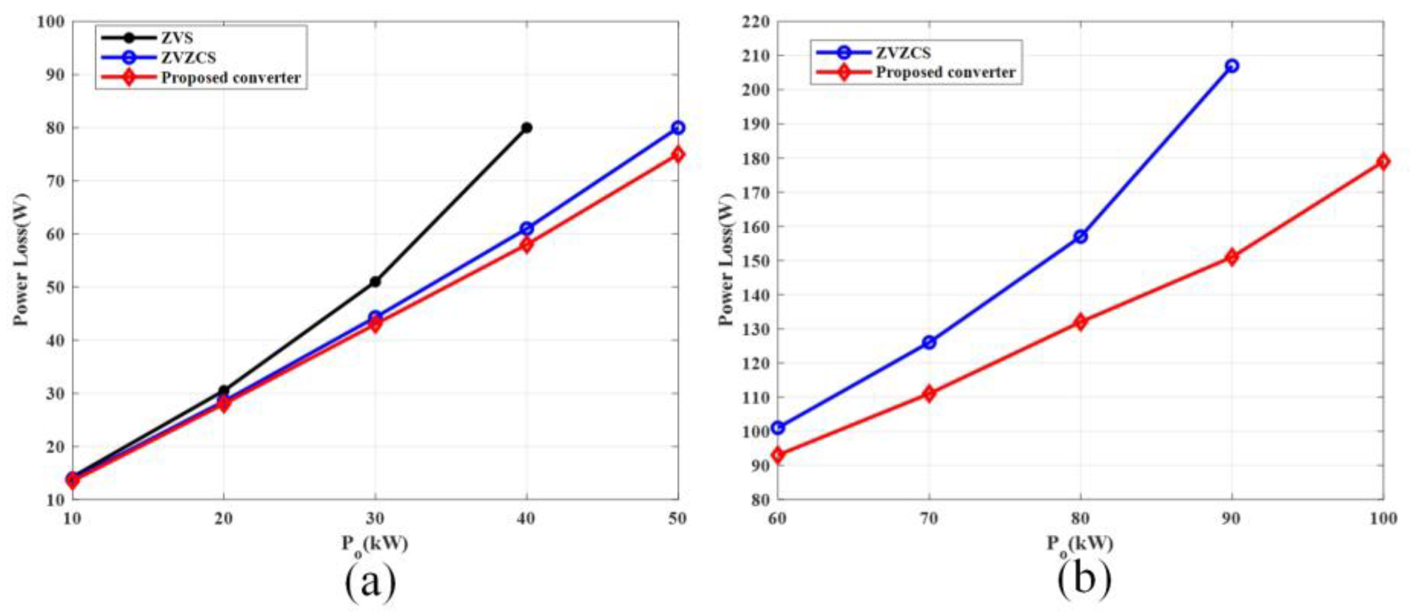
As can be seen in Table 1 and Figure 7, the proposed converter has the minimum duty cycle loss. For comparison, the duty cycle losses and turns ratios of other converters were calculated using Equations (13) and (14). When Po reaches 50 kW, the duty cycle loss of the ZVS circuit is over 0.5 and the primary side will not have power transmission to the secondary side. When Po is higher than 40 kW, the ZVS converter cannot work normally and the duty cycle loss is beyond the reasonable range. When Po is higher than 90 kW, the conventional ZVZCS converters have the same situation.
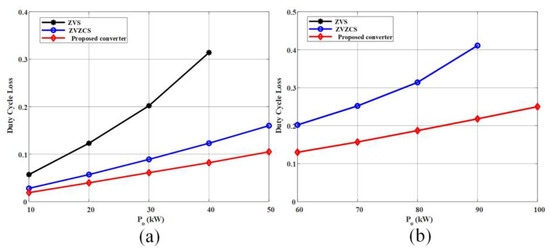
Figure 7.
Comparison of duty cycle loss: (a) duty cycle loss of ZVS, ZVZCS, and proposed converter (Po = 10 kW–50 kW); (b) duty cycle loss of ZVZCS and proposed converter (Po = 60 kW–100 kW).
The transformer voltage ratio is the key parameter. When the turns ratio is high, in the same condition, the current of the primary side is low and so is the voltage press of the rectifier diodes. Thus, the conduction loss and cost will be low. But a high turns ratio will cause a low output voltage because of the duty cycle loss.
For the converter in Figure 6, Llk causes serious duty cycle loss under high-power and low-input-voltage conditions. Therefore, the turns ratio must be lowered to compensate for the duty cycle loss. However, in the proposed converter, the duty cycle loss can be effectively reduced with the help of the reset voltage vres provided by the auxiliary transformer. Thus, the turns ratio of T1 in the proposed converter can be optimized, and the expected performance of the proposed converter is high.
When the DC bus voltage is 400 V, the duty cycle losses of the three circuits are
ΔDpro is the duty cycle loss of the proposed converter, ΔDZVZCS is the duty cycle loss of the converter in Figure 6a, and ΔDZVS is the duty loss in Figure 6b.
The secondary voltage can be calculated as
VD = 1.5 V and VLo = 0.5 V are the voltage drops on the rectifier inductor. Furthemore, the turns ratios under 10 kW are
where npro is the turns ratio of T1 in the proposed circuit, nZVZCS is the turns ratio of the conventional ZVZCS PSFB converter in Figure 6a, and nZVS is the turns ratio of the conventional ZVS PSFB converter in Figure 6b.
Under 90 kW, the turns ratios are
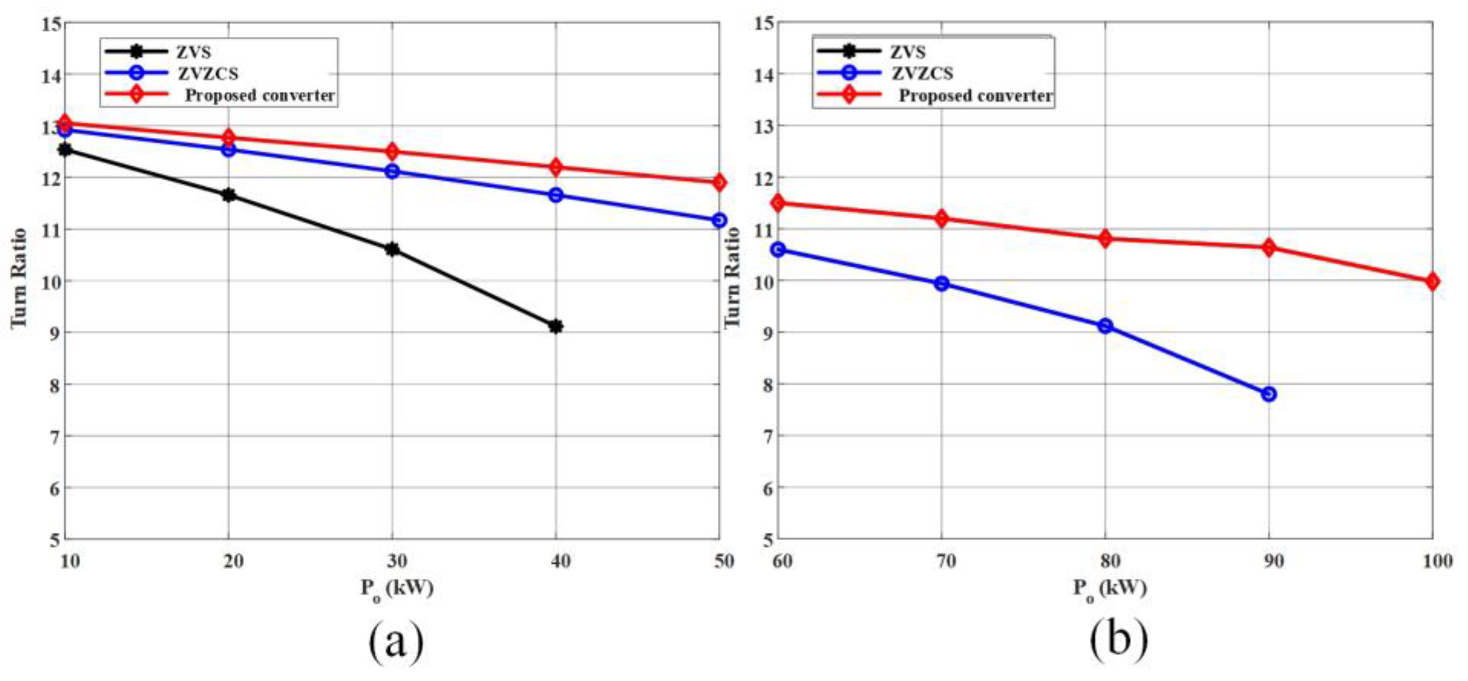
As shown in Figure 7, when Po is under 50 kW, it is obvious that the ZVS converter loses more duty cycle than the conventional ZVZCS converter and the proposed converter. When Po is higher than 50 kW, the proposed converter has more advantages in duty cycle loss. As shown in Figure 8, this has a great influence on the optimization of the transformer. Compared with the conventional ZVZCS PSFB converter, the optimization of the turns ratio can reach 40%. Moreover, the decrease in the power loss of the primary side can be seen in Figure 9.
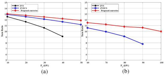
Figure 8.
Variable turns ratio: (a) ZVS, ZVZCS, and the proposed converter (Po = 10 kW–50 kW); (b) ZVZCS and the proposed converter (Po = 60 kW–100 kW).
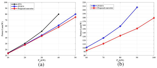
Figure 9.
Comparison of conduction loss: (a) ZVS, ZVZCS, and the proposed converter (Po = 10 kW–50 kW); (b) ZVZCS and the proposed converter (Po = 60 kW–100 kW).
To realize a rapid reset of the primary current, this circuit uses a variable voltage provided by the auxiliary circuit. The rapid and effective recovery of ip can break the power range limitation of the existing ZVZCS converters. Therefore, the proposed converter is well-suited to high-power applications.
4. Experiments’ Results
To verify the proposed converter, a laboratory prototype was built. The key parameters of the circuit are shown in Table 2. The switching frequency is 20 kHz considering IGBT with a high current rating.
Table 2.
Main parameters of the experiment.
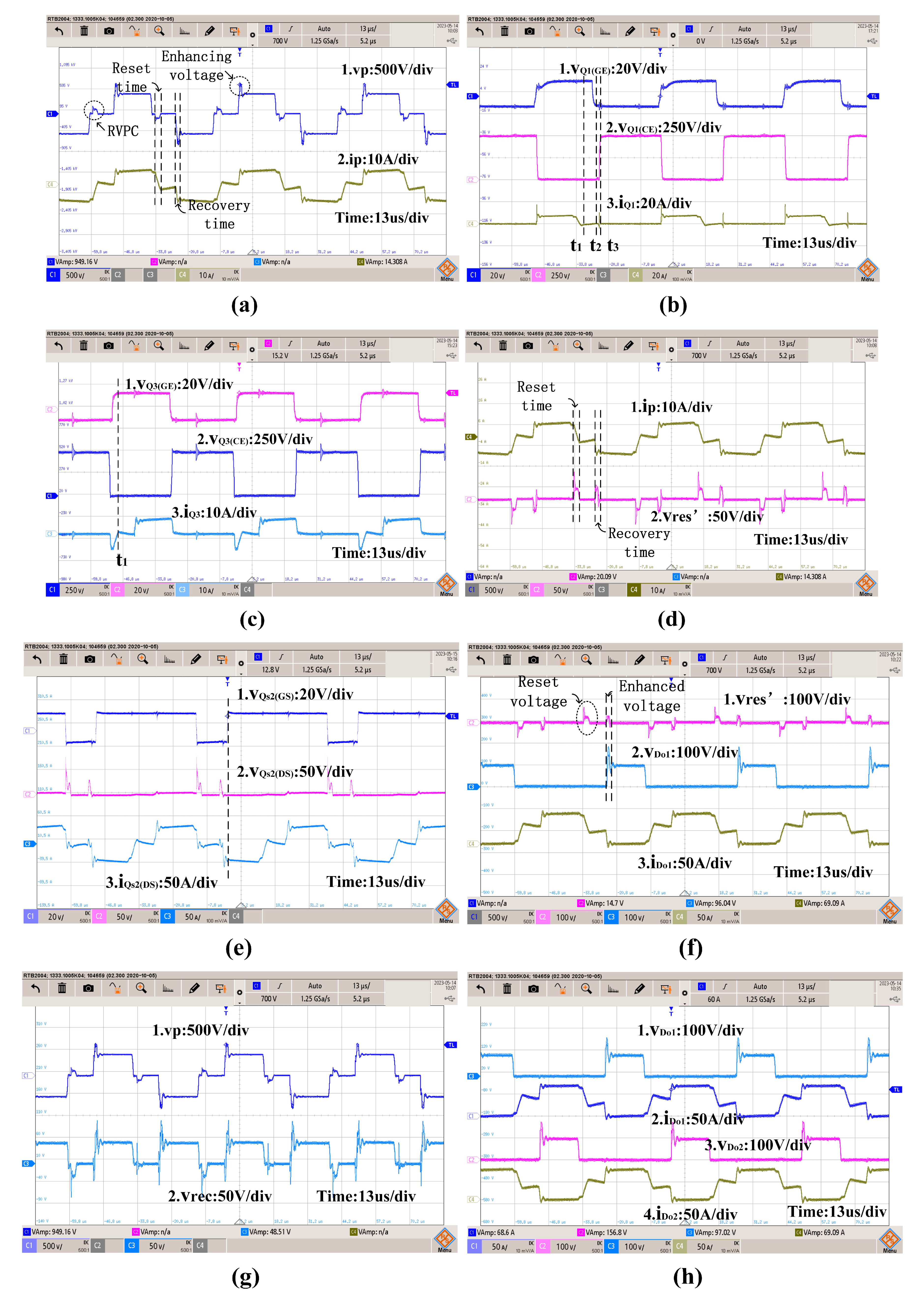
Figure 10 shows the experiments’ results for the proposed converter.
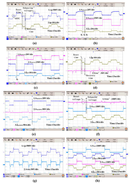
Figure 10.
Experiments’ results: (a) vp and ip; (b) vQ1(GE), vQ1(CE), and iQ1; (c) vQ3(GE), vQ3(CE), and iQ3; (d) ip and vres’; (e) vres, vDo1 and iDo1, and iQs2; (f) vDo1, iDo1, vDo2, and iDo2; (g) vp and vDo1; (h) vp and vDo1 in normal mode.
For the convenience of presentation, the common characteristics are illustrated with the results from the duty cycle enhanced mode, and the special waveform of the normal mode is provided in Figure 10h. As shown in Figure 10a, vres is 168 V after t1, and ip decreases. The circle with dashed lines is the reset time in Figure 10a. With the turns ratio of T2 changing, the circuit can have different reset voltages and can operate in good conditions when the load changes even in high-power applications, which means no existing power rating limitation. In Figure 10a, vp has a spike at the beginning of the power transfer stages, which can minimize the duty cycle loss. As the duty cycle enhanced mode is only used in the low-input-voltage mode, this spike does not increase the voltage rating of the rectifier diode. As shown in Figure 10h, there is no voltage spike in the normal mode.
The ZVS operation of Q1 and Q2 is depicted in Figure 10b, and they can realize ZVS over a wide load range with the help of the output inductor. In this picture, D1 conducts and vQ1(CE) reduces to zero before t1; then, vQ1(GE) reaches the threshold voltage at t2. Hence, Q1 and Q2 in the proposed circuit turn on with ZVS.
Figure 10c shows that Q3 and Q4 can realize ZCS over a wide load range because ip is decreased to zero at corresponding switching-off instants. At t1, when vQ3(GE) is about 15 V, iQ3 reaches zero. At t1, vQ3(GE) is about −10 V, meaning that Q3 is already off with ZCS. In Figure 10c, vQ3 has a current spike at t3. Figure 4f,g give the equivalent circuits, and the mechanism of the spike is described as follows. In Figure 10f, vQ3 = vB = vA = 0, and vQ3 remains at zero in this stage. After Q4 is on, the input voltage charges C3, which causes a current spike. The energy of the spike will be stored in Co and will be released at the next instant of switching on. Thus, the power loss is low.
The voltage and current of transformer T2 can be seen in Figure 10d. vres only appears in the current reset mode and the duty cycle enhanced mode. The current of the secondary side is ip and that of the primary side of T2 is ip/kT2. The integration of T1 and T2 may reduce the volume and may be investigated in future work.
In Figure 10e, the increase in the voltage stress of the rectifier diodes will only happen when duty cycle enhanced mode is applied because the voltage of the DC bus is low, and the enhancing voltage is also adjustable so there is no extra voltage stress added to the diodes, which agrees well with the theoretical analysis. This can be seen in the comparison of Figure 10g,h. Since the efficiency is influenced by the VA rating of the rectifier diodes, the proposed converter will have a better performance in high-power applications.
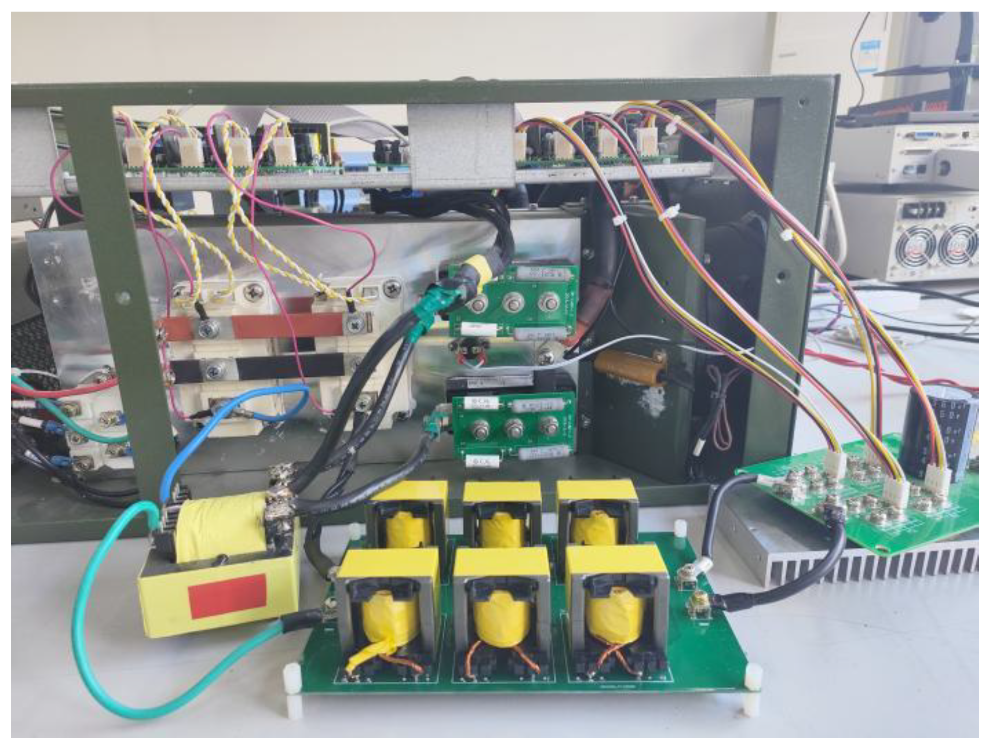
As shown in Figure 11, the efficiency grows with the load. According to the component parameters, we expected the maximum efficiency of the proposed converter to be about 96%. In Figure 11b, the power loss is about 100 W and the maximum efficiency is around 96%. The rectifier diodes on the secondary side generate about 70 W power loss, which represents the majority of the overall power loss. To further increase efficiency, a synchronous rectifier can be adopted. Figure 12 shows a photo of the prototype. To limit the leakage inductance and have a higher efficiency, T2 uses six small transformers and each of them is 1:1.
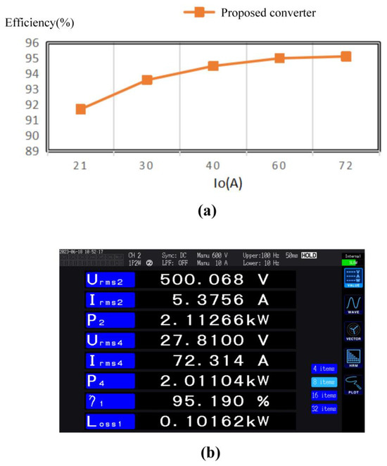
Figure 11.
Efficiency: (a) η with Io; (b) hard copy of efficiency.

Figure 12.
Photo of the proposed prototype.
5. Conclusions
In this article, we have proposed a ZVZCS PSFB converter, which can reset the primary current and reduce duty cycle loss. For applications in EV batteries, the proposed circuit will minimize duty cycle loss while avoiding significantly increasing the overall power loss of the circuit. Thus, the efficiency of power transmission can be greatly increased and the charging time can be shortened. Furthermore, the realization of ZVZCS can reduce the amount of heat because of power loss and can help prolong the battery life. Specifically, this circuit has the following advantages:
- (1)
- The duty cycle loss can be reduced effectively, and the circuit can be optimized;
- (2)
- The primary switches can realize soft-switching over a wide load range and the additional power loss caused by the auxiliary circuit is low;
- (3)
- The ZVZCS operation has no power rating limitation;
- (4)
- The electrical stress of the components is much lower than that of the conventional ZVZCS PSFB converter.
Further work may include efforts toward the optimization of the auxiliary transformer, lower loss on rectifier diodes, and circuit integration.
Author Contributions
Methodology, Y.S.; Resources, Y.S.; Writing—original draft, Y.W.; Writing—review & editing, Y.W., Y.S. and K.X.; Supervision, Y.S. and K.X. All authors have read and agreed to the published version of the manuscript.
Funding
This research was funded by the Key Research and Development Projects of Shaanxi Province (grant number 2024GX-YBXM-281).
Data Availability Statement
The data presented in this study are available in this article.
Conflicts of Interest
The authors declare no conflict of interest.
References
- Dusmez, S.; Hasanzadeh, A.; Khaligh, A. Loss analysis of non-isolated bidirectional DC/DC converters for hybrid energy storage system in EVs. In Proceedings of the 2014 IEEE 23rd International Symposium on Industrial Electronics (ISIE), Istanbul, Turkey, 1–4 June 2014; pp. 543–549. [Google Scholar]
- Dusmez, S.; Khaligh, A. A Supervisory Power-Splitting Approach for a New Ultracapacitor–Battery Vehicle Deploying Two Propulsion Machines. IEEE Trans. Ind. Inform. 2014, 10, 1960–1971. [Google Scholar] [CrossRef]
- Khaligh, A. Realization of Parasitics in Stability of DC–DC Converters Loaded by Constant Power Loads in Advanced Multiconverter Automotive Systems. IEEE Trans. Ind. Electron. 2008, 55, 2295–2305. [Google Scholar] [CrossRef]
- Lee, D.-W.; Youn, H.-S.; Kim, J.-K. Development of Phase-Shift Full-Bridge Converter with Integrated Winding Planar Two-Transformer for LDC. IEEE Trans. Transp. Electrif. 2023, 9, 1215–1226. [Google Scholar] [CrossRef]
- Shen, J.; Hasanzadeh, A.; Khaligh, A. Optimal power split and sizing of hybrid energy storage system for electric vehicles. In Proceedings of the 2014 IEEE Transportation Electrification Conference and Expo (ITEC), Dearborn, MI, USA, 15–18 June 2014; pp. 1–6. [Google Scholar]
- Lyu, D.; Soeiro, T.B.; Bauer, P. Design and Implementation of a Reconfigurable Phase Shift Full-Bridge Converter for Wide Voltage Range EV Charging Application. IEEE Trans. Transp. Electrif. 2023, 9, 1200–1214. [Google Scholar] [CrossRef]
- Ochoa, D. Extension of the Injected-Absorbed-Current Method Applied to DC–DC Converters with Input Filter, Output Postfilter, and Feedforward Compensations. IEEE Trans. Transp. Electrif. 2022, 8, 856–874. [Google Scholar] [CrossRef]
- Zhao, L.; Li, H.; Wu, X.; Zhang, J. An Improved Phase-Shifted Full-Bridge Converter with Wide-Range ZVS and Reduced Filter Requirement. IEEE Trans. Ind. Electron. 2018, 65, 2167–2176. [Google Scholar] [CrossRef]
- Zhu, Y.; Guo, Z.; Geng, Q. An Improved Full-Bridge Converter with a Five-Diode Rectifier for High Efficiency in Wide Voltage Range. IEEE Trans. Power Electron. 2022, 37, 3178–3191. [Google Scholar] [CrossRef]
- Chen, W.; Ruan, X.; Zhang, R. A novel zero-voltage-switching PWM full bridge converter. IEEE Trans. Power Electron. 2008, 23, 793–801. [Google Scholar] [CrossRef]
- Chen, W.; Ruan, X.; Chen, Q.; Ge, J. Zero-voltage-switching PWM fullbridge converter employing auxiliary transformer to reset the clamping diode current. IEEE Trans. Power Electron. 2010, 25, 1149–1162. [Google Scholar] [CrossRef]
- Han, J.-K.; Moon, G.-W. High-Efficiency Phase-Shifted Full-Bridge Converter with a New Coupled Inductor Rectifier (CIR). IEEE Trans. Power Electron. 2019, 34, 8468–8480. [Google Scholar] [CrossRef]
- Jang, Y.; Jovanovic, M.M. A New PWM ZVS Full-Bridge Converter. IEEE Trans. Power Electron. 2007, 22, 987–994. [Google Scholar] [CrossRef]
- Chen, J.; Liu, C.; Liu, H.; Li, G. Zero-Voltage Switching Full-Bridge Converter With Reduced Filter Requirement and Wide ZVS Range for Variable Output Application. IEEE Trans. Ind. Electron. 2021, 69, 6805–6816. [Google Scholar] [CrossRef]
- Guo, Z.; Sha, D.; Liao, X.; Luo, J. Input-Series-Output-Parallel Phase-Shift Full-Bridge Derived DC–DC Converters with Auxiliary LC Networks to Achieve Wide Zero-Voltage Switching Range. IEEE Trans. Power Electron. 2014, 29, 5081–5086. [Google Scholar] [CrossRef]
- Yang, Y. An Improved Control Scheme for Reducing Circulating Current and Reverse Power of Bidirectional Phase-Shifted Full-Bridge Converter. IEEE Trans. Power Electron. 2022, 37, 11620–11635. [Google Scholar] [CrossRef]
- Dudrik, J.; Spanik, P.; Trip, N.D. Zero-Voltage and Zero-Current Switching Full-Bridge DC–DC Converter with Auxiliary Transformer. IEEE Trans. Power Electron. 2006, 21, 1328–1335. [Google Scholar] [CrossRef]
- Wu, X.; Xie, X.; Zhang, J.; Zhao, R.; Qian, Z. Soft switched full bridge DC-DC converter with reduced circulating loss and filter requirement. IEEE Trans. Power Electron. 2007, 22, 1949–1955. [Google Scholar] [CrossRef]
- Luo, J.; Guo, Z.; Zhan, W.; Chen, S. Efficient Hybrid Dual Full-Bridge DC–DC Converters for Pulsed Output Current Applications. IEEE Trans. Ind. Electron. 2023, 70, 12254–12266. [Google Scholar] [CrossRef]
- Lakshmi, P.V.; Musala, S.; Srinivasulu, A.; Ravariu, C. Design of a 0.4 V, 8.43 ENOB, 5.29 nW, 2 kS/s SAR ADC for Implantable Devices. Electronics 2023, 12, 4691. [Google Scholar] [CrossRef]
- Wu, X.; Xie, X.; Zhao, C.; Qian, Z.; Zhao, R. Low voltage and current stress ZVZCS full bridge DC-DC converter using center tapped rectifier reset. IEEE Trans. Ind. Electron. 2008, 55, 1470–1477. [Google Scholar] [CrossRef]
- Ruan, X.; Yan, Y. A novel zero-voltage and zero-current-switching PWM full-bridge converter using two diodes in series with the lagging leg. IEEE Trans. Ind. Electron. 2001, 48, 777–785. [Google Scholar] [CrossRef]
- Seok, K.; Kwon, B. An improved zero-voltage and zero-currentswitching full-bridge PWM converter using a simple resonant circuit. IEEE Trans. Ind. Electron. 2001, 48, 1205–1209. [Google Scholar] [CrossRef]
- Shi, Y.; Feng, L.; Li, Q.; Kang, J. High Power ZVZCS Phase Shift Full Bridge DC–DC Converter with High Current Reset Ability and No Extra Electrical Stress. IEEE Trans. Ind. Electron. 2022, 69, 12688–12697. [Google Scholar] [CrossRef]
- Yu, W.; Lai, J.-S.; Lai, W.-H.; Wan, H. Hybrid Resonant and PWM Converter with High Efficiency and Full Soft-Switching Range. IEEE Trans. Power Electron. 2012, 27, 4925–4933. [Google Scholar] [CrossRef]
- Lim, C.-Y.; Jeong, Y.; Moon, G.-W. Phase-Shifted Full-Bridge DC–DC Converter with High Efficiency and High Power Density Using Center-Tapped Clamp Circuit for Battery Charging in Electric Vehicles. IEEE Trans. Power Electron. 2019, 34, 10945–10959. [Google Scholar] [CrossRef]
- Gao, Y.; Tang, Y.; Sun, H.; Guo, Y.; Liu, G.; Yang, H. Variable Saturation Inductor-Based Full Bridge Converter with Wide ZVS Range and Reduced Duty Cycle Loss. IEEE Trans. Ind. Electron. 2022, 69, 11055–11066. [Google Scholar] [CrossRef]
- Gao, Y.; Tang, Y.; Yao, F.; Ge, L.; Guo, Y.; Sun, H. Paralleled Variable Inductor Phase-Shifted Full-Bridge Converter with Full Load Range ZVS and Low Duty Cycle Loss. IEEE Trans. Ind. Electron. 2023, 71, 154–196. [Google Scholar] [CrossRef]
- Hua, G.; Lee, F.C.; Jovanovic, M.M. An improved full-bridge zero-voltage-switched PWM converter using a saturable inductor. IEEE Trans. Power Electron. 1993, 8, 530–534. [Google Scholar] [CrossRef]
- Jang, Y.; Jovanovic, M.M. A new family of full-bridge ZVS converters. IEEE Trans. Power Electron. 2004, 19, 701–708. [Google Scholar] [CrossRef]


Disclaimer/Publisher’s Note: The statements, opinions and data contained in all publications are solely those of the individual author(s) and contributor(s) and not of MDPI and/or the editor(s). MDPI and/or the editor(s) disclaim responsibility for any injury to people or property resulting from any ideas, methods, instructions or products referred to in the content. |
© 2024 by the authors. Licensee MDPI, Basel, Switzerland. This article is an open access article distributed under the terms and conditions of the Creative Commons Attribution (CC BY) license (https://creativecommons.org/licenses/by/4.0/).