Article

An Enhanced Verilog-A Model for Graphene Field-Effect Transistors Using Variable Fermi Velocity

1
Department of Electrical, Computer, and Systems Engineering, Case Western Reserve University, Cleveland, OH 44106, USA
2
NASA Glenn Research Center, Cleveland, OH 44135, USA
*
Author to whom correspondence should be addressed.
Electronics 2024, 13(24), 5051; https://doi.org/10.3390/electronics13245051
Submission received: 29 October 2024 / Revised: 18 December 2024 / Accepted: 19 December 2024 / Published: 23 December 2024

Abstract

:
This paper presents a novel Verilog-A model for the Fermi velocity in Graphene Field-Effect Transistors (GFETs). The Fermi velocity is an important parameter associated with the energy spectrum of the delocalized bonds in graphene which impact the performance of a GFET. Unlike existing GFET models where the Fermi velocity is assumed to have a constant value, the proposed model considers carrier concentrations in the channel and gate dielectrics to create a closed-form solution for the Fermi velocity, a parameter previously demonstrated to vary based on these two factors. The proposed mathematical model is then adapted to Verilog-A for interfacing with computer-aided design (CAD) circuit simulators. To demonstrate the accuracy of the proposed model, the simulation results are compared to measured drain–source currents obtained from various GFET devices (including GFETs measured by authors). The measured results show good agreement with the values predicted using the proposed model (<±1%), demonstrating the superior accuracy of the model compared to other published Verilog-A-based models, especially around the Dirac point.

1. Introduction

Graphene is a material of interest for high-frequency applications due to its high carrier mobility. Graphene Field-Effect Transistors (GFETs) have garnered interest for use in high-frequency circuits due to their ambipolar conduction (i.e., conduction via holes or electrons) [1]. However, the lack of a universally applicable model that can accurately predict device performance has impacted the adoption of this technology in analog integrated circuits. Creating an accurate GFET model has proven to be very challenging due to the lack of closed-form solutions for the ambipolar charge, quantum capacitance, Fermi velocity, and carrier mobility [2,3].
Mathematical models for a GFET have been through many iterations while under development, with many different authors contributing towards creating a complete model. By incorporating the work by Fang et al. [4] on charge carrier concentrations in graphene, Thiele et al. developed the first dual-gated GFET model that incorporates the dependence of charge carrier behavior on the channel voltage, quantum capacitance, and saturation velocity [2,5]. Wang et al. built upon this work to create a compact virtual-source GFET model that considers source resistance, mobility saturation, and simplified 1D electrostatics [6]. Separately, Parrish et al. introduced an accurate quantum capacitance approximation and the concept of symmetric channel charge [7]. Shortly thereafter, the first Verilog-A-based GFET model was created by Rodriguez et al. [8] and enhanced by Landauer et al. by introducing adjustments to previous mathematical models, making them more compatible with closed-form solutions [9]. Furthermore, a novel channel voltage solution method, compatible with Verilog-A, was introduced [9]. Finally, Tian et al. introduced a new mobility model, considering both hole and electron contributions, and created new, simplified mathematical models of the saturation velocity and capacitance weighting factor [3,10]. Despite these numerous improvements, the aforementioned models do not properly represent the Fermi velocity, resulting in inaccuracies in calculating channel conduction. This paper describes an effort to address this issue by improving Tian et al.’s effective mobility model and creating a novel Fermi velocity solution method. This Fermi velocity solution method takes advantage of the computational power of the CAD tools, such as the Keysight’s Advanced Design System (ADS), to concurrently solve for the Fermi velocity at every iteration of the simulation. The remainder of this paper is organized as follows: Section 2 provides an overview of the existing GFET models and their deficiencies. Section 3 describes the development of the novel Fermi velocity model, followed by the implementation and validation steps in Section 4 and the conclusions in Section 5.

2. Evolution of GFET Models

2.1. Fermi Velocity

A critically important parameter in accurate GFET modeling is the Fermi velocity, as it significantly influences the drain current of a GFET. The Fermi velocity is used to describe the energy spectrum of the delocalized π bonds in graphene, which results from its SP2 hybridization. Using a tight-binding Hamiltonian analysis, the energy spectrum of the first Brillouin zone for graphene may be calculated using E ( k ) = s v f | k | , where v f is the Fermi velocity, is the reduced Planck’s constant, s is ±1 (+1 for the conduction band and −1 for the valence band), and k is the momentum [4]. Conversely, the Fermi velocity exhibits an inverse relationship to several key GFET parameters, such as the mobility, charge density, and quantum capacitance. A lower Fermi velocity value is preferred, with the ideal value calculated to be 0.85 × 10⁶ m/s, as derived from suspended metallic carbon nanotubes [11]. Traditionally, GFET models utilize a constant Fermi velocity of 1 × 10⁶ m/s. However, the Fermi velocity has been demonstrated to be significantly influenced by the choice of gate dielectric material and doping [11,12]. Therefore, accurate GFET modeling must incorporate substrate effects on the Fermi velocity.

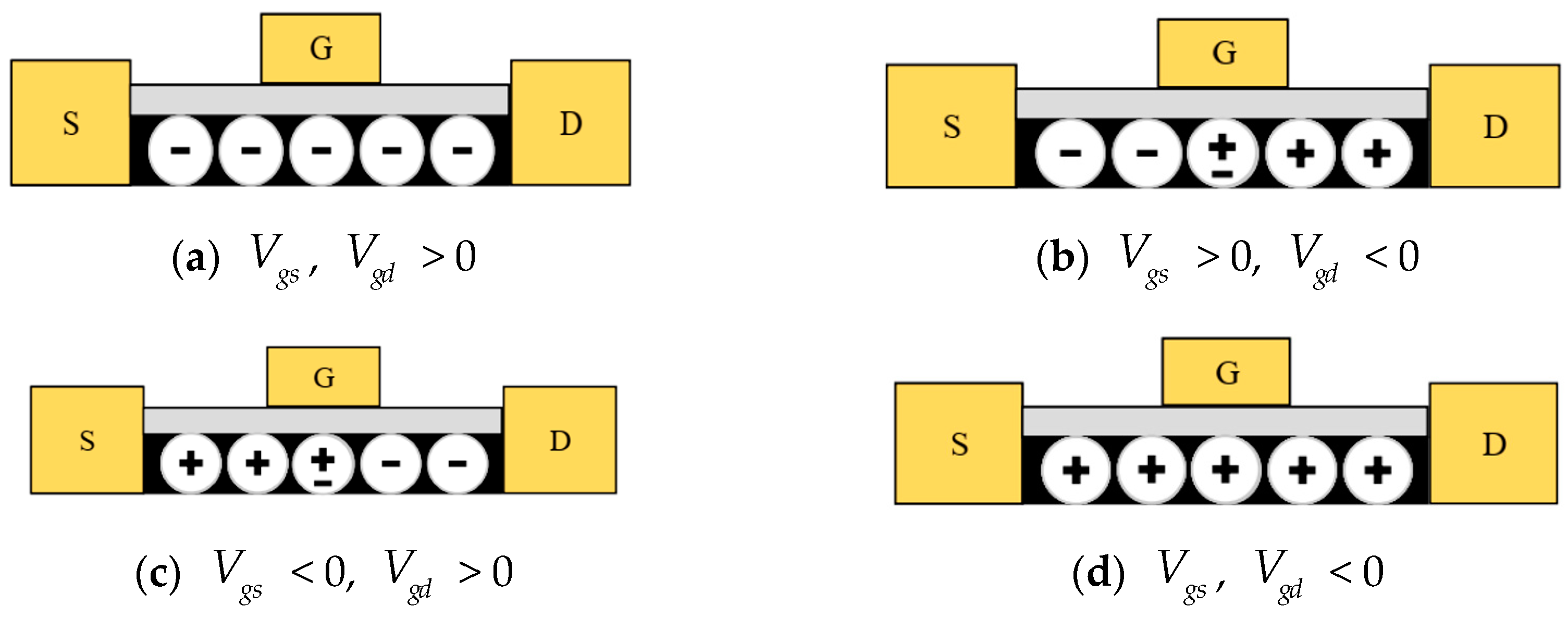
2.2. Revisiting the Dual-Gated GFET Model

One of the most important derivations to result from Thiele et al.’s dual-gated GFET model [5] is the general drain current equation, derived from the drift–diffusion equation and the drift velocity of graphene:
I D = W 0 V D S μ q ρ s h d V L + | 0 V D S μ 1 v s a t d V | ,
where µ is the mobility, q is the elementary charge, ρ s h is the charge sheet density, v s a t is the saturation velocity, W and L are the width and length of the gates, and VDS denotes the drain–source voltage of the GFET, respectively. The term q ρ s h is the total charge within the channel, which is expressed as [9]
Q t o t = q ρ s h = Q t + q n p u d ,
where Qt is the total charge in the channel and n p u d is the number of puddles, a value that adjusts for the trapped charges. The total channel charge, Qt, may be calculated by finding the channel’s sum of the hole and electron charges, which have each been previously modeled mathematically by Thiele et al. [2,5]:
p = 2 ( k B T ) 2 π ( v F ) 2 F 1 ( q V c h k B T ) ,
n = 2 ( k B T ) 2 π ( v F ) 2 F 1 ( q V c h k B T ) ,
where k B is Boltzmann’s constant, T is the temperature, is the reduced Planck’s constant, v F is the Fermi velocity, q is the elementary charge of an electron, and V c h is the voltage in the transistor’s channel, respectively. F1(x) is the first-order Fermi–Dirac approximation in accordance with [13,14]. The total channel charge, Qt, may now be calculated by summing the electron and hole densities and multiplying the result by the charge [2,9]:
Q t = q π ( k B T ) 2 3 ( v F ) 2 + q 3 V c h 2 π ( v F ) 2
By assuming an even distribution of holes and electrons, n p u d may be modeled as [14]:
n p u d = Δ 2 π ( v F ) 2 ,
where ∆ is the spatial inhomogeneity potential, a physical property of graphene.
An equation representing saturation velocity, v s a t , was developed by Tian et al. in order to achieve continuous transconductance modeling [3,5]:
v s a t = v F ( e 1 + f V c h 2 + g ) ,
where f = ( q / 5 k b ) 2 . The terms e and g were experimentally found to be 0.58 and 0.058, respectively.
Since GFETs exhibit ambipolar conduction, GFET models must represent both hole and electron mobility. Hole and electron mobility have different maximal values; thus, an accurate mobility model must account for both carrier types. Tian et al. created such a model [10]:
μ e f f = ( 14 z ( a + b V c h 2 ) a + b V c h 2 + n p u d V c h 1 + c V c h 2 + h ) m m + V c h 2 ,
where a = π ( k B T ) 2 / 3 ( v F ) 2 , b = q 2 / π ( v F ) 2 , c = ( q / ( k B T ( ln 4 ) ) ) 2 , z = ( μ p μ n ) , and h = ( μ p + μ n ) / 2 . The parameter m is considered an empirical fitting parameter.
One important parameter that appears in (5), (7), and (8) is the channel voltage, V c h , which is the voltage drop across the quantum capacitance for dual-gated GFETs [15]. A closed-form approximation showing the relationship between V c h and C q is [9]
C q 2 q 2 k B T ln 4 π ( v F ) 2 1 + ( q V c h k B T ln 4 ) 2 ,
To find V c h , the capacitance weighting factor, α , has been introduced, such that Q = α C q V c h [9]. Tian et al. introduced a Verilog-A-compatible model of α with the following equation [3]:
α ( V c h ) = ( 1 1 + c V c h 2 ) α min ,
where α min is a fitting value of 0.5, the minimum permissible value for α . This equation proves to be symmetrical for both holes and electrons within the graphene channel [7,16]. By performing a conservation of charge analysis across the top and bottom electrodes of C q , the V c h can be expressed as [3]
V c h = ( V G S V G S 0 V ( x ) ) C t + ( V B S V B S 0 V ( x ) ) C b C t + C b + α ( V c h ) C q ,
where V B S and V G S are the back gate-to-source and top gate to-source voltages, respectively. V B S 0 and V G S 0 are similar to the threshold voltages for the gates, which are inherent properties of the GFET. C t and C b are the top and back gate parallel plate capacitances, respectively. Landauer et al. utilized a method previously used by Deng et al. for carbon nanotube FET modeling [17] to solve this challenging equation. By multiplying the entirety of (11) by the denominator of the right-hand side, each side of the equation can be represented by two current sources in series, with each side’s dependent values being the node between the two sources:
( C t + C b + α ( V c h ) C q ) V c h = ( V G S V ( x ) ) C t ( V B S V ( x ) ) C b ,
where V G S = V G S V G S 0 , V B S = V B S V B S 0 . In this manner, (11) may be represented in Verilog-A by a circuit, which is commonly used in many circuit simulators such as the Keysight’s ADS (https://www.keysight.com/us/en/lib/resources/software-releases/pathwave-advanced-design-system-ads-2021.html (accessed on 29 October 2024)) used in this work.

3. Fermi Velocity Modeling and Improved Mobility

3.1. Fermi Velocity Modeling

The first step in understanding how the Fermi velocity behaves under different conditions is to assess the Dirac cone, which represents the energy spectrum of the basic graphene lattice. Experimental dispersion measurements show that with poor dielectric screening, the sides of the Dirac cone become sub-linear [12]. Materials with larger dielectric constants result in greater dispersion linearity, resulting in a desired, smaller Fermi velocity. In fact, the Fermi velocity has been demonstrated to be inversely proportional to the charge carrier concentration due to its direct relationship with the Fermi momentum, k F [11,12,18,19]:
v F v F 0 = 1 + C ( α s ) α s ln Λ k F ,
where v F is the effective Fermi velocity; v F 0 is the maximum Fermi velocity (0.85 × 10⁶ m/s); Λ, the momentum cutoff, is 1.75 Å; and k F = π n is the Fermi momentum of the charge carriers, respectively. The term α s is the dimensionless fine structure constant or Sommerfield constant, which is given by α = q 2 / ( 4 π v F 0 ε e f f ε 0 ) C ( α s ) = 1 / [ 4 ( 1 + ( π 2 ) α s ) ] and represents the self-screened interaction between carriers, characterized by the random-phase approximation (RPA) within the Dirac model [19]. Traditionally, the effective dielectric constant, ε e f f , has been defined as ( 1 + ε s ) / 2 , where ε s is the dielectric constant of the substrate, and 1 represents the dielectric constant of air. This equation is simply an average of the dielectric constants of the air and the substrate for the deposited graphene [11,12,18,19].

3.2. Employing the Novel Fermi Velocity Model

In many applications, the graphene is sandwiched between two dielectric layers; hence, (13) must be modified accordingly. In this case, the effective dielectric constant will be adapted to ε = ( ε t + ε b ) / 2 , where ε t and ε b are the dielectric constants of the top and bottom gate structures, respectively. From (13), the effective Fermi velocity is also dependent on the carrier concentration, which is taken into account by k F . As indicated by previous equations for the hole and electron carrier density, (3) and (4), the carrier concentrations within the GFET channel are influenced by the voltages externally applied to the GFET. However, (13) only considers a positive value for the concentration, intended for electrons. The work conducted by Elias et al. demonstrates that the relationship between the Fermi velocity and the hole concentration mirrors that of the electron concentration [11]. By solving for the Fermi velocity from the absolute value of the difference between (4) and (3), the Fermi velocity due to net carrier concentration may be found, leading to a modified version of (13), which results in a system of equations for the channel concentration:
2 ( k B T ) 2 n π ( ) 2 | F 1 ( q V c h k B T ) F 1 ( q V c h k B T ) | = v F 0 ( 1 + C ( α s ) α s ln Λ π n ) ,
This transcendental equation is difficult to utilize as a closed-form solution. Using a similar Verilog-A-based method to that of Landauer et al. [9], the Fermi velocity in the channel may be obtained (Figure 1). Two problems arise from this method: the channel voltage is required for both the Fermi velocity and charge carrier concentrations, and the model requires that all the charge carriers in the channel be represented by only one Fermi velocity. In reality, each carrier in the channel should have a distinct Fermi velocity that is dependent upon bias voltage, but this would result in even more complex equations. To address this issue, first, the channel voltage is calculated by assuming the ideal Fermi velocity ( v F 0 ). Secondly, a single Fermi velocity can be found by taking a weighted average of the two Fermi velocities calculated at the source and drain as follows:
v F = v F c d | V c d | | V c d | + | V c s | + v F c s | V c s | | V c d | + | V c s | ,
where v F c d and v F c s are the Fermi velocities at the drain and source, and V c d and V c s are the channel voltages at the drain and source of the GFET channel, respectively. A weighted average represents the magnitude of each voltage, which determines the influence of the drain and source voltages over the channel. As shown in Figure 2 [20], the ambipolar behavior of the GFET leads to the channel voltage having opposite polarities during the conduction phase. However, the Dirac point is determined by the magnitude of the channel voltages. A higher-magnitude channel voltage results in the graphene channel’s dominance.

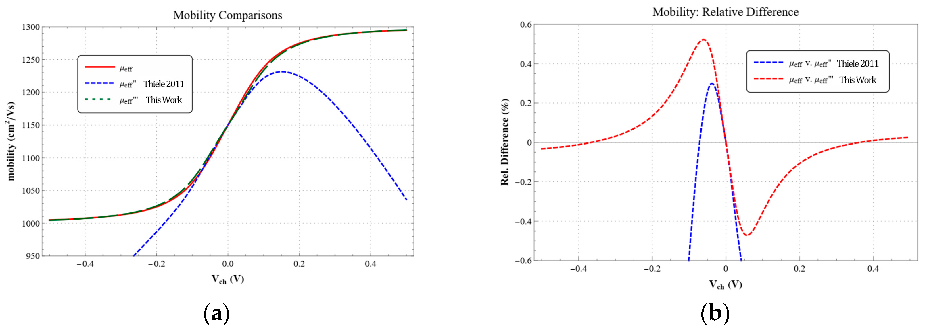
3.3. Simplifying the Effective Mobility for Simulation

The final step before populating (1) is to minimize the discrepancy of the effective mobility in Tian et al.’s model, which increases with the channel voltage (Figure 3) [10]. By considering the limit when the empirical parameter m is taken to infinity, the following expression for effective mobility is obtained:
μ e f f = lim x μ e f f = ( 14 z ( a + b V c h 2 ) a + b V c h 2 + n p u d V c h 1 + c V c h 2 + h ) ,
As shown in Figure 3, the improved effective mobility exhibits a higher degree of accuracy at high channel voltages, with the relative difference trending towards zero. Since m is simply an empirical fitting parameter, the impact on the accuracy of the model can be minimized. Moreover, using (16) to calculate effective mobility results in one less modeling parameter.

3.4. The Closed-Form Solution for the Drain Current

To arrive at a closed-form solution for the drain current I D S , (1) must be transformed to represent the channel voltage instead of the applied voltage. To achieve this, (11) may be integrated in terms of V c h , resulting in the following equation:
d V d V c h = 1 + d α min ( 2 + c V c h ( 3 + 2 c V c h 2 ) ) ( q + c V c h 2 ) 3 / 2
where d = 2 q 2 k B T ln ( 4 ) / ( C t + C b ) π ( v F ) 2 . I D S can then be solved in terms of V c h by substituting (17), (16), (7), (2), and (5) into (1) and performing the required integration. The integration for the IDS was performed in Mathematica supported by Rubi to aid in the integration process. The final equation for IDS comprises two terms; the first term represents the numerator, I D S n u m , and the second term represents the denominator, I D S d e n o m .
I D S n u m = W V c s V c d q ( a + b V c h 2 ) ( 1 + α min d ( 2 + c V c h 2 ( 3 + 2 c V c h 2 ) ) ( 1 + c V c h 2 ) 3 / 2 ) ( h + 14 z V c h 1 + c V c h 2 ) d V c h + W 0 V D S ( q n p u d h ) d V
I D S d e n o m = L + | V c d V c d 1 v F ( 1 + f V c h 2 e + g ( 1 + f V c h 2 ) ) ( h + 14 z ( a + V c h 2 ) a + b V c h 2 + n p u d V c h 1 + c V c h 2 + h α min ( 2 + c V c h 2 ( 3 + 2 c V c h 2 ) ) ( 1 + c V c h 2 ) 3 / 2 ) +
d α min ( 2 + c V c h 2 ( 3 + 2 c V c h 2 ) ) ( 1 + c V c h 2 ) 14 z V c h ( a + b V c h 2 ) a + b V c h 2 + n p u d d V c h |

4. The Implementation and Validation of the Model

The GFET model is implemented in Verilog-A, and Keysight’s ADS integrated Verilog-A compiler is used for the synthesis of the GFET and electrical characterization. We use the same method used in [9] to construct a two series-connected current branch model in Verilog-A by using the channel potential V c h and voltage drop V ( x ) as the model input parameters (node voltage) to represent the left- and right-hand sides of (12), showing the current through the node of the drain–channel potential and source-channel potential, respectively. The node voltage V c h at the source and drain derived from the current model is then used to calculate the Fermi velocity in (14). A novel biased-varying Fermi velocity model is realized using a similar method by creating two series-connected current branches representing the left- and right-hand sides of (14) and solving for the value of the carrier concentration, n, in the Fermi velocity calculation (Figure 4). A weighted average Fermi velocity vF is found based on the drain and source Fermi velocities and used to create the final Verilog-A model. Two sources of experimental data were used to validate the proposed enhanced GFET model: (1) published data for a dual-gated GFET from Wang et al. [21] and (2) a back-gated GFET obtained by authors from Graphenea Inc., Cambridge, MA, USA.

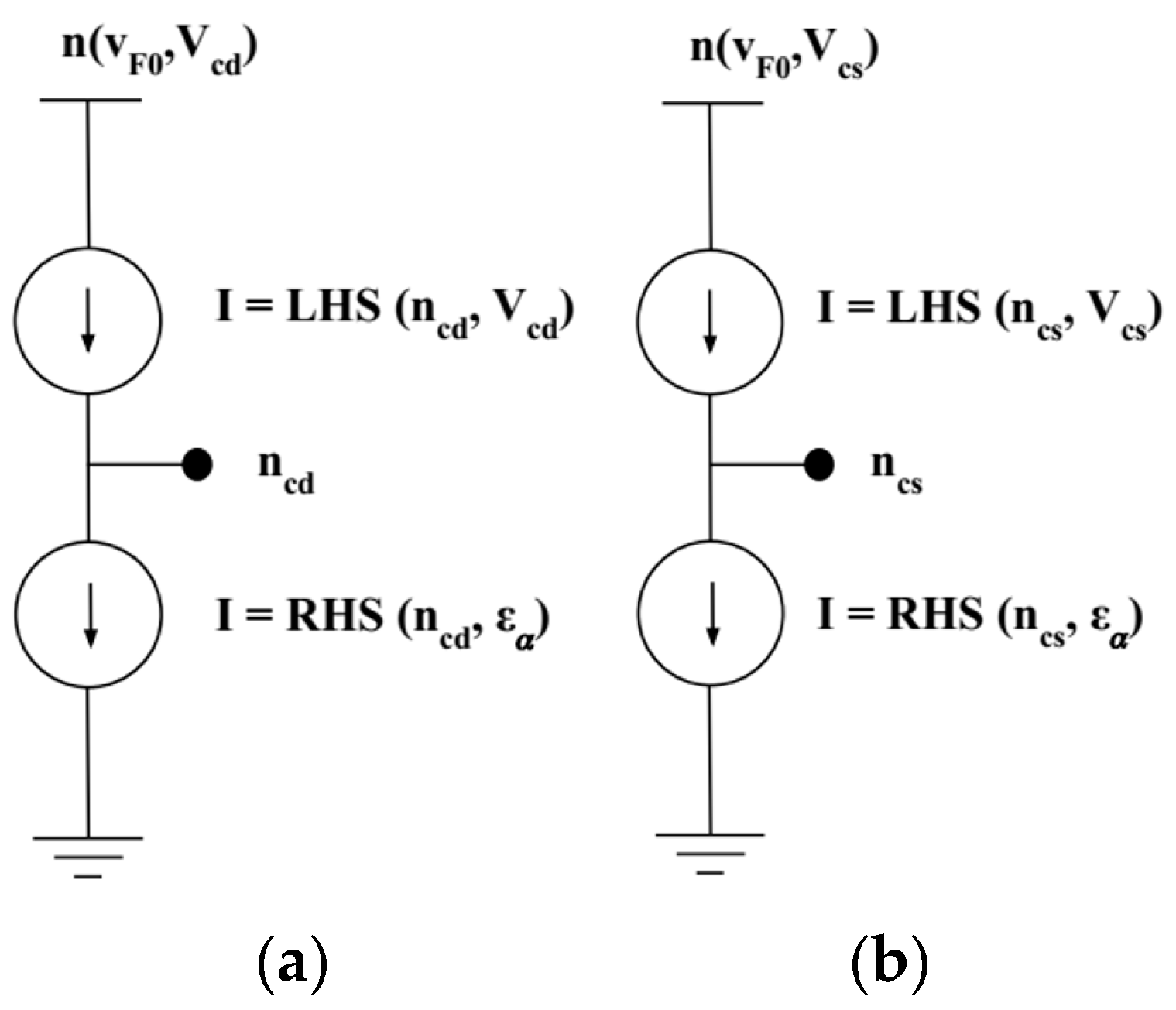
4.1. Creating the Enhanced GFET Model

To accurately find the IDS, two additional series resistors representing the drain and source contact resistances are added on either side of the drain–source current. This way, the channel voltage can be better estimated and used in the model to calculate the IDS. To simplify the model, the channel voltage is calculated using the ideal Fermi velocity. To achieve better DC convergence performance in solving the two current source methods for the Fermi velocity calculation in Equation (14), the Newton–Raphson method, an effective root-finding algorithm for root approximation in differential equations in Keysight’s ADS DC simulator, is used with large iteration steps when we apply the Verilog-A model in the circuit.

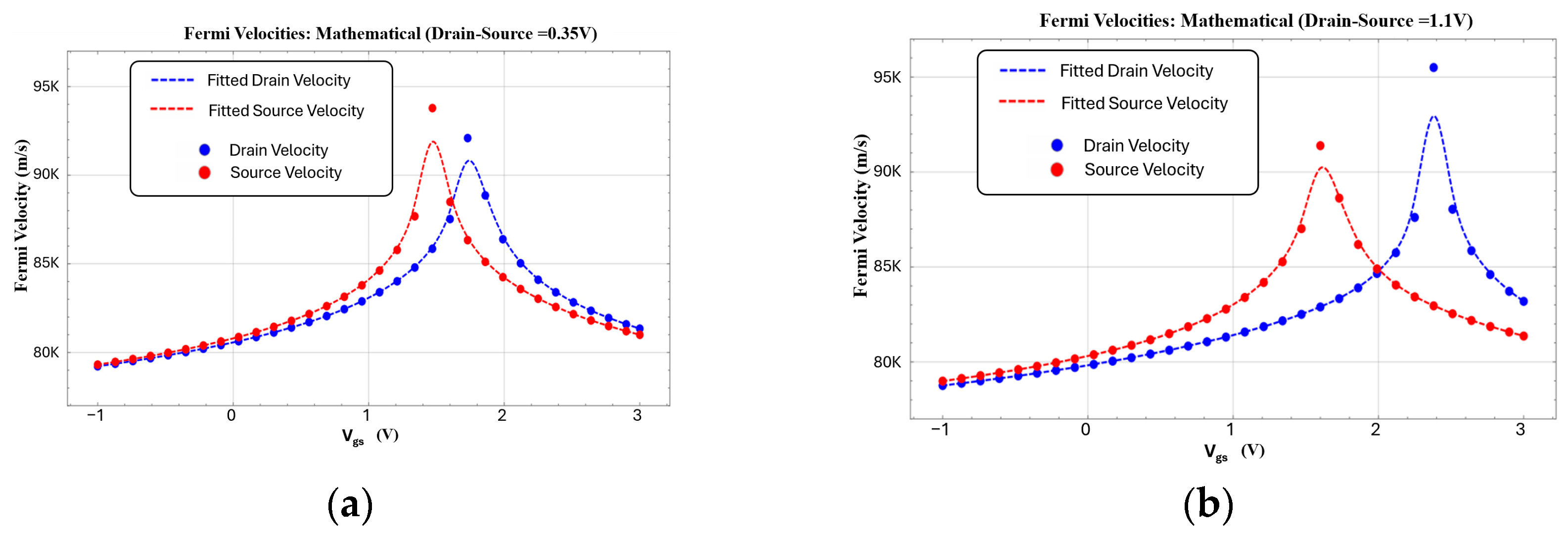
4.2. Fermi Velocity Model

Shown in Figure 5 are the extracted values of the Fermi velocities at the drain and source interfaces obtained from modeling Wang et al.’s device [21] using this work’s model and the parameters given in Wang et al.’s paper. The drain–source, VDS, values of 0.35 V (Figure 5a) and 1.1 V (Figure 5b) are chosen for this experiment. The blue dots and red dots represent the Fermi velocity of charge carriers at the drain and source, respectively. The fitted lines are b-splines of the data points for ease of viewing. Since the electron–electron interactions within the graphene drastically increase when the device is biased at the Dirac point, the effects of dielectric screening decrease [11,12], resulting in an increase in the Fermi velocity. As demonstrated in Figure 5, the Fermi velocity predicted by our model is in good agreement with the values obtained by Hwang et al. [12]. Moreover, the model exhibits the expected behavior for the Fermi velocity. Nevertheless, the proposed model shows a clear difference in the Fermi velocity at the drain and source of the channel with VGS basing, predicting the Fermi velocity more accurately across different bias points. However, using a single Fermi velocity value, calculated from (15), in the model limits the accuracy of the model.
As the difference between the drain and source channel voltages increases, the difference between the Fermi velocities at the source and drain increases (Figure 5). The method of Fermi velocity calculation found in (15) results in a weighted average of these two curves, causing an underestimation of the Fermi velocity around the true Dirac point at high channel voltages and at either extreme end of the graphs, which explains the increasing errors around the Dirac point.

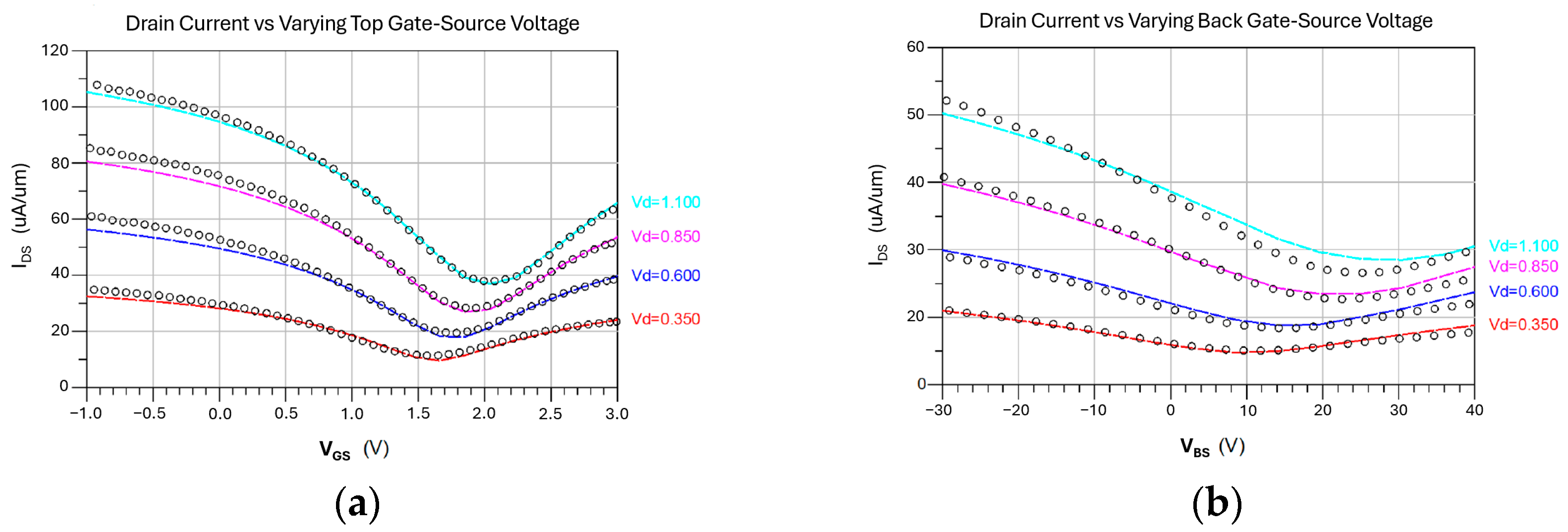
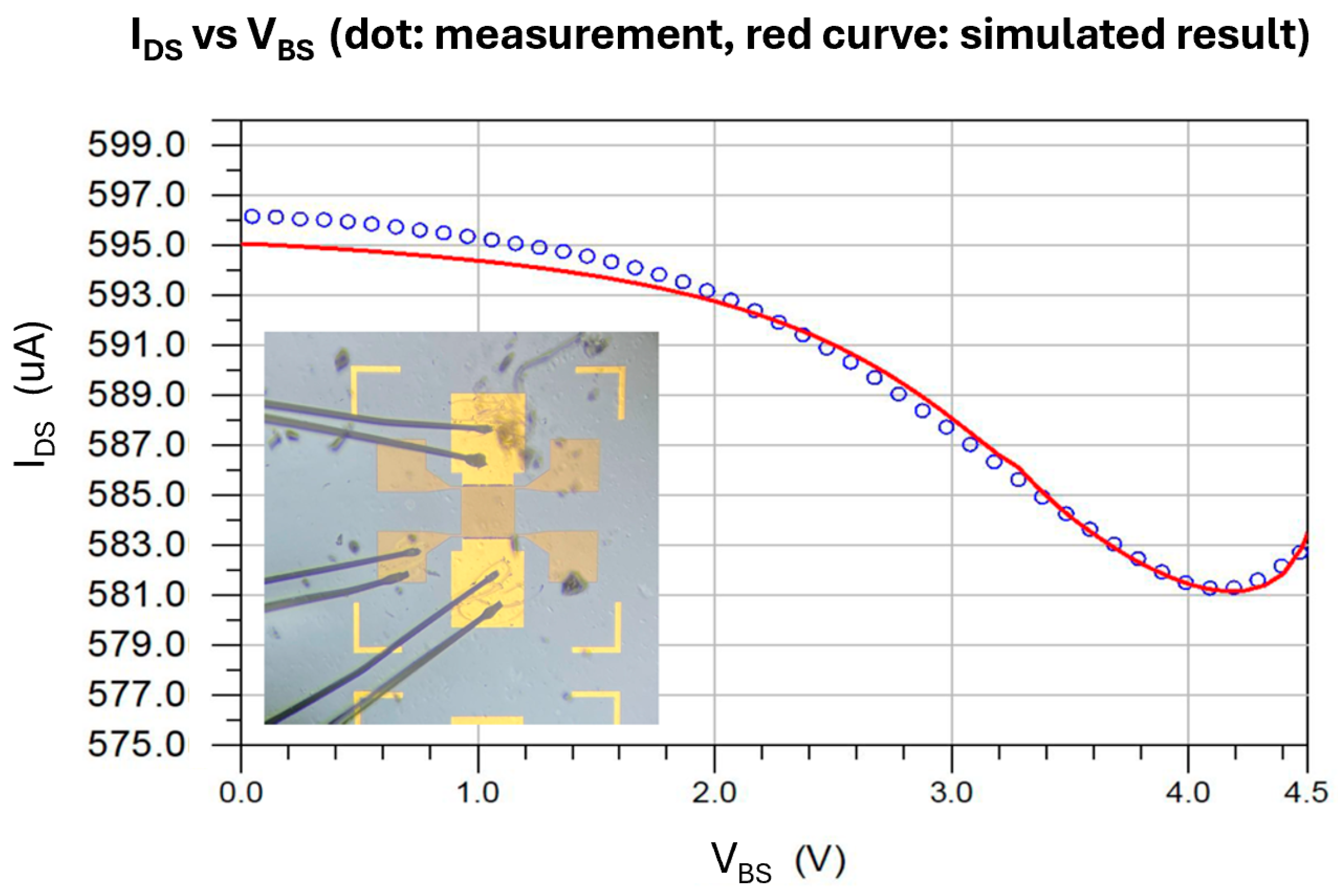
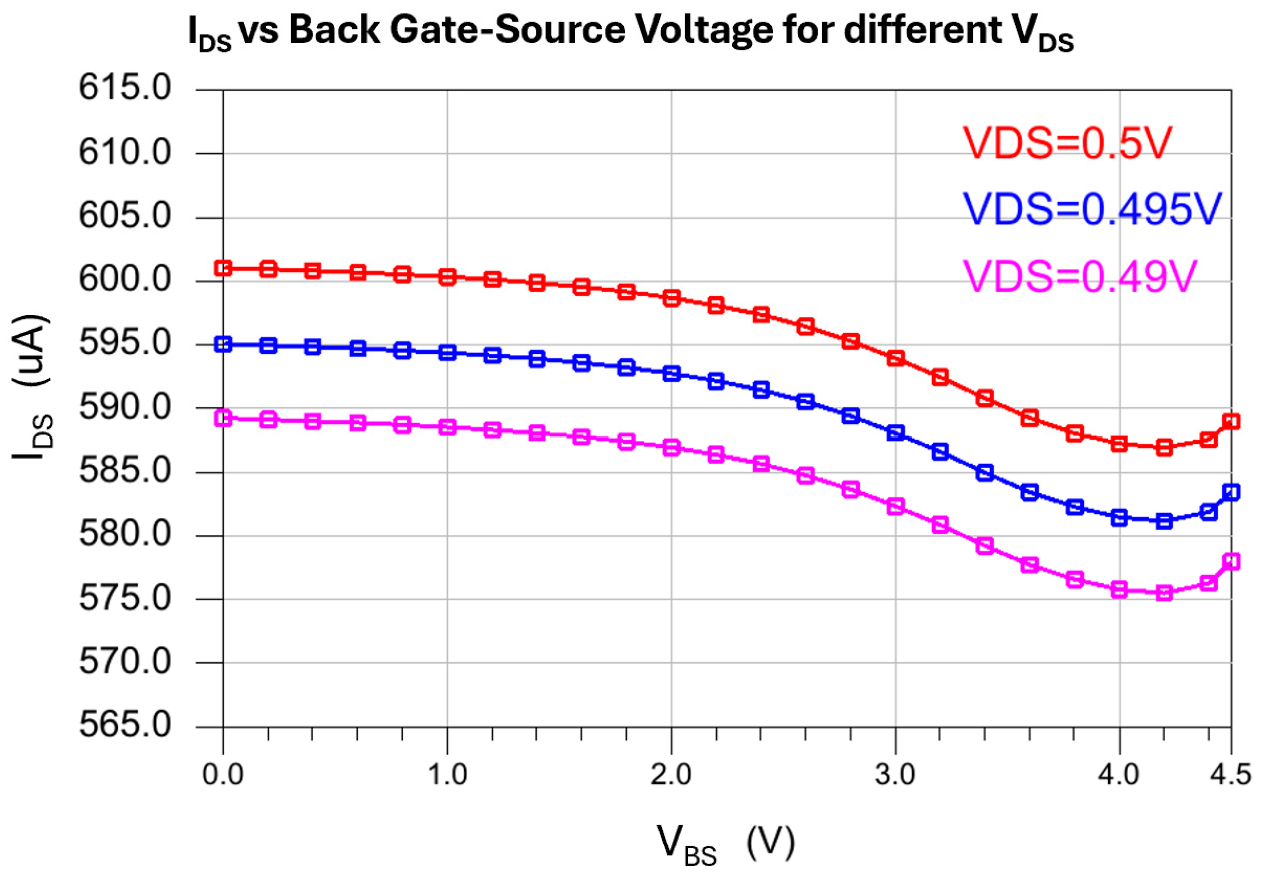
4.3. GFET Model Validation

Figure 6a presents the I-V characteristic of the dual-gated GFET from [21] using the proposed model when the top gate–source voltage is varied and the back gate is set to 0 V; the dotted plot shows the measured data from [21], while the solid line shows the simulation results. On the other hand, Figure 6b shows the I–V characteristics of the same device for various back gate–source voltages when the top gate–source voltage is set to 1.41 V. The device parameters used for this model are W = 25 µm, L = 5 µm, ε t = 9, ε b = 4, t o x t = 15 nm, t o x b = 300 nm, V g s 0 = 1.2 V, V b s 0 = 11 V, μ n = 920 cm 2 /Vs, μ p = 1330 cm 2 /Vs, ∆ = 90 m eV, T = 300 K, and R d = R s = 4.2 kΩ·µm. When comparing the results produced using our model with the published results of a dual-gated GFET measured by Wang et al. [21], a maximum relative difference of 8% is observed. Similarly, the I–V characteristics of a back-gated GFET provided by Graphenea Inc. are modeled and compared with the measurement results (Figure 7). The dotted curve shows the measurement results, while the red solid curve presents the simulated results obtained using the proposed GFET model. The device parameters used for this model are W = 100 µm, L = 100 µm, ε t = 1, ε b = 9.34, t o x t = 5 nm, t o x b = 300 nm, V g s 0 = 0 V, V b s 0 = 3.1 V, μ n = 570 cm 2 /Vs, μ p = 650 cm 2 /Vs, ∆ = 80 m eV, T = 300 K, and R d = R s = 30 kΩ·µm. The back gate voltage,VBS, increases from 0 V to 4.5 V, while the drain–source voltage, VDS, is kept near 0.5 V. Compared to the measured results, the modeled IDS shows a maximum relative difference smaller than ±1%. Despite improved accuracy, the model generally underestimates IDS, except near the Dirac point, where the model slightly overestimates IDS. This small error is the consequence of the method used to calculate a singular Fermi velocity value. This model accuracy can be improved by considering the uneven distribution of the fermi velocity from drain to source at such biasing condition and perform more iterations to better estimate the weighted average v F  throughout channel. Nevertheless, the accuracy demonstrated by our model is comparable if not better than those obtained by applying other GFET models. Another consequence of the concessions made to create the proposed Fermi velocity model is using the ideal value of the Fermi velocity to calculate the channel voltage in (12). This assumption resulted in a potential uneven distribution of the Fermi velocity variation from the source to drain. To show the robustness of the proposed model for various channel current and drain–source voltages, the IDS and VDS vs. the back gate source voltage was simulated (Figure 8). Figure 8 shows IDS vs. the back gate–source voltage (VBS) when VDS changes from 0.49 V to 0.50 V. The plots show the same trend and behavior as those shown in Figure 6, indicating good accuracy in modeling IDS for different VDS, making the model useful for a variety of analog electronic circuit design applications. Due to the lack of access to short-channel GFET devices, model validation is only carried out on long-channel devices. Recognizing the non-idealities affecting the performance of the short-channel GFET devices (e.g., velocity saturation), further improvement, particularly in the weighted average estimation of the Fermi velocity at the drain and source, may be necessary.

5. Conclusions

A novel Verilog-A GFET model which uses a closed-form solution to determine the Fermi velocity is developed and evaluated. A systematic analysis of existing GFET models is performed to identify a methodology to accurately determine the Fermi velocity for various gate–source voltages. Using this information, a mathematical model which relates the Fermi velocity to the graphene carrier concentration, channel voltage, and dielectric constants of the gates is developed. During this process, a weighted averaging method is used to calculate a single value for the Fermi velocity. The accuracy of the model to predict the Fermi velocity as influenced by the top and bottom gate substrates is verified using experimental data from dual-gated and back-gated GFETs. The drain current measurement results differ by less than 8% at a single point and can be within ±1% of the measured values for long-channel devices produced by Graphenea, verifying the accuracy of this model for GFET-based circuit designs.

Author Contributions

Conceptualization, J.M.; Software, S.J. and J.M.; Validation, P.K.; Formal analysis, S.J. and J.M.; Investigation, J.M.; Resources, H.M.L.; Writing—original draft, J.M.; Writing—review & editing, S.J., M.C.S., C.Z. and H.M.L.; Funding acquisition, H.M.L. All authors have read and agreed to the published version of the manuscript.

Funding

This research is partially funded by the U.S. National Science Foundation (NSF) under grant No. 2221925.

Data Availability Statement

Data are contained within the article.

Conflicts of Interest

The authors declare no conflict of interest.

References

  1. Novoselov, K.S.; Geim, A.K.; Morozov, S.V.; Jiang, D.; Zhang, Y.; Dubonos, S.V.; Grigorieva, I.V.; Firsov, A.A. Electric field effect in atomically thin carbon films. Science 2004, 306, 666–669. [Google Scholar] [CrossRef] [PubMed]
  2. Thiele, S.A.; Schaefer, J.A.; Schwierz, F. Modeling of graphene metal-oxide-semiconductor field-effect transistors with gapless large-area graphene channels. J. Appl. Phys. 2010, 107, 094505. [Google Scholar] [CrossRef]
  3. Tian, J. Theory, Modelling and Implementation of Graphene Field- Effect Transistor. Ph.D. Thesis, Queen Mary University of London, London, UK, 2017. [Google Scholar]
  4. Fang, T.; Konar, A.; Xing, H.; Jena, D. Carrier statistics and quantum capacitance of graphene sheets and ribbons. Appl. Phys. Lett. 2007, 91, 0921091-1–0921091-3. [Google Scholar] [CrossRef]
  5. Thiele, S.; Schwierz, F. Modeling of the steady state characteristics of large-area graphene field-effect transistors. J. Appl. Phys. 2011, 110. [Google Scholar] [CrossRef]
  6. Wang, Z.; Zhang, Z.; Peng, L. Graphene-based ambipolar electronics for radio frequency applications. Chin. Sci. Bull. 2012, 57, 2956–2970. [Google Scholar] [CrossRef]
  7. Parrish, K.; Ramón, M.E.; Banerjee, S.; Akinwande, D. A Compact Model for Graphene FETs for Linear and Non-linear Circuits. In Proceedings of the IEEE International Conference on Simulation of Semiconductor Processes and Devices, Denver, CO, USA, 5–7 September 2012. [Google Scholar]
  8. Rodriguez, S.; Vaziri, S.; Smith, A.; Fregonese, S.; Ostling, M.; Lemme, M.C.; Rusu, A. A Comprehensive Graphene FET Model for Circuit Design. IEEE Trans. Electron Devices 2014, 61, 1199–1206. [Google Scholar] [CrossRef]
  9. Landauer, G.M.; Jimenez, D.; Gonzalez, J.L. An Accurate and Verilog-A Compatible Compact Model for Graphene Field-Effect Transistors. IEEE Trans. Nanotechnol. 2014, 13, 895–904. [Google Scholar] [CrossRef]
  10. Tian, J.; Katsounaros, A.; Smith, D.; Hao, Y. Graphene Field-Effect Transistor Model with Improved Carrier Mobility Analysis. IEEE Trans. Electron Devices 2015, 62, 3433–3440. [Google Scholar] [CrossRef]
  11. Elias, D.C.; Gorbachev, R.V.; Mayorov, A.S.; Morozov, S.V.; Zhukov, A.A.; Blake, P.; Ponomarenko, L.A.; Grigorieva, I.V.; Novoselov, K.S.; Guinea, F.; et al. Dirac cones reshaped by interaction effects in suspended graphene. Nat. Phys. 2011, 7, 701–704, Erratum in: Nat. Phys. 2012, 7, 172. [Google Scholar] [CrossRef]
  12. Hwang, C.; Siegel, D.A.; Mo, S.-K.; Regan, W.; Ismach, A.; Zhang, Y.; Zettl, A.; Lanzara, A. Fermi velocity engineering in graphene by substrate modification. Sci. Rep. 2012, 2, 590. [Google Scholar] [CrossRef]
  13. Van Halen, P.; Pulfrey, D.L. Accurate, short series approximations to Fermi–Dirac integrals of order −1/2, 1/2, 1, 3/2, 2, 5/2, 3, and 7/2. J. Appl. Phys. 1985, 57, 5271–5274. [Google Scholar] [CrossRef]
  14. Zhu, W.; Perebeinos, V.; Freitag, M.; Avouris, P. Carrier scattering, mobilities, and electrostatic potential in monolayer, bilayer, and trilayer graphene. Phys. Rev. B 2009, 80, 235402. [Google Scholar] [CrossRef]
  15. Luryi, S. Quantum capacitance devices. Appl. Phys. Lett. 1988, 52, 501–503. [Google Scholar] [CrossRef]
  16. Parrish, K.N.; Akinwande, D. Impact of contact resistance on the transconductance and linearity of graphene transistors. Appl. Phys. Lett. 2011, 98, 183505. [Google Scholar] [CrossRef]
  17. Deng, J.; Wong, H.-S.P. A Compact SPICE Model for Carbon-Nanotube Field-Effect Transistors Including Nonidealities and Its Application—Part I: Model of the Intrinsic Channel Region. IEEE Trans. Electron Devices 2007, 54, 3186–3194. [Google Scholar] [CrossRef]
  18. Whelan, P.R.; Shen, Q.; Zhou, B.; Serrano, I.G.; Kamalakar, M.V.; A Mackenzie, D.M.; Ji, J.; Huang, D.; Shi, H.; Luo, D.; et al. Fermi velocity renormalization in graphene probed by terahertz time-domain spectroscopy. 2D Mater. 2020, 7, 035009. [Google Scholar] [CrossRef]
  19. Stauber, T.; Parida, P.; Trushin, M.; Ulybyshev, M.V.; Boyda, D.L.; Schliemann, J. Interacting Electrons in Graphene: Fermi Velocity Renormalization and Optical Response. Phys. Rev. Lett. 2017, 118, 266801. [Google Scholar] [CrossRef] [PubMed]
  20. Aguirre-Morales, J.-D.; Fregonese, S.; Mukherjee, C.; Wei, W.; Happy, H.; Maneux, C.; Zimmer, T. A Large-Signal Monolayer Graphene Field-Effect Transistor Compact Model for RF-Circuit Applications. IEEE Trans. Electron Devices 2017, 64, 4302–4309. [Google Scholar] [CrossRef]
  21. Wang, H.; Hsu, A.; Kong, J.; Antoniadis, A.D.; Palacios, T. Compact Virtual-Source Current–Voltage Model for Top- and Back-Gated Graphene Field-Effect Transistors. IEEE Trans. Electron Devices 2011, 58, 1523–1533. [Google Scholar] [CrossRef]
Figure 1. The equivalent circuit model used to solve for the Fermi velocity and (a,b) to solve for the carrier concentration of the channel at the drain and source, respectively.
Electronics 13 05051 g001
Figure 2. Schematic diagrams of the voltage bias states in a GFET: (a) electron conduction, (b,c) ambipolar conduction with opposite channel voltage bias, and (d) hole conduction. The images were adapted from [20].
Electronics 13 05051 g002
Figure 3. (a) A comparison of the proposed effective mobility approximation with prior work and the actual mobility and (b) the relative difference between the actual mobility and the mobility estimated using the two models (new and old) [5].
Electronics 13 05051 g003
Figure 4. A circuit diagram of the proposed small-signal model of the GFET using current sources influenced by Vch and the averaged Fermi velocity vF varied by top and back gate biasing voltages. The contact resistance and parasitic capacitance are also shown.
Electronics 13 05051 g004
Figure 5. Simulated drain and source Fermi velocity values for drain source voltage at (a) 0.35 V and (b) 1.1 V using this work’s model with input data from Han Wang et al.’s device [21].
Electronics 13 05051 g005
Figure 6. Comparison of simulated I-V characteristics to measurement data from Wang et al. [21]. (a) I–V characteristics with constant VGS; (b) I–V characteristics with constant VBS.
Electronics 13 05051 g006
Figure 7. A comparison of the IDS vs. VBS model with the measured results from Graphenea’s GFET.
Electronics 13 05051 g007
Figure 8. Simulation of IDS vs. VBS when VDS varies from 0. 49 V to 0.50 V.
Electronics 13 05051 g008
Disclaimer/Publisher’s Note: The statements, opinions and data contained in all publications are solely those of the individual author(s) and contributor(s) and not of MDPI and/or the editor(s). MDPI and/or the editor(s) disclaim responsibility for any injury to people or property resulting from any ideas, methods, instructions or products referred to in the content.

