Abstract
Understanding the behavior of p-n junctions is fundamental in semiconductor physics and electronics engineering. Traditional teaching methods often focus on material-based definitions of p-type and n-type semiconductors by discussing doping. However, within the depletion region, an additional description is also applicable; this relates to the relative positioning of the energy, which depends on the energy discrepancy between the Fermi and intrinsic Fermi levels and is also based on carrier type. These two descriptions are at variance when describing the properties of the voltage drop and the energy band bending in the depletion regions of the p-n junction diode in equilibrium, and also when the doping is asymmetrical ). Our experience teaching introductory semiconductor courses has revealed a lack of clarity regarding the behavior of the region types within the depletion region, which can, in turn, lead to confusion and hinder students’ understanding of the critical concept of voltage drop in the depletion region. This paper aims to underline the difference between the two descriptions above and propose specific terminology for the energy band-based definition in the depletion region; we suggest that instead of “n-type” and “p-type”, the terms “n-like” and “p-like” materials will be used. Further, building on the similarities in energy band bending and potential variations between p-n junctions and MOS capacitors, we suggest that studying the depletion region of p-n junctions can offer valuable insights into the formation and behavior of the inversion layer at the semiconductor surface of MOS capacitors.
1. Introduction
The basic theory of ideal p-n junctions in equilibrium treats the space charge region (SCR), or the depletion region, under the assumptions that (i) the junction is abrupt and (ii) the junction is depleted of free electrons and hole carriers, by neglecting the carrier concentration in the depletion region. In addition, the regions outside the SCR are assumed to be quasi-neutral with local charge neutrality and a zero electrical field [1,2,3,4,5,6].
Fundamental academic courses on semiconductors primarily analyze symmetrically doped p-n junctions. The junctions are created structurally at the contact between the p- and n-type materials, which is the same as the junction created by the depletion regions. The metallurgical junction is at . However, for abrupt, asymmetrical p-n junctions, where , additional terminology can be helpful when analyzing the behavior within the depletion region. In this work, we propose adopting terms like “junction-like”, “p-like”, and “n-like” within the depletion region based on the position of the Fermi level () relative to the intrinsic level (), or based on the majority carrier type. The “junction-like” feature created within the depletion region is when the electron and hole concentrations are equal, or when and are equal at . The “p-like” and “n-like” terminology refers to the regions in the depletion layer where the distance between and is negative and positive, respectively. Some lecturers use the term “intrinsic point” instead of “junction-like” at .
In most university curricula, the teaching of MOS capacitors typically follows that of p-n diodes. This sequence encourages students to build upon their understanding of basic semiconductor devices before introducing the more complex concepts associated with MOS structures. Three key terms are essential when discussing MOS capacitors: accumulation, depletion, and inversion. Inversion refers to the phenomenon where an external voltage applied to the gate electrode repels the majority carrier type away from the surface and attracts the minority carriers toward the surface, effectively creating a thin layer of opposite-type carriers. For example, in a p-type substrate, applying a positive voltage to the gate would induce an inversion layer rich in electrons (n-type). This behavior is analogous to the concept of “n-like” regions. Therefore, the proposed terminology will also be useful when studying MOS capacitors.
In this paper, we assume that the diode is in equilibrium, since the total electron and hole net current is zero. It is reasonable to assume that the energy is approximately constant and appears on an energy diagram (Figure 1) as a horizontal line through all the diode structures, including in the depletion region.
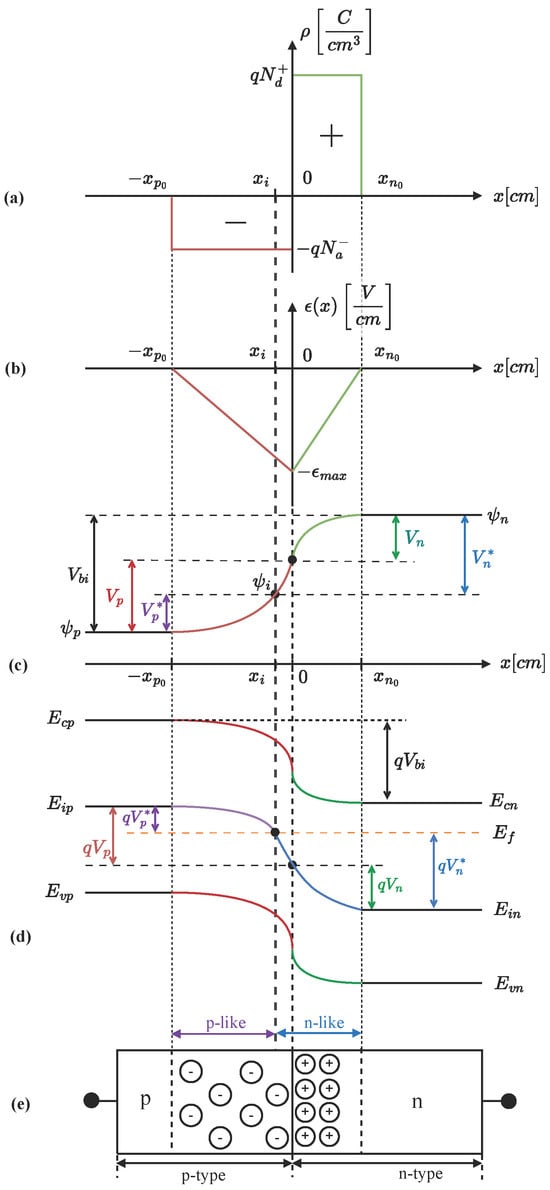
Figure 1.
Ideal p-n junction: (a) charge density distribution, (b) electrical field distribution, (c) potential distribution, (d) energy band diagram, (e) structure of the ideal p-n junction.
2. The Structural Junction Model
The structural junction model is mainly used for finding the properties of the charge distribution , the electric field , the potential distribution , and the energy diagram. The physical “p-/n-like” junction model is used to find the properties of the built-in voltage and the energy band bending.
The two p and n depletion regions (the SCR) appear on the two sides of the diode junction. We can derive the charge distribution under two basic assumptions of an ideal diode: (i) the junction is abrupt and (ii) the free electron and hole carrier concentrations are neglected. By applying Poisson’s equation, we can derive the electric field and potential distribution , as described in Equations (1)–(3) and shown in Figure 1a–c, for the case of :
At p depletion regions, where ,
At n depletion regions, where ,
Note that the structural junction is at , and the potentials and are floating. Due to the net negative and positive charges in the p- and n-side depletion regions, the potential curve is concave-up and -down, respectively.
The voltage drop on the p and n depletion regions, given in Equations (4a) and (4b), are obtained by calculating the area under the triangle curve of the electric field (see also Figure 1b) [4,5,6]:
where
The energy diagram is shown in Figure 1d and obtained using the relation between the conduction energy, the potential energy , and the electron potential , as given in Equation (6):
3. The Physical “p-/n-like” Junction Model
In this model, the “p-like” region is defined as the case where the concentration of holes is higher than that of electrons () and where . Conversely, for the “n-like” region, and . The “junction-like” feature will be at , where . However, at the structural junction (at ), , i.e., the region where , is called the “inversion region”, a term commonly used in MOS capacitors. The hole and electron concentrations can be expressed as a function of the distance between and , given in Equations (7a) and (7b):
The voltage drops on the “p-like” and “n-like” regions at and , respectively, and the built-in voltages are given in Equations (8a), (8b), and (8c), respectively:
Note, in the case of , the voltage drop on the p or n depletion regions (Equations (4a) and (4b)) is not the same as the voltage drop on “p-/n-like” depletion regions (Equations (8a) and (8b)). However, when teaching p-n diode properties in most undergraduate courses, one deals with the case where , and in this case, the voltage drop on the p or n depletion regions is the same as the voltage drop on the “p-/n-like” depletion regions.
We now present a numerical example. For the Si p-n junction, we consider three cases: one with asymmetric doping and two with symmetric doping. For all the cases, cm−3. Given the values of and , the voltage drop values are calculated as follows:
Therefore, in the case of , students may erroneously use the majority material doping model instead of the energy-related model.
The physical model of p-n junctions can also be beneficial when studying MOS capacitors. The principles of band bending and the properties of the depletion region are quite similar for both p-n junctions and MOS capacitors. Additionally, MOS capacitors in inversion mode may also have “n-like” or “p-like” regions.
For instance, in a p-type substrate of a MOS capacitor, applying a sufficiently large positive gate voltage can invert a portion of the substrate near the surface from p-type to n-type due to electron accumulation, thus forming an “n-like” region. In this inverted area, a larger negative charge exists, comprising both negative acceptor ions and electrons. The band bending is such that the level at the surface is now below the level, resulting in the formation of the “n-like” region. The provided discussion may also be beneficial for advanced topics, such as the study of complex Schottky barrier formations [7]; an in-depth discussion of such topics is beyond the scope of our publication.
It may be advisable to delay the introduction of this more complex case in an introductory to an advanced semiconductor course, where a deeper level of analysis is required. Another reported approach is to utilize simulation-based methods [8,9,10,11]. Implementing simulations can simplify complex concepts, enhance comprehension of the studied material, and reduce students’ misconceptions [12].
4. Summary
In this paper, we defined three new terms: “junction-like”, “p-like”, and “n-like” depletion regions of p-n diodes and underlined the differences between the two descriptions of n/p types and “n/p-like” types. We showed that for an abrupt junction and when , the voltage drops on the p-type () and “p-like” () within the depletion regions are not the same, where
The same can be obtained for n-types and “n-like” types within the depletion region.
For the conventional case of symmetrical doping, , there is no discrepancy between the two definitions.
Author Contributions
Conceptualization, D.B., S.H. and M.Z.; writing—original draft preparation, S.H. and M.Z.; writing—review and editing, D.B. All authors have read and agreed to the published version of the manuscript.
Funding
This research received no external funding.
Data Availability Statement
No new data were created or analyzed in this study. Data sharing is not applicable.
Conflicts of Interest
The authors declare no conflicts of interest.
References
- Mazhari, B.; Mahajan, A. An Improved Interpretation of Depletion Approximation in p-n-Junctions. IEEE Trans. Educ. 2005, 48, 60–62. [Google Scholar] [CrossRef]
- Sze, S.M.; Ng, K.K. Physics of Semiconductor Devices, 3rd ed.; Wiley: Hoboken, NJ, USA, 2006. [Google Scholar]
- De Wiele, F.V.; Demoulin, E. Inversion layers in abrupt p-n junctions. Solid-State Electron. 1970, 13, 717–726. [Google Scholar] [CrossRef]
- Pierret, R.F. Semiconductor Fundamentals: Volume I, 2nd ed.; Pearson: Reading, MA, USA, 1989. [Google Scholar]
- Neamen, D.A. Semiconductor Physics and Devices, 4th ed.; McGraw-Hill Higher Education: New York, NY, USA, 2012. [Google Scholar]
- Streetman, B.; Banerjee, S. Solid State Electronic Devices, 7th ed.; Pearson Higher Education: London, UK, 2015. [Google Scholar]
- Mendoza-Sánchez, A.R.; Hernández-Rodríguez, Y.; Casas-Espínola, J.; Cigarroa-Mayorga, O. Nanostructural modulation of Schottky barrier in Au/α-MoO3 heterojunction via Au nanoparticle size control. Appl. Surf. Sci. 2024, 670, 160624. [Google Scholar] [CrossRef]
- Narayanan, M.; Al-Nashash, H. Introducing undergraduate students to simulation of semiconductor doping techniques. Comput. Electr. Eng. 2009, 35, 567–577. [Google Scholar] [CrossRef]
- Alnassar, M.S.N. Utilization of open-source software in teaching the physics of P-N diodes. Comput. Appl. Eng. Educ. 2023, 31, 867–883. [Google Scholar] [CrossRef]
- Liang, J. A study to analyze the importance of establishing a mathematical model for teaching college physics. Appl. Math. Nonlinear Sci. 2023, 9, 1–16. [Google Scholar] [CrossRef]
- Yang, X.; Schroder, D.K. Some Semiconductor Device Physics Considerations and Clarifications. IEEE Trans. Electron Devices 2012, 59, 1993–1996. [Google Scholar] [CrossRef]
- Nelson, K.G.; McKenna, A.F.; Brem, S.K.; Hilpert, J.; Husman, J.; Pettinato, E. Students’ Misconceptions about Semiconductors and Use of Knowledge in Simulations. J. Eng. Educ. 2017, 106, 218–244. [Google Scholar] [CrossRef]
Disclaimer/Publisher’s Note: The statements, opinions and data contained in all publications are solely those of the individual author(s) and contributor(s) and not of MDPI and/or the editor(s). MDPI and/or the editor(s) disclaim responsibility for any injury to people or property resulting from any ideas, methods, instructions or products referred to in the content. |
© 2024 by the authors. Licensee MDPI, Basel, Switzerland. This article is an open access article distributed under the terms and conditions of the Creative Commons Attribution (CC BY) license (https://creativecommons.org/licenses/by/4.0/).