Article

High-Data-Rate Modulators Based on Graphene Transistors: Device Circuit Co-Design Proposals †

by
Anibal Pacheco-Sanchez
1,2,*,‡,
J. Noé Ramos-Silva
3,‡,
Nikolaos Mavredakis
1,
Eloy Ramírez-García
3 and
David Jiménez
1
1
Departament d’Enginyeria Electrònica, Escola d’Enginyeria, Universitat Autònoma de Barcelona, 08193 Barcelona, Spain
2
Departamento de Electrónica y Tecnología de Computadores, Universidad de Granada, 18011 Granada, Spain
3
UPALM, Edif. Z-4 3er Piso, Instituto Politécnico Nacional, Mexico City 07738, Mexico
*
Author to whom correspondence should be addressed.
This paper is an extended version of our paper published in Pacheco-Sanchez, A.; Ramos-Silva, J.N.; Mavredakis, N.; Ramírez-García, E.; Jiménez, D. Design of GFET-based active modulators leveraging device performance reproducibility conditions. In Proceedings of the IEEE Conference on Design of Circuits and Integrated Systems (DCIS), Malaga, Spain, 15–17 November 2023.
These authors contributed equally to this work.
Electronics 2024, 13(20), 4022; https://doi.org/10.3390/electronics13204022
Submission received: 15 September 2024 / Revised: 10 October 2024 / Accepted: 11 October 2024 / Published: 12 October 2024

Abstract

:
The multifunctionality feature of graphene field-effect transistors (GFETs) is exploited here to design circuit building blocks of high-data-rate modulators by using a physics-based compact model. Educated device performance projections are obtained with the experimentally calibrated model and used to choose an appropriate improved feasible GFET for these applications. Phase-shift and frequency-shift keying (PSK and FSK) modulation schemes are obtained with 0.6   G Hz GFET-based multifunctional circuits used alternatively in different operation modes: inverting and in-phase amplification and frequency multiplication. An adequate baseband signal applied to the transistors’ input also serves to enhance the device and circuit performance reproducibility since the impact of traps is diminished. Quadrature PSK is also achieved by combining two GFET-based multifunctional circuits. This device circuit co-design proposal intends to boost the heterogeneous implementation of graphene devices with incumbent technologies into a single chip: the baseband pulses can be generated with CMOS technology as a front end of line and the multifunctional GFET-based circuits as a back end of line.

1. Introduction

In any wire-based and wireless communication system, the message sent by a transmitter from one end and delivered to a receiver at the other end consists of controlled changes in electrical signal characteristics such as amplitude, frequency and phase. This process is known as modulation and requires a sinusoidal radiofrequency (RF) carrier signal and a baseband signal. The former is the one to be modified and the latter the modifier, which can be either analog (sinusoidal) or digital (pulse). The type of modulation process is defined according to the modified signal characteristic. Each type of modulation has its proper advantages and disadvantages over other ones; however, one of the most attractive features of digital modulation is the fact that the digital symbols (bits) within the baseband signal are not required to be reconstructed by the receiver, and hence, a message can be properly transmitted with predefined symbol combinations and appropriate decision thresholds [1].
For the three basic digital modulation schemes, i.e., amplitude-shift keying (ASK), frequency-shift keying (FSK) and phase-shift keying (PSK), the linear and nonlinear regions of devices, e.g., diodes, varactors and transistors, are exploited depending on the desired outcome [1,2]. However, it is difficult to find modulators using a single incumbent device switching between its linear and nonlinear bias regions for digital modulation purposes. This is related to the high asymmetry between such regions (see, e.g., the transfer characteristic of a unipolar silicon transistor), which limits the swing of the RF signal and/or the amplifying capabilities. Such a constraint impacts the power consumption and chip area of the circuits. Ambipolar transistors can alleviate the modulators’ design since their linear regimes—in their transfer characteristic—are quasi-symmetrical with respect to a nonlinear region defined by a charge neutrality point [3].
Emerging field-effect transistors (FETs) with low-dimensional channel materials, such as carbon nanotubes (CNTs), nanowires (NWs), two-dimensional (2D) transition metal dichalcogenides (TMDs) and graphene (G), are ambipolar devices either by their inherent physical mechanisms or are enhanced by controlled electrical doping [4,5,6,7]. Fabrication efforts have focused on exploiting either the linear or the nonlinear regions of CNTFETs separately for RF amplifiers or frequency conversion, respectively, [8]. Only modeling-based device circuit co-design efforts have been proposed to improve the dynamic performance of such circuits by exploiting both the device linear and nonlinear regimes and to use them as building blocks for high-data-rate modulators [9]. On the other hand, TMD-based FET digital modulators have been demonstrated recently for a frequency of operation within the k Hz range by using MoTe2 as the transistor channel [6]. In addition to the low-frequency operation, the existence of a bandgap in MoTe2 induces a minimum static drain current of a few n A and an extremely low output dynamic signal (tens of n A ). The latter questions the practical application of such modulators due to the signal being in a range similar to the noise floor of instruments and amplifiers. Regarding radiofrequency modulators based on GFETs, there have been some proof-of-concept demonstrations working within the k Hz range and using one single device but without any circuit design strategies for improving matching and/or stability conditions [10,11]. The only G Hz modulators based on any emerging technology have been demonstrated with GFETs in [12] (on–off keying at 96 G Hz ) and [13] (ASK and PSK at 90 G Hz ) obtained with zero-bias device conditions, i.e., V DS = 0 . Hence, these pure resistive GFET-based designs exploit the inherent high mobility of the graphene channel but yield a poor performance in terms of output power due to the lack of gain.
RF circuit applications based on emerging FET technologies, such as the high-data-rate modulators discussed above, have been demonstrated [14] in order to find suitable niches for these novel devices. However, an issue that still needs to be tackled toward the successful adoption of these technologies is their reproducibility at both device (the DC and AC performance) and circuit levels [15,16,17]. One of the main sources of low device (and hence circuit) reproducibility in these transistors is the high density of defects and traps inherent to the high- κ gate dielectric [18] that all of them use. From the characterization point of view, it is possible to reduce the impact of traps on the device performance, i.e., to improve their reproducibility, by applying suitable bias schemes [16,17]. One of these techniques involves alternating the DC gate biasing by pulses of different polarities [16]. This technique is proposed here and is suggested to be provided by a CMOS platform, combining in a heterogeneous circuit a GFET in the back end of line (BEOL) and silicon devices in the front end of line [19,20]. Furthermore, the opposing-pulse biasing scheme can be exploited not only at a device level but also for circuit applications since such a biasing sequence can be used as a baseband digital signal for modulators: overcoming reproducibility issues at the same time as proposing new niches for emerging devices such as GFETs.
In this work, discussions of active GFET-based modulators presented in [21,22] have been extended to a different operation frequency, i.e., 0.6   G Hz , and to the proposal of FSK modulation achieved with one single graphene transistor. A general discussion on how the inherent ambipolarity of GFETs enhances their multifunctionality is provided in Section 2. The calibration and optimization of the physics-based compact GFET model are discussed in Section 3. The designs of multifunctional circuits based on GFETs and the results of the three operation modes are shown in Section 4. PSK, FSK and QPSK modulators based on multifunctional GFET circuits are discussed in Section 5. A conclusion is provided in Section 6.

2. Exploiting Ambipolarity in GFETs

In contrast to traditional transistors, the charge is never depleted in GFETs as a consequence of the gapless feature of this two-dimensional material, which enhances their ambipolarity operation. The transfer characteristic of ambipolar transistors has two distinct quasi-linear operation modes in which either holes or electrons dominate the transport, hence resembling classical p-type (negative transconductance g m = I D / V GS ) and n-type (positive g m ) FETs [3], as shown in Figure 1 (the top-left panel). These operation regimes are separated by a high nonlinear region where the minimum current level is obtained at the charge neutrality point, identified as the Dirac voltage V Dirac = V GS | min ( I D ) . In well-designed GFETs, V Dirac is of a few V GS and provides I D of a few m A at low lateral electric fields. Furthermore, the separation between p-type and n-type linear regions can also be of a few V GS in these optimized transistors. Hence, the non-linear and linear response described above can be exploited by combining GFET-based circuits with a single device enabled by switching the bias conditions. This practical low-power multifunctional feature is unique to GFETs with one gate only, in contrast to reconfigurable devices where similar features are obtained at the cost of multiple gates [23].
Signal processing, required for the ultimate modulator circuit, along with the ambipolar transfer characteristics of GFETs at a specific V DS is explained as follows. For this discussion, the device is considered in a common-source configuration. The total drain current I D within each operation regime identified in Figure 1 (the top-left panel) can be approximately described as a piecewise function such as I D 1 = I D | V GS < V Dirac , I D 2 = I D | V GS V Dirac and I D 3 = I D | V GS > V Dirac . An input AC voltage defined as v i n (cf. Figure 1 (the bottom-left panel)) can be injected into the gate as the GFET is biased in any operation regime. According to the corresponding I D definition, an output AC signal is produced (cf. Figure 1 (the top-right panel)): an in-phase (inverting) amplified signal if v in is injected and the GFET is biased at the p- (n-) type region and a v out with approximately the double frequency of v in if the device is biased around V Dirac . Expressions on the DC+AC output signal V out are provided in the bottom-right panel of Figure 1 where it can be noticed that the amplification is controlled by g m in both linear regions as well as the explicit frequency doubling. Further details on the obtention of such equations have been provided elsewhere [21].
High-frequency amplifiers and frequency doubler circuits, obtained by switching the bias conditions as explained above using only one GFET with appropriate stability and matching networks, are the basis for the modulator designs proposed in this work.

3. Device under Test: Modeling and Calibration

The foundation of the device circuit co-design proposal in this work is an experimentally calibrated compact GFET model. Practical conditions have been considered such as parasitic capacitances in order to provide meaningful results. In this work, the GFET performance is described by a physics-based large-signal compact model described originally in [24] and extended in [25] for its DC features. The model covers a reliable continuous description of the device ambipolarity according to the sign of the chemical potential (see the appendix in [25]).
The compact model is able to describe the experimental transfer characteristics of a fabricated 300 n m long buried-gate graphene FET (fabrication process details available in [26]) with trap-reduced conditions, as shown in Figure 2 (the left panel). The experimental data were obtained with opposing V GS pulses (cf. inset of the Figure 2 left panel), as explained in detail elsewhere [16]. Furthermore, a small-signal module of the compact model is also able to describe the high-frequency performance of this technology at similar bias regions shown in the transfer characteristics [21].
From the circuit point of view, a quasi-symmetric transfer characteristic benefits the design tasks of modulators: similar impedance values at the bias points in p- and n-type regions enable one to work with a unique pair of matching networks with minimum modifications induced by the impedance change at V Dirac for the desired amplifiers and frequency doubler. By considering this condition and, hence, by optimizing the device for an improved circuit design, the experimentally calibrated compact GFET model is improved toward higher ambipolar symmetry, i.e., a V Dirac close to zero and a similar g m at both unipolar regions. The latter change was not considered in [21], and hence, the circuit design results presented here are different than the ones presented there. The optimization considered in this work implies changing model parameters associated with the residual charge, mobility and contact resistances for both types of carriers, while all others remain the same. Similar considerations have been followed elsewhere [27] for modeling quasi-symmetric GFET transfer characteristics. This change can be justified by controlling the doping in the graphene channel by any means (chemical or electrostatic) and by an optimized technology process for producing the metal–graphene contacts. From the fabrication point of view, GFETs similar to the optimized case presented here were successfully achieved by careful control of the unintentional doping [28,29]. The optimized transfer characteristics are shown in the right panel of Figure 2, where V Dirac   =   0.2   V ( @ V DS = 0.3   V ). Under the optimized conditions, the model shows a cut-off frequency of ∼ 1.1   G Hz and a maximum oscillation frequency of ∼ 2.6   G Hz around the unipolar bias regions.

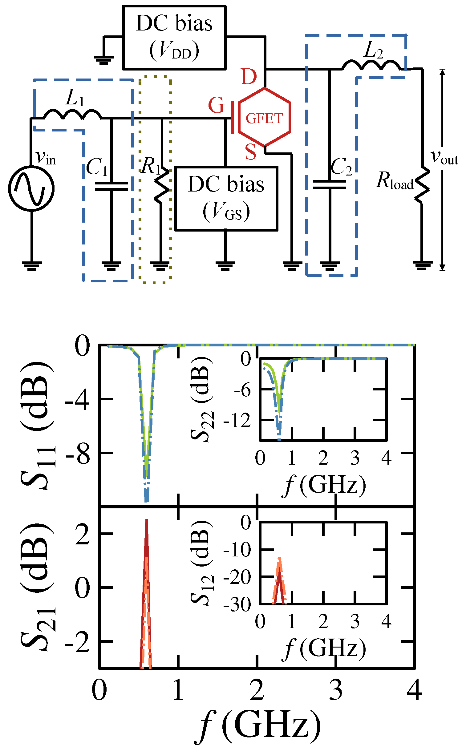
4. Multifunctional Circuit Design and Results

A multifunctional circuit implies using a single device in different circuits with different outcomes: in this case, inverting and in-phase amplification and frequency multiplication ( × 2 ). The first design discussed next is identified as a phase configurable amplifier (PCA). High-frequency amplifiers were designed with the optimized compact model at a frequency of 0.6   G Hz to ensure both current gain (≳5 dB) and unilateral power gain (≳10 dB) within the unipolar bias regions. For the in-phase amplifier, the GFET is biased at V GS 1 = 0.1   V (< V Dirac ) , whereas for the inverting amplifier, V GS 2 = 0.5   V (> V Dirac ) ; in both cases, V DS = 0.3   V . The amplifiers present a low DC power consumption under both bias conditions: ∼40 μ W and ∼200 μ W for the in-phase and inverting amplifiers, respectively. Due to the highly symmetric device transfer characteristics (i.e., similar transconductance and output device resistance at the selected bias points), matching and stability networks for both types of amplifiers have the same topology and elements. The design is shown in the top panel of Figure 3. The DC bias block for the V GS source is suggested to be implemented in a CMOS platform on chip in order to provide the alternative pulses for each circuit function in order to ease a heterogeneous integration of silicon and graphene technologies. Notice that no feedback loop for stability but a padding resistor R 1 was employed toward reducing fabrication processes.
S-parameters for both amplifiers are shown in the bottom panel of Figure 3 considering an input signal of 0.6   G Hz and an input power of −30 dBm. Isolation from ports lower than −10 dB and a power gain of ∼3 dB and ∼1 dB for the in-phase ( @ V GS 1 ) and inverting ( @ V GS 2 ) amplifier designs, respectively, are obtained. The designs are unconditionally stable at the operation frequency regardless of the bias. The input and output signals of the PCA are shown in Figure 4, where the correct outcome of the circuit is observed for both operation modes. The AC voltage gain is 1.3   V / V ( 1.75   V / V ) for the in-phase (inverting amplifier).
The second proposed circuit is a frequency design amplifier (FCA) with the following operation modes: inverting amplification ( @ V GS 2 ) and frequency doubling ( @ V Dirac ), both at V DS = 0.3   V and P in = 30 dBm @ 0.6   GHz . GFET-based FCAs have not been shown elsewhere before. The former operation mode is explained above. For the frequency doubler, the same circuit shown in Figure 3 (the top panel) was used, where all parameter values remain the same with the exception of C 2 , which in this case is 0. The output voltage signal has twice the frequency of v in (cf. the left panel of Figure 5) regardless of the asymmetry of consecutive cycles (associated with a slight asymmetry of the transport due to electrons and holes). The output power P out at 1.2   GHz of the frequency doubler is 45 dBm (cf. Figure 5), yielding a circuit conversion frequency loss of 15 dBm. The power of higher harmonics of the output is below −60 dBm, i.e., ensuring the unique desired response.

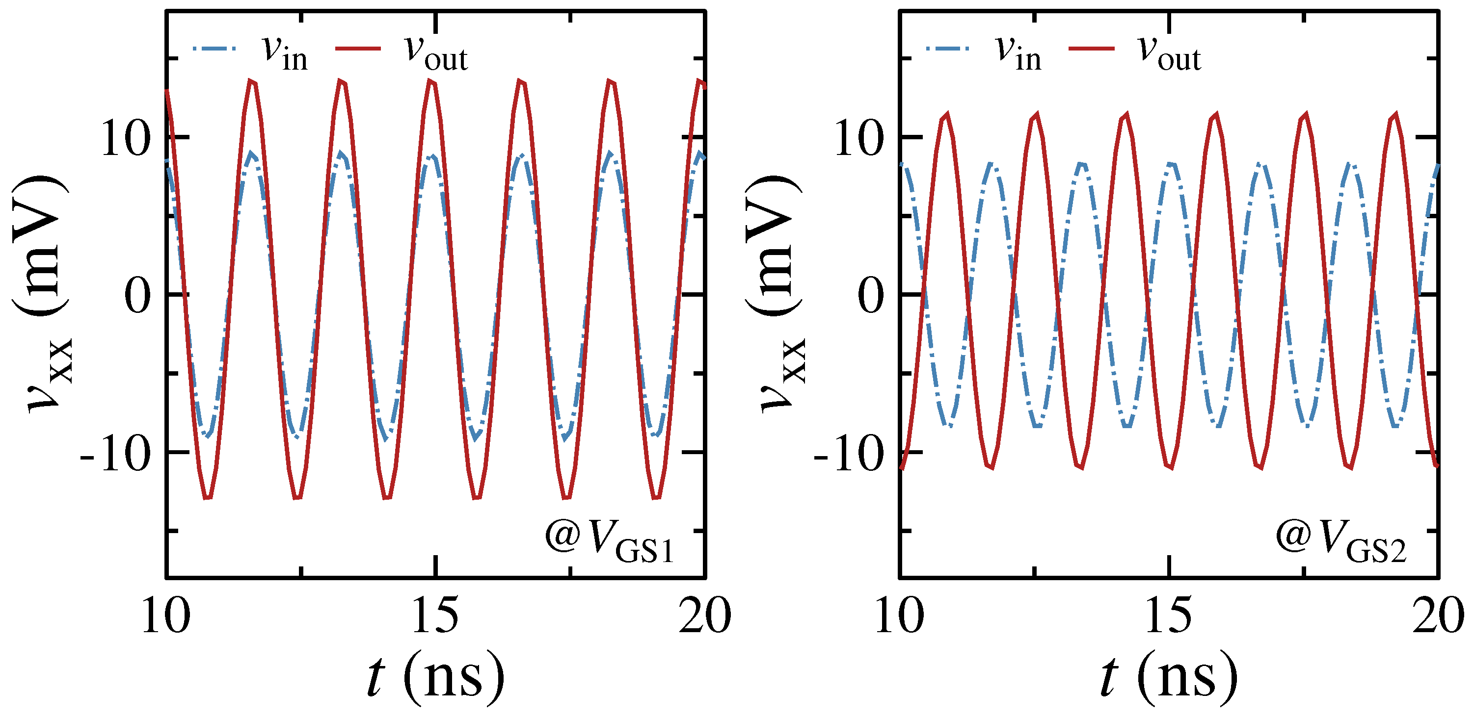
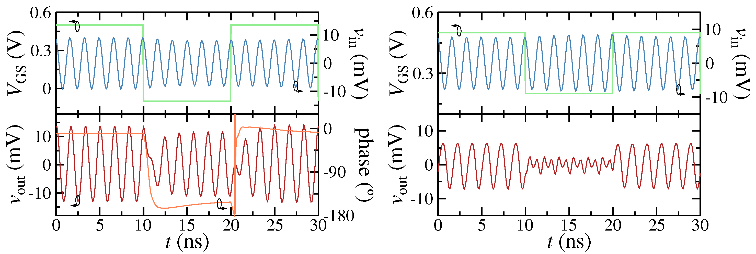
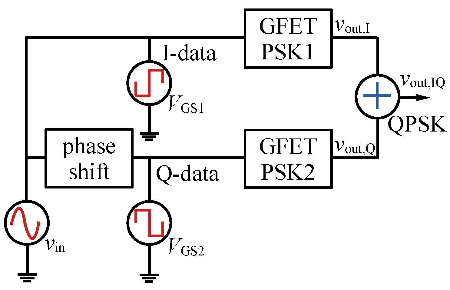
5. Modulator Designs and Results: PSK, FSK and QPSK

By using a pulsed DC bias for V GS with the levels varying between − 0.1   V and 0.5   V , the operation modes of the PCA circuit can be exploited sequentially in order to modify an input AC carrier signal in order to obtain PSK modulation, as shown in the left panel of Figure 6. In addition to the alternating polarity of the DC pulses ensuring similar trap states at each bias point, their 10 n s duration is shorter than the fastest traps reported in the literature for GFET technologies (around hundreds of n s ) [30,31]. The entire PSK circuit can be integrated into a single heterogeneous chip by combining a silicon platform at the FEOL, providing the baseband signal (i.e., V GS pulses) with on-chip pulse generators [32,33], with the GFET-based multifunctional circuit (cf. the top panel of Figure 3) at the BEOL. Furthermore, the circuit architecture of the GFET-based PSK alleviates the use of more than one active device generally found in PSK designs using incumbent technologies [34,35]. The latter implies less production costs and a smaller chip area (if the stability network is properly designed). In contrast to the passive GFET-based modulators found in the literature [10,11,12], this PSK circuit presents an AC gain of ∼ 1.5   V / V and ∼ 1.3   V / V at the ON and OFF state of the baseband pulses, respectively. As a further verification figure of merit, the V GS dependence of the phase of v out is also shown in Figure 6.
In a similar fashion, by combining the operation modes of the FCA, i.e., the inverting amplifier and the frequency doubler, FSK modulation is achieved with one single GFET in the circuit (cf. Figure 3), as shown in the right panel of Figure 7. The frequency of v out at the time frame where the baseband pulse has a value of V GS   =   V Dirac = 0.2   V is twice the value of the signal corresponding to the inverting amplifier operation mode ( V GS = 0.5   V ).
The combination of two identical PSK circuits enables one to obtain a quadrature PSK-modulated signal by applying 90° shifted inputs with identical amplitudes. Hence, a GFET-based QPSK modulator is proposed here by using a pair of the above-discussed PSK circuits, as shown in Figure 7. The input and output signals involved in the QSPK modulation are shown in Figure 8.
The baseband pulsed signals represent different bit streams with a bit duration of 10 n s (a data rate of 0.1 Gbps): V GS 1 represents “10110” whereas V GS 2 corresponds to “11010”. Signals v outI and v outQ are PSK-modulated signals whose change in-phase depends on their corresponding baseband ( V GS 1 and V GS 2 , respectively), as explained above. The combination of the PSK signals yields a phase change of ∼ 45 ° in v outIQ at consecutive bit pairs, as observed in the two bottom panels of Figure 8.

6. Conclusions

Device circuit co-design proposals as the one presented in this work are one of the most efficient approaches to evaluate the impact of emerging transistor technologies in high-performance applications. In this work, a 300 n m long graphene transistor was used as a reference for the calibration of a physics-based compact model and its subsequent optimization toward obtaining a more efficient circuit design. The optimized compact GFET model was used to propose a multifunctional circuit in which one single ambipolar transistor enables bias-dependent outcomes: in-phase amplification if holes dominate the device transport, inverting amplification for the electron-dominated performance and frequency doubling if the device is biased at its charge neutrality point. Hence, a phase configurable amplifier (PCA) is obtained if the GFET is biased alternatively at the p- and n-type regions, whereas by varying V GS between the Dirac voltage and higher values (for an n-type region), a frequency configurable amplifier (FCA) is achieved. By applying a baseband pulsed DC signal along with an AC carrier signal ( 0.6   G Hz ) at the gate of the device, phase-shift keying (PSK) and frequency-shift keying (FSK) modulated output signals can be observed for the PCA and FCA operation modes of the circuit, respectively. GFET-based FSK modulation is proposed for the first time in this work. The combination of two GFET-based PSK modulators yields a quadrature PSK modulation with a data rate of 0.1 Gbps. Regarding the baseband signal, it covers two important aspects of this proposal: (i) it is intended to improve the device reproducibility conditions by diminishing the impact of traps and (ii) it can be implemented with incumbent technologies along with GFETs in a single chip, i.e., enhancing the heterogeneous integration of silicon graphene technologies. From the circuit architecture point of view, this proposal eases the fabrication and chip area of high-data-rate modulators since only one single GFET is used for both PSK and FSK and two GFETs for QPSK, in contrast to the multi-transistor circuits used in incumbent technologies for achieving similar operations.

Author Contributions

Conceptualization, A.P.-S. and J.N.R.-S.; methodology, A.P.-S. and J.N.R.-S.; software, A.P.-S., J.N.R.-S., N.M. and D.J.; validation, A.P.-S., J.N.R.-S. and N.M.; formal analysis, A.P.-S. and J.N.R.-S.; investigation, A.P.-S. and J.N.R.-S.; resources, E.R.-G. and D.J.; data curation, A.P.-S. and J.N.R.-S.; writing—original draft preparation, A.P.-S. and J.N.R.-S.; writing—review and editing, A.P.-S., J.N.R.-S., N.M., E.R.-G. and D.J.; visualization, A.P.-S. and J.N.R.-S.; supervision, A.P.-S.; funding acquisition, A.P.-S., E.R.-G. and D.J. All authors have read and agreed to the published version of the manuscript.

Funding

This work received funding from the European Union’s Horizon 2020 research and innovation program under grant agreement no. GrapheneCore3 881603; from Ministerio de Ciencia, Innovación y Universidades under grant agreements PID2021-127840NB-I00 (MCIN/AEI/FEDER, UE) and FJC2020-046213-I; and from Instituto Politécnico Nacional under the project number SIP/20240622.

Data Availability Statement

The raw data supporting the conclusions of this article will be made available by the authors upon request.

Acknowledgments

The authors would like to acknowledge the DCIS 2023 committee for the invitation to submit this extended paper.

Conflicts of Interest

The authors declare no conflicts of interest.

References

  1. Rudolph, D. Modulation Methods. In Fundamentals of RF and Microwave Techniques and Technologies; Hartnagel, H.L., Quay, R., Rohde, U.L., Rudolph, M., Eds.; Springer: Cham, Switzerland, 2023; pp. 1297–1528. [Google Scholar]
  2. Alimenti, F.; Palazzi, V.; Mariotti, C.; Mezzanotte, P.; Correia, R.; Carvalho, N.B.; Roselli, L. Smart Hardware for Smart Objects: Microwave Electronic Circuits to Make Objects Smart. IEEE Microw. Mag. 2018, 19, 48–68. [Google Scholar] [CrossRef]
  3. Champlain, J.G. On the use of the term “ambipolar”. Appl. Phys. Lett. 2011, 99, 123502. [Google Scholar] [CrossRef]
  4. Moura, R.; Claus, M.; Blawid, S. Multi-mode nanoFETs: From low power to high performance on demand. Semicond. Sci. Technol. 2020, 35, 055027. [Google Scholar] [CrossRef]
  5. Mikolajick, T.; Galderisi, G.; Simon, M.; Rai, S.; Kumar, A.; Heinzig, A.; Weber, W.M.; Trommer, J. 20 Years of reconfigurable field-effect transistors: From concepts to future applications. Solid-State Electron. 2021, 186, 108036. [Google Scholar] [CrossRef]
  6. Das, S.; Das, S. Digital Keying Enabled by Reconfigurable 2D Modulators. Adv. Mater. 2022, 34, 2203753. [Google Scholar] [CrossRef]
  7. Ghivela, G.C.; Sengupta, J. The Promise of Graphene: A Survey of Microwave Devices Based on Graphene. IEEE Microw. Mag. 2020, 21, 48–65. [Google Scholar] [CrossRef]
  8. Hartmann, M.; Hermann, S.; Marsh, P.F.; Rutherglen, C.; Wang, D.; Ding, L.; Peng, L.-M.; Claus, M.; Schröter, M. CNTFET technology for RF applications: Review and future perspective. IEEE J. Microw. 2021, 1, 275–287. [Google Scholar] [CrossRef]
  9. Ramos-Silva, J.N.; Pacheco-Sanchez, A.; Ramirez-Garcia, E.; Jiménez, D. Multifunctional high-frequency circuit capabilities of ambipolar carbon nanotube FETs. IEEE Trans. Nanotechnol. 2021, 20, 474–480. [Google Scholar] [CrossRef]
  10. Yang, X.; Liu, G.; Balandin, A.A.; Mohanram, K. Triple-Mode Single-Transistor Graphene Amplifier and Its Applications. ACS Nano 2010, 4, 5532–5538. [Google Scholar] [CrossRef]
  11. Lee, S.; Lee, K.; Liu, C.-H.; Kulkarni, G.S.; Zhong, Z. Flexible and transparent all-graphene circuits for quaternary digital modulations. Nat. Commun. 2012, 3, 1018. [Google Scholar] [CrossRef]
  12. Habibpour, O.; He, Z.S.; Strupinski, W.; Rorsman, N.; Ciuk, T.; Ciepielewski, P.; Zirath, H. Graphene FET Gigabit ON–OFF Keying Demodulator at 96 GHz. IEEE Electron. Device Lett. 2016, 37, 333–336. [Google Scholar] [CrossRef]
  13. Habibpour, O.; He, Z.S.; Strupinski, W.; Rorsman, N.; Zirath, H. Wafer scale millimeter-wave integrated circuits based on epitaxial graphene in high data rate communication. Sci. Rep. 2017, 7, 41828. [Google Scholar] [CrossRef]
  14. Saeed, M.; Palacios, P.; Wei, M.-D.; Baskent, E.; Fan, C.-Y.; Uzlu, B.; Wang, K.-T.; Hemmetter, A.; Wang, Z.; Neumaier, D.; et al. Graphene-Based Microwave Circuits: A Review. Adv. Mater. 2022, 34, 2108473. [Google Scholar] [CrossRef]
  15. Tateno, Y.; Mitsuhashi, F.; Adachi, M.; Yonemura, T.; Saito, Y.; Yamamoto, Y.; Nakabayashi, T. An investigation to determine the interface condition between graphene and aluminum oxide. Jpn. J. Appl. Phys. 2020, 59, 124001. [Google Scholar] [CrossRef]
  16. Pacheco-Sanchez, A.; Mavredakis, N.; Feijoo, P.C.; Wei, W.; Pallecchi, E.; Happy, H.; Jiménez, D. Experimental observation and modeling of the impact of traps on static and analog/HF performance of graphene transistors. IEEE Trans. Electron Devices 2020, 67, 5790–5796. [Google Scholar] [CrossRef]
  17. Knobloch, T.; Uzlu, B.; Illarionov, Y.; Wang, Z.; Otto, M.; Filipovic, L.; Waltl, M.; Neumaier, D.; Lemme, M.C.; Grasser, T. Improving stability in two-dimensional transistors with amorphous gate oxides by Fermi-level tuning. Nat. Electron. 2022, 5, 356–366. [Google Scholar] [CrossRef]
  18. Ribes, G.; Mitard, J.; Denais, M.; Bruyere, S.; Monsieur, F.; Parthasarathy, C.; Vincent, E.; Ghibaudo, G. Review on high-k dielectrics reliability issues. IEEE Trans. Device Mater. Reliab. 2005, 5, 5–19. [Google Scholar] [CrossRef]
  19. Hong, S.K.; Kim, C.S.; Hwang, W.S.; Cho, B.J. Hybrid Integration of Graphene Analog and Silicon Complementary Metal-Oxide-Semiconductor Digital Circuits. ACS Nano 2016, 10, 7142–7146. [Google Scholar] [CrossRef]
  20. Akinwande, D.; Huyghebaert, C.; Wang, C.-H.; Serna, M.I.; Goossens, S.; Li, L.-J.; Philip Wong, H.-S.; Koppens, F.H.L. Graphene and twodimensional materials for silicon technology. Nature 2019, 573, 507–518. [Google Scholar] [CrossRef]
  21. Pacheco-Sanchez, A.; Ramos-Silva, J.N.; Mavredakis, N.; Ramírez-García, E.; Jiménez, D. Design of GFET-based active modulators leveraging device performance reproducibility conditions. In Proceedings of the IEEE Conference on Design of Circuits and Integrated Systems (DCIS), Malaga, Spain, 15–17 November 2023. [Google Scholar]
  22. Pasadas, F.; Medina-Rull, A.; Ruiz, F.G.; Ramos-Silva, J.N.; Pacheco-Sanchez, A.; Pardo, M.C.; Toral-Lopez, A.; Godoy, A.; Ramírez-García, E.; Jiménez, D.; et al. Exploiting ambipolarity in graphene field-effect transistors for novel designs on high-frequency analog electronics. Small 2023, 19, 2303595. [Google Scholar] [CrossRef]
  23. Heinzig, A.; Slesazeck, S.; Kreupl, F.; Mikolajick, T.; Weber, W.M. Reconfigurable Silicon Nanowire Transistors. Nano Lett. 2012, 12, 119–124. [Google Scholar] [CrossRef] [PubMed]
  24. Pasadas, F.; Feijoo, P.C.; Mavredakis, N.; Pacheco-Sanchez, A.; Chaves, F.A.; Jiménez, D. Compact modeling technology for the simulation of integrated circuits based on graphene field-effect transistors. Adv. Mater. 2022, 34, 2201691. [Google Scholar] [CrossRef]
  25. Mavredakis, N.; Pacheco-Sanchez, A.; Txoperena, O.; Torres, E.; Jiménez, D. A Scalable Compact Model for the Static Drain Current of Graphene FETs. IEEE Trans. Electron Devices 2024, 71, 853–859. [Google Scholar] [CrossRef]
  26. Wei, W.; Zhou, X.; Deokar, G.; Kim, H.; Belhaj, M.M.; Galopin, E.; Pallecchi, E.; Happy, H. Graphene FETs with aluminum bottom-gate electrodes and its natural oxide as dielectrics. IEEE Trans. ONE Devices 2015, 62, 2769–2773. [Google Scholar] [CrossRef]
  27. Toral-Lopez, A.; Marin, E.G.; Pasadas, F.; Gonzalez-Medina, J.M.; Ruiz, F.G.; Jiménez, D.; Godoy, A. GFET Asymmetric Transfer Response Analysis through Access Region Resistances. Nanomaterials 2019, 9, 1027. [Google Scholar] [CrossRef]
  28. Zhang, Z.; Xu, H.; Zhong, H.; Peng, L.-M. Direct extraction of carrier mobility in graphene field-effect transistor using current-voltage and capacitance-voltage measurements. Appl. Phys. Lett. 2012, 101, 213101. [Google Scholar] [CrossRef]
  29. Gahoi, A.; Kataria, S.; Driussi, F.; Venica, S.; Pandey, H.; Esseni, D.; Selmi, L.; Lemme, M.C. Dependable Contact Related Parameter Extraction in Graphene–Metal Junctions. Adv. Electron. Mater. 2020, 6, 2000386. [Google Scholar] [CrossRef]
  30. Carrion, E.A.; Serov, A.Y.; Islam, S.; Behnam, A.; Malik, A.; Xiong, F.; Bianchi, M.; Sordan, R.; Pop, E. Hysteresis-Free Nanosecond Pulsed Electrical Characterization of Top-Gated Graphene Transistors. IEEE Trans. Electron Devices 2014, 61, 1583–1589. [Google Scholar] [CrossRef]
  31. Nathawat, J.; Zhao, M.; Kwan, C.-P.; Yin, S.; Arabchigavkani, N.; Randle, M.; Ramamoorthy, H.; He, G.; Somphonsane, R.; Matsumoto, N.; et al. Transient Response of h-BN-Encapsulated Graphene Transistors: Signatures of Self-Heating and Hot-Carrier Trapping. ACS Omega 2019, 4, 4082–4090. [Google Scholar] [CrossRef]
  32. Zhu, Y.; Zuegel, J.D.; Marciante, J.R.; Wu, H. Distributed Waveform Generator: A New Circuit Technique for Ultra-Wideband Pulse Generation, Shaping and Modulation. IEEE J. Solid-State Circuits 2009, 44, 808–823. [Google Scholar] [CrossRef]
  33. Sneler, L.; Matic, T.; Herceg, M. A Tunable CMOS IR-UWB Pulse Generator Based on Feedback Controlled Oscillator Switching. IEEE Trans. Circuits Syst. II Express Briefs 2021, 68, 1902–1906. [Google Scholar] [CrossRef]
  34. Karthaus, U.; Fischer, M. Fully integrated passive UHF RFID transponder IC with 16.7-uW minimum RF input power. IEEE J. Solid-State Circuits 2003, 38, 1602–1608. [Google Scholar] [CrossRef]
  35. Carlowitz, C.; Vossiek, M. PSK Modulator for Regenerative Sampling Gigabit UWB Communication. In Proceedings of the GeMiC 2014; German Microwave Conference, Aachen, Germany, 10–12 March 2014. [Google Scholar]
Figure 1. Top left: ambipolar transfer characteristic of a GFET showing approximate definitions for the drain current in the different operation regimes. Bottom left: input AC signals. Top right: output AC signal. Bottom right: equations of the analog AC+DC signals for the general case (in black) and specific cases. A, B, C, D and E are arbitrary constants and Γ = 0.5 R d C A 2 , Φ = V DS B R d and R d is the output resistance seen from the drain terminal. I d is obtained by replacing V GS with V GS + v in in the corresponding I D .
Electronics 13 04022 g001
Figure 2. Transfer characteristics of a 300 n m long GFET. Left: Trap-reduced data obtained with opposing pulses. Markers are experimental data and lines are modeling results. Inset shows the applied opposing V GS pulses and constant V DS . Right panel: optimized device modeling results. V DS is 0.1 V, 0.2 V and 0.3 V for all cases.
Electronics 13 04022 g002
Figure 3. Top: Schematic of the multifunctional GFET circuit used for data modulation at 0.6   GHz . In-phase and inverting amplification obtained with V GS equal to −0.1 V and 0.5 V , respectively, whereas the circuit works as a frequency doubler at V GS = V Dirac . Matching (stability) networks are indicated by the dashed (dotted) boxes and are the same regardless of the operation mode. DC and AC filtering between signal sources and circuit elements are not shown. Input AC power is of 30 dBm at 0.6   GHz . Values of circuit elements are L 1 = 155   n H , C 1 = 375   f F , L 2 = 41   n H , C 2 = 1.6   p F , R 1 = 10.9   k Ω . V DD = 0.3   V . Bottom: S-parameters of the amplifiers for the PCA design: continuous lines represent results of the in-phase amplifier ( @ V GS 1 ) and dashed–dotted lines show results of the inverting amplifier ( @ V GS 2 ).
Electronics 13 04022 g003
Figure 4. v in and v out signals for the PCA design in both operation modes: In-phase amplifier (left) and inverting amplifier (right). Only a 10 n s fram is shown for a better visualization of the signals.
Electronics 13 04022 g004
Figure 5. Frequency doubler results: v in and v out signals over a 10 n s frame (left) and output power spectrum over frequency (right).
Electronics 13 04022 g005
Figure 6. Baseband, carrier and modulated signals achieved with the GFET-based multifunctional circuits. Left: PSK signals. Phase of output signal is included in the bottom plot. Right: FSK signals.
Electronics 13 04022 g006
Figure 7. Schematic representation of 0.6   M Hz -QPSK modulator obtained with two GFET-based PSK circuits. Each PSK block corresponds to the circuit shown in Figure 3. V GS 1 and V GS 2 correspond to the baseband signal of the PCA design (with values of − 0.1 V and 0.5 V ).
Electronics 13 04022 g007
Figure 8. Signals involved in the GFET-based quadrature PSK modulation.
Electronics 13 04022 g008
Disclaimer/Publisher’s Note: The statements, opinions and data contained in all publications are solely those of the individual author(s) and contributor(s) and not of MDPI and/or the editor(s). MDPI and/or the editor(s) disclaim responsibility for any injury to people or property resulting from any ideas, methods, instructions or products referred to in the content.

