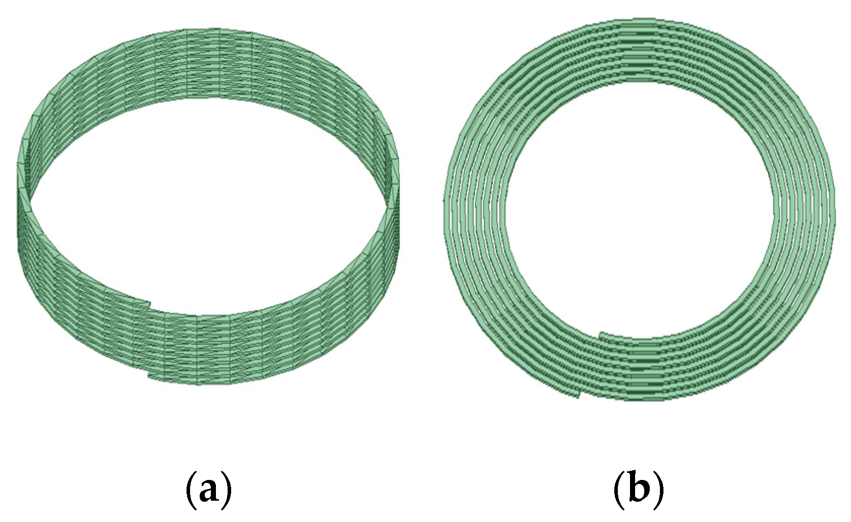
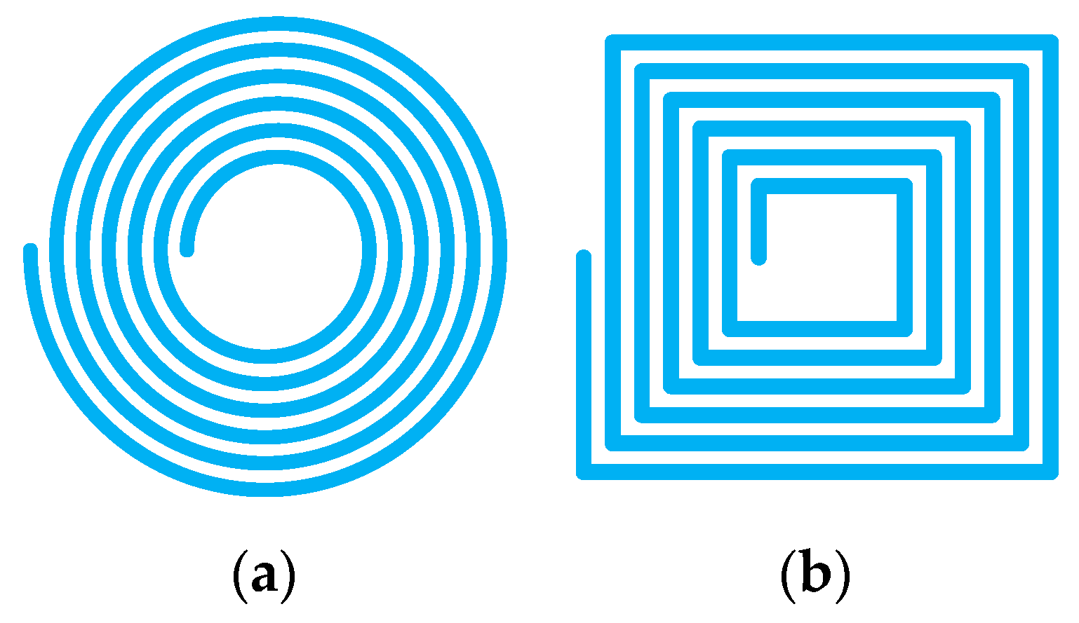
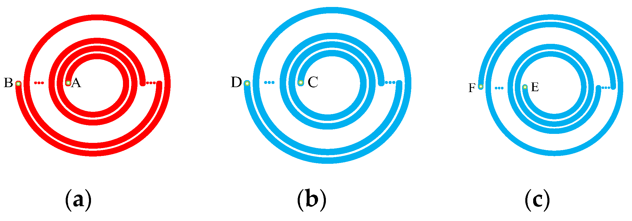
Figure 1.
Two types of coil structures: (a) spatial spiral structure, (b) planar spiral structure.
Figure 1.
Two types of coil structures: (a) spatial spiral structure, (b) planar spiral structure.
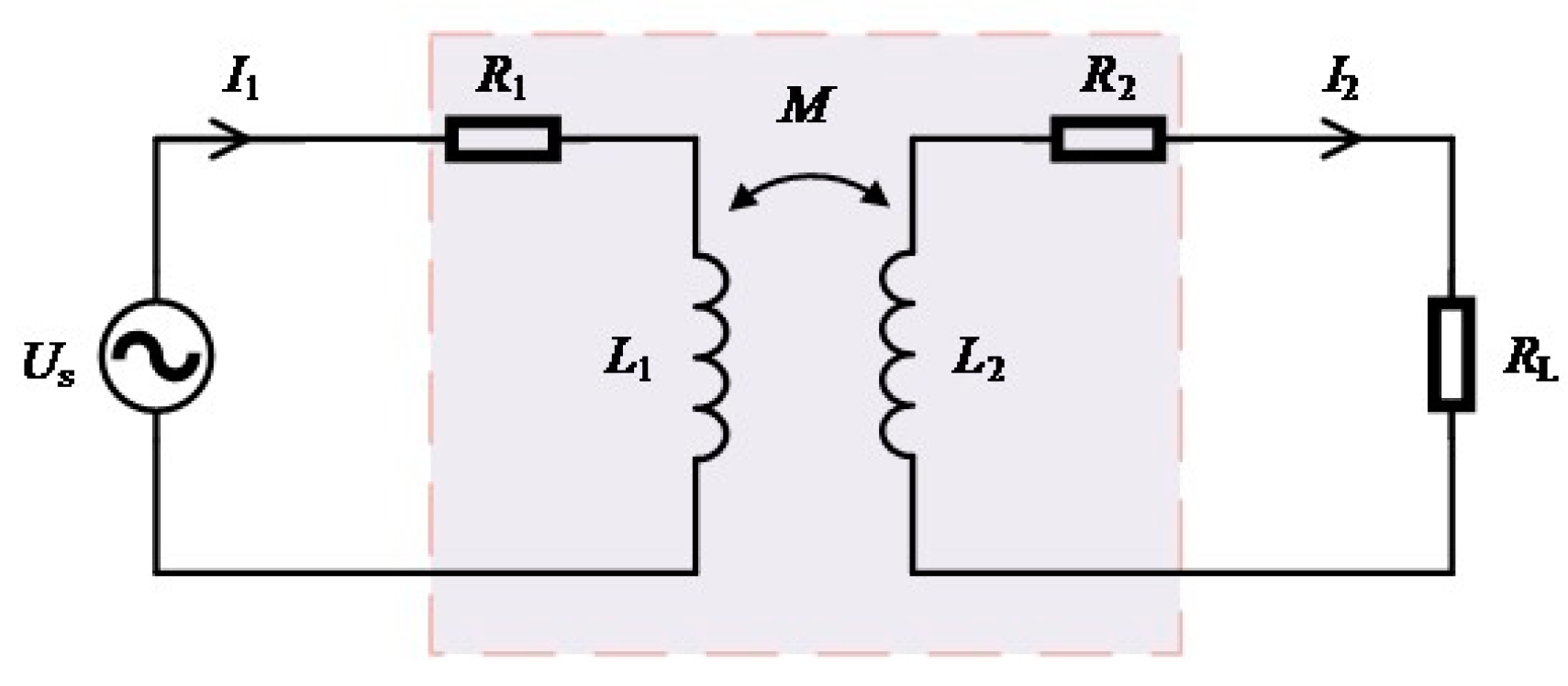
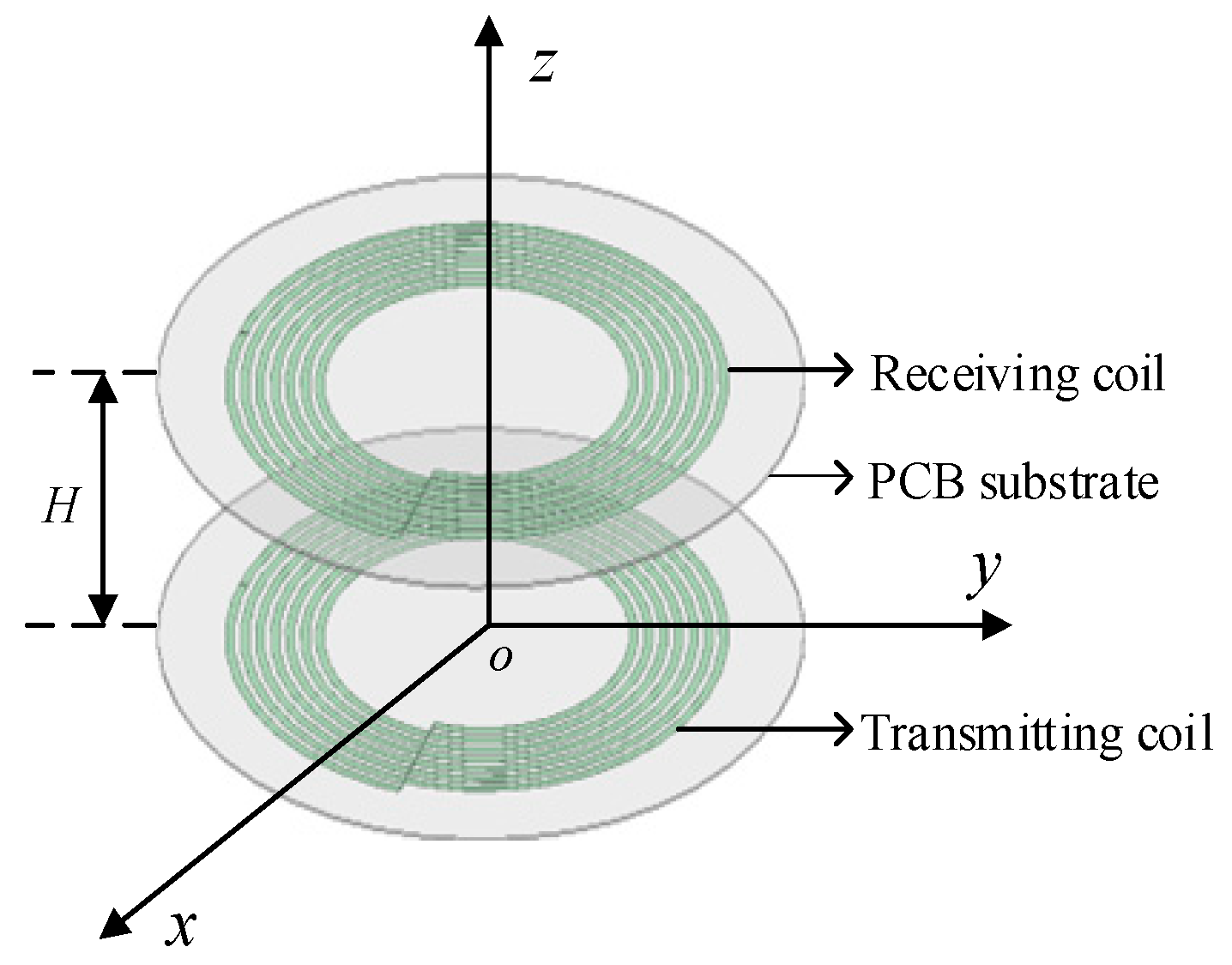
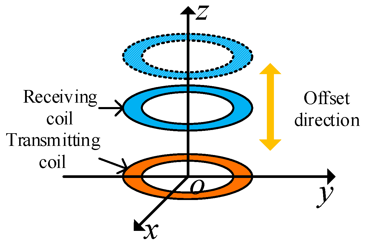
Figure 2.
Structure diagram of the wireless power transfer system.
Figure 2.
Structure diagram of the wireless power transfer system.
Figure 3.
Coupled coil mutual inductance circuit model.
Figure 3.
Coupled coil mutual inductance circuit model.
Figure 4.
Circuit figure of the bilateral compensation method: (a) SS-type compensation; (b) SP-type compensation; (c) PS-type compensation; (d) PP-type compensation.
Figure 4.
Circuit figure of the bilateral compensation method: (a) SS-type compensation; (b) SP-type compensation; (c) PS-type compensation; (d) PP-type compensation.
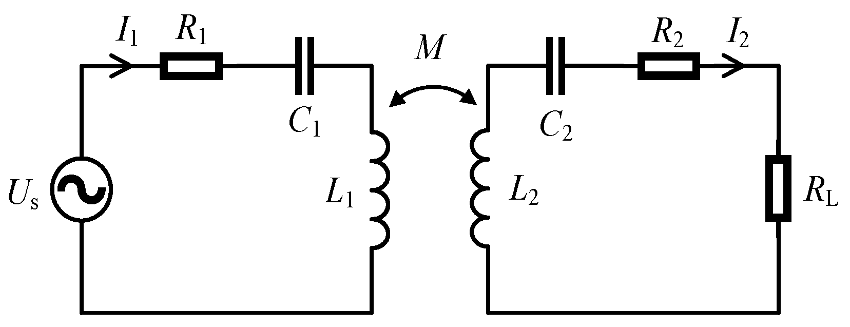
Figure 5.
Coupling coil mutual inductance circuit model of the SS compensation method.
Figure 5.
Coupling coil mutual inductance circuit model of the SS compensation method.
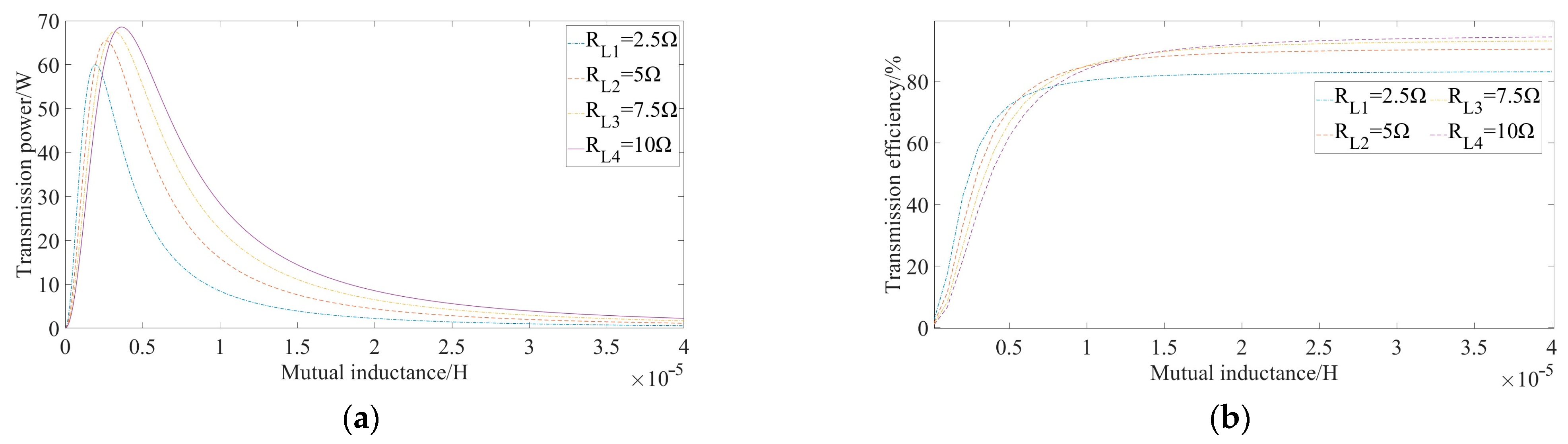
Figure 6.
Relationship between coil mutual inductance and transmission power and efficiency under different load resistances: (a) coil transmission power; (b) coil transmission efficiency.
Figure 6.
Relationship between coil mutual inductance and transmission power and efficiency under different load resistances: (a) coil transmission power; (b) coil transmission efficiency.
Figure 7.
Flat coils with different shapes: (a) circular plane spiral coil; (b) square plane spiral coil.
Figure 7.
Flat coils with different shapes: (a) circular plane spiral coil; (b) square plane spiral coil.
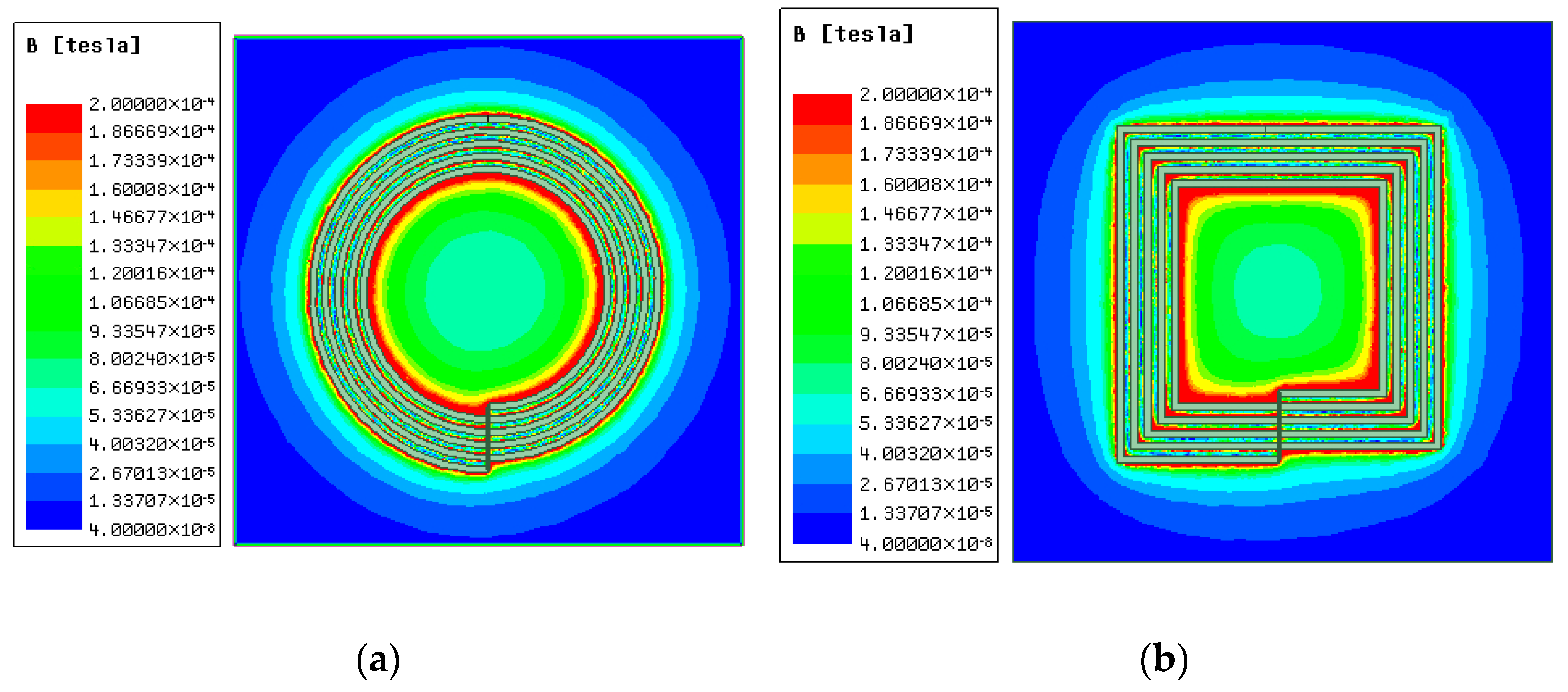
Figure 8.
Magnetic field nephogram of plane coils with different shapes: (a) circular plane spiral coil; (b) square plane spiral coil.
Figure 8.
Magnetic field nephogram of plane coils with different shapes: (a) circular plane spiral coil; (b) square plane spiral coil.
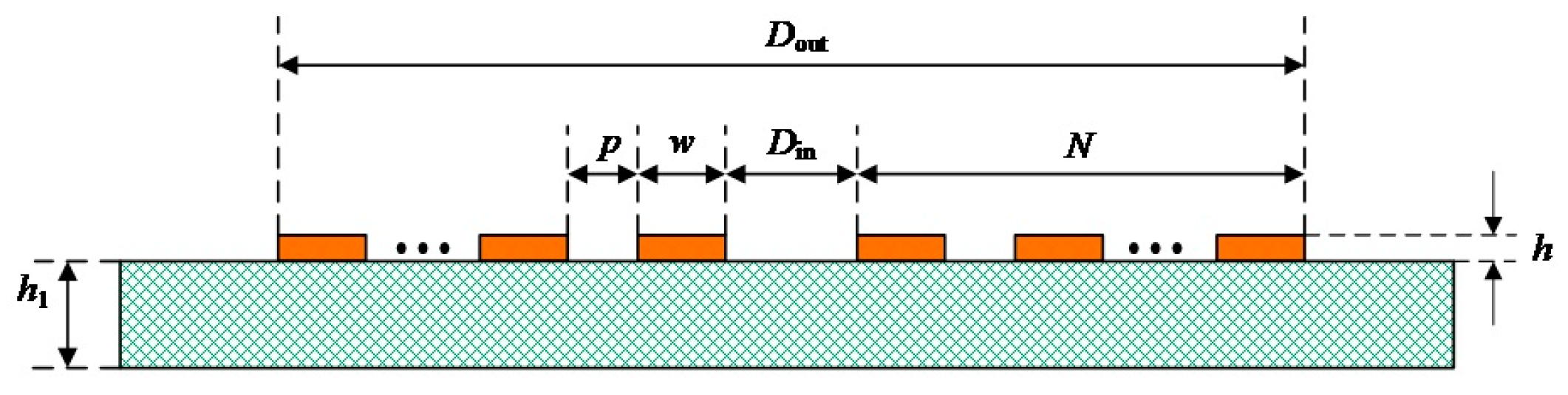
Figure 9.
Sectional figure of the PCB plane circular coil.
Figure 9.
Sectional figure of the PCB plane circular coil.
Figure 10.
Three-dimensional simulation model of the coil.
Figure 10.
Three-dimensional simulation model of the coil.
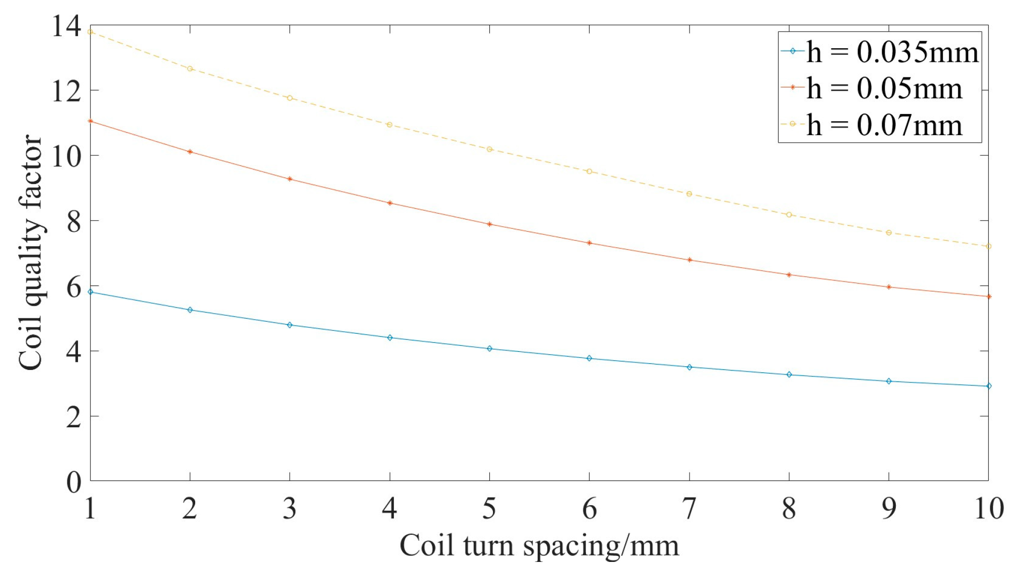
Figure 11.
Quality factor with different thicknesses.
Figure 11.
Quality factor with different thicknesses.
Figure 12.
Simulation results of different coil turn spacings: (a) coil quality factor and coupling coefficient; (b) strong coupling coefficient of coil.
Figure 12.
Simulation results of different coil turn spacings: (a) coil quality factor and coupling coefficient; (b) strong coupling coefficient of coil.
Figure 13.
Simulation results of different coilline width: (a) coil quality factor and coupling coefficient; (b) strong coupling coefficient of coil.
Figure 13.
Simulation results of different coilline width: (a) coil quality factor and coupling coefficient; (b) strong coupling coefficient of coil.
Figure 14.
Simulation data of different coil turns: (a) coil quality factor and coupling coefficient; (b) strong coupling coefficient of coil.
Figure 14.
Simulation data of different coil turns: (a) coil quality factor and coupling coefficient; (b) strong coupling coefficient of coil.
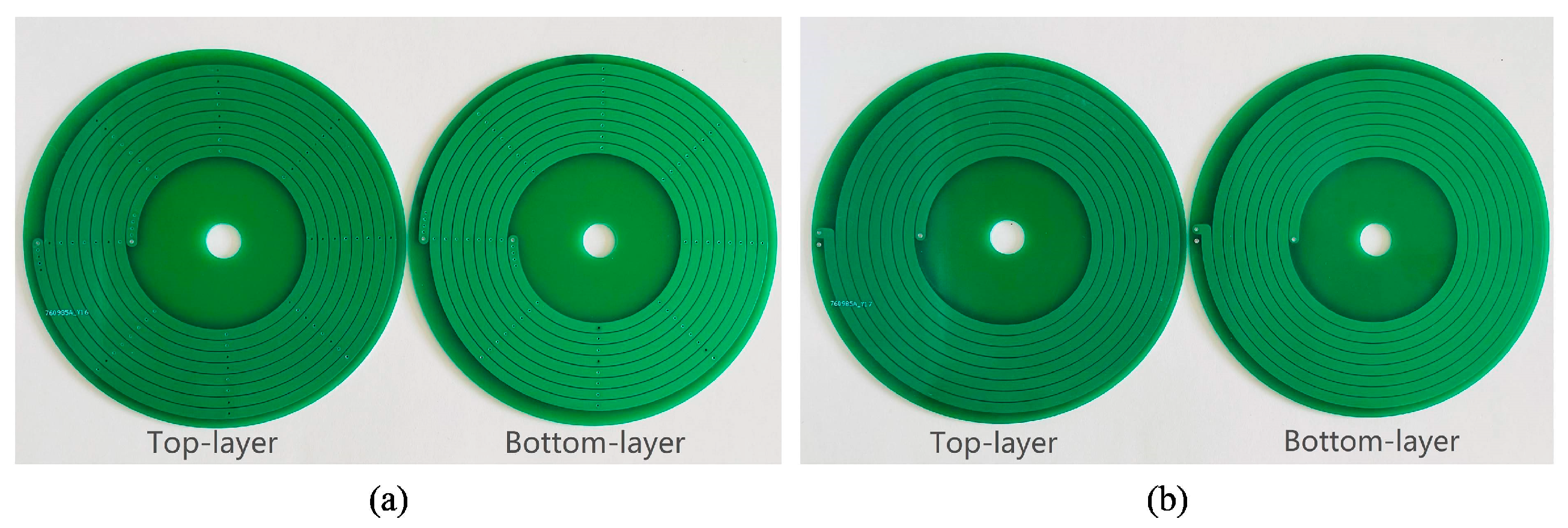
Figure 15.
Top view of the double-layer PCB coil: (a) top view of the coil top layer; (b) top view of the coil bottom layer in Scheme 1; (c) top view of the coil bottom layer in Scheme 2.
Figure 15.
Top view of the double-layer PCB coil: (a) top view of the coil top layer; (b) top view of the coil bottom layer in Scheme 1; (c) top view of the coil bottom layer in Scheme 2.
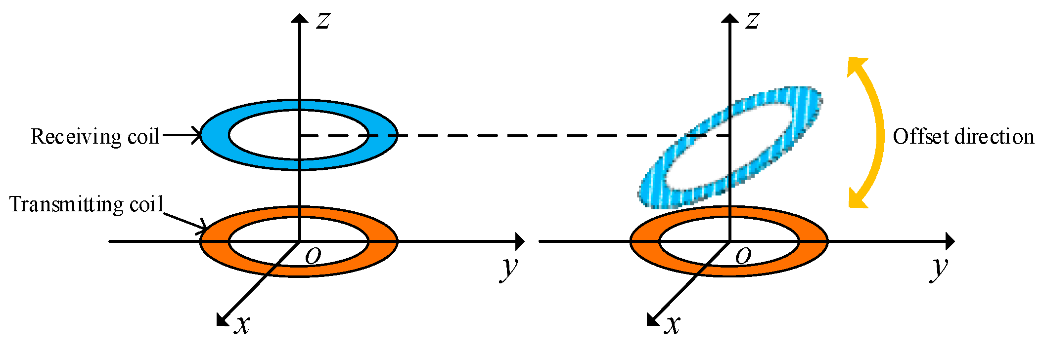
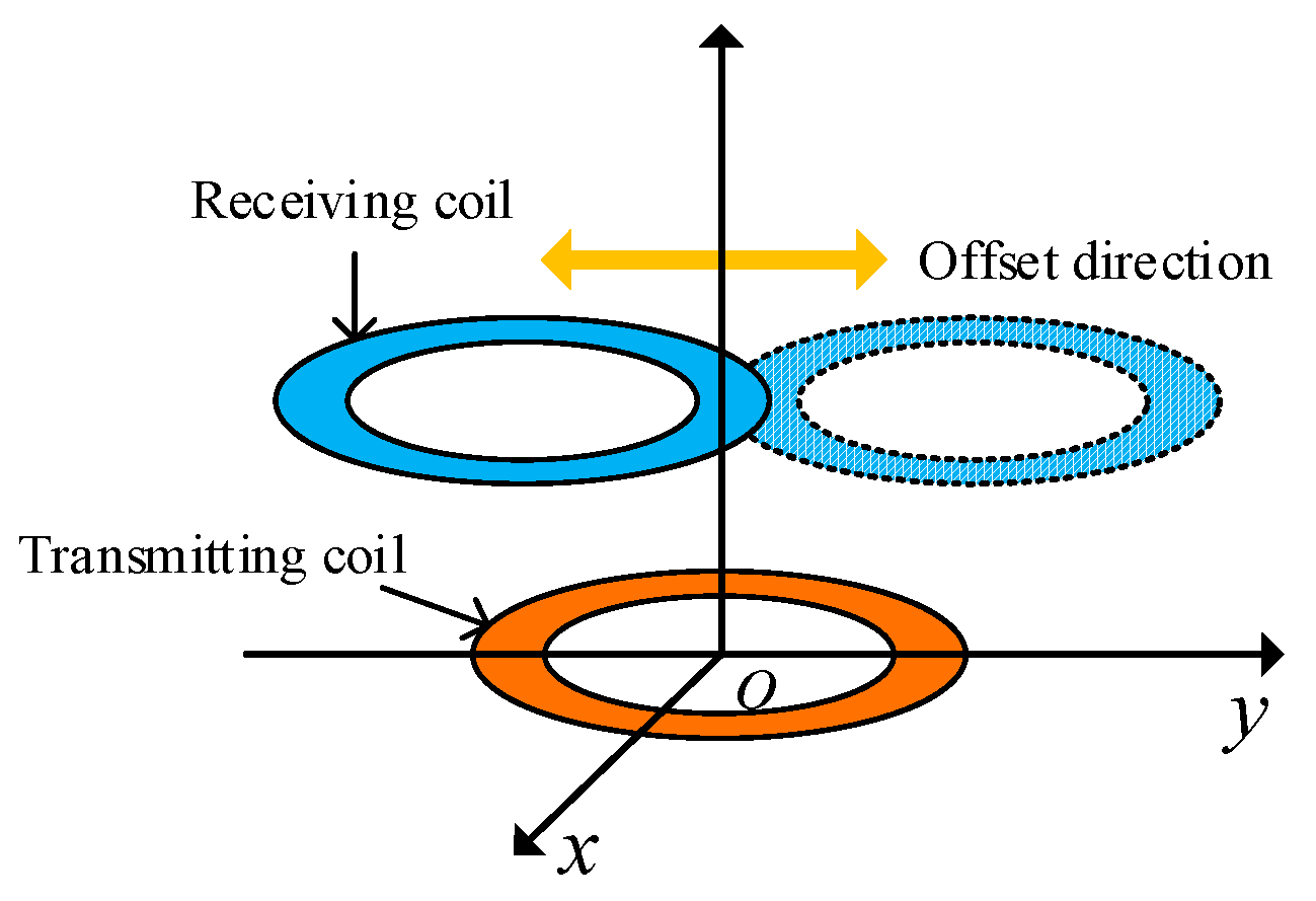
Figure 16.
Model figure of coil coaxial parallel offset.
Figure 16.
Model figure of coil coaxial parallel offset.
Figure 17.
Schematic figure of coil coaxial parallel offset: (a) offset 3 cm; (b) offset 5 cm; (c) offset 7 cm.
Figure 17.
Schematic figure of coil coaxial parallel offset: (a) offset 3 cm; (b) offset 5 cm; (c) offset 7 cm.
Figure 18.
Simulation data of coil coaxial parallel offset: (a) coil coupling coefficient; (b) coil strong coupling coefficient; (c) coil transmission efficiency.
Figure 18.
Simulation data of coil coaxial parallel offset: (a) coil coupling coefficient; (b) coil strong coupling coefficient; (c) coil transmission efficiency.
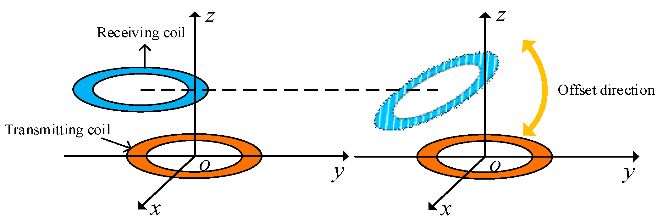
Figure 19.
Schematic figure of coil coaxial nonparallel offset.
Figure 19.
Schematic figure of coil coaxial nonparallel offset.
Figure 20.
Model figure of coil coaxial nonparallel offset: (a) offset 5 cm, offset 30 degrees; (b) offset 5 cm, offset 60 degrees; (c) offset 7 cm, offset 30 degrees.
Figure 20.
Model figure of coil coaxial nonparallel offset: (a) offset 5 cm, offset 30 degrees; (b) offset 5 cm, offset 60 degrees; (c) offset 7 cm, offset 30 degrees.
Figure 21.
Simulation results of coil coaxial nonparallel offset: (a) coil coupling coefficient; (b) coil strong coupling coefficient; (c) coil transmission efficiency; (d) comparison of strong coupling coefficients at different offset angles under the condition of an offset distance of 5.5 cm.
Figure 21.
Simulation results of coil coaxial nonparallel offset: (a) coil coupling coefficient; (b) coil strong coupling coefficient; (c) coil transmission efficiency; (d) comparison of strong coupling coefficients at different offset angles under the condition of an offset distance of 5.5 cm.
Figure 22.
Schematic figure of coil different axes parallel offset.
Figure 22.
Schematic figure of coil different axes parallel offset.
Figure 23.
Model figure of different axes used for the parallel offset of coil: (a) offset 1 cm; (b) offset 2.5 cm; (c) offset 4 cm.
Figure 23.
Model figure of different axes used for the parallel offset of coil: (a) offset 1 cm; (b) offset 2.5 cm; (c) offset 4 cm.
Figure 24.
Simulation data of coils with different parallel offset axes: (a) coil coupling coefficient; (b) coil strong coupling coefficient; (c) coil transmission efficiency.
Figure 24.
Simulation data of coils with different parallel offset axes: (a) coil coupling coefficient; (b) coil strong coupling coefficient; (c) coil transmission efficiency.
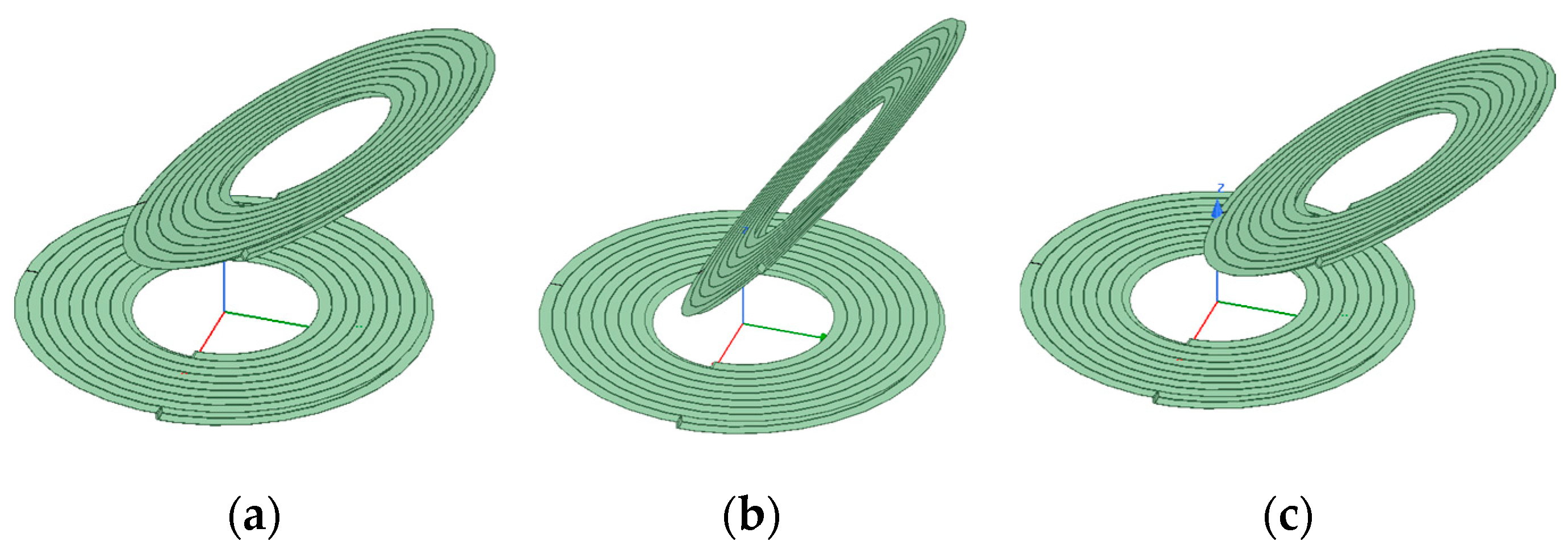
Figure 25.
Schematic figure of different axes of nonparallel offset of coils.
Figure 25.
Schematic figure of different axes of nonparallel offset of coils.
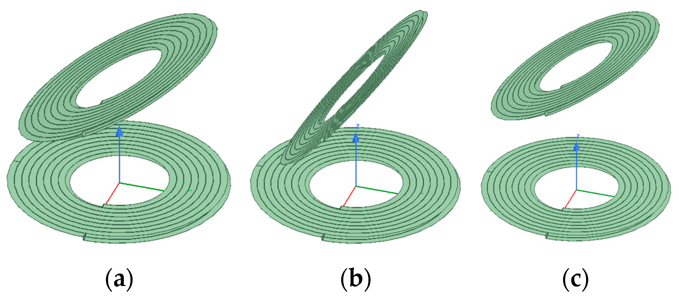
Figure 26.
Model figure of coil different axes nonparallel offset: (a) offset 2 cm, angle 30 degrees; (b) offset 2 cm, angle 60 degrees; (c) offset 4 cm, angle 30 degrees.
Figure 26.
Model figure of coil different axes nonparallel offset: (a) offset 2 cm, angle 30 degrees; (b) offset 2 cm, angle 60 degrees; (c) offset 4 cm, angle 30 degrees.
Figure 27.
Simulation data of coils with different nonparallel offset axes: (a) coil coupling coefficient; (b) coil strong coupling coefficient; (c) coil transmission efficiency; (d) comparison of strong coupling coefficients at different offset angles under the condition of a 1 cm offset distance.
Figure 27.
Simulation data of coils with different nonparallel offset axes: (a) coil coupling coefficient; (b) coil strong coupling coefficient; (c) coil transmission efficiency; (d) comparison of strong coupling coefficients at different offset angles under the condition of a 1 cm offset distance.
Figure 28.
Physical figure of a single-layer coil: (a) coil 1; (b) coil 2; (c) coil 3; (d) coil 4; (e) coil 5; (f) coil 6; (g) coil 7; (h) coil 8; (i) coil 9.
Figure 28.
Physical figure of a single-layer coil: (a) coil 1; (b) coil 2; (c) coil 3; (d) coil 4; (e) coil 5; (f) coil 6; (g) coil 7; (h) coil 8; (i) coil 9.
Figure 29.
Physical figure of a double-layer coil: (a) coil 10; (b) coil 11.
Figure 29.
Physical figure of a double-layer coil: (a) coil 10; (b) coil 11.
Figure 30.
Experimental platform for coil parameter measurement: (a) self-inductance measurement; (b) mutual inductance measurement.
Figure 30.
Experimental platform for coil parameter measurement: (a) self-inductance measurement; (b) mutual inductance measurement.
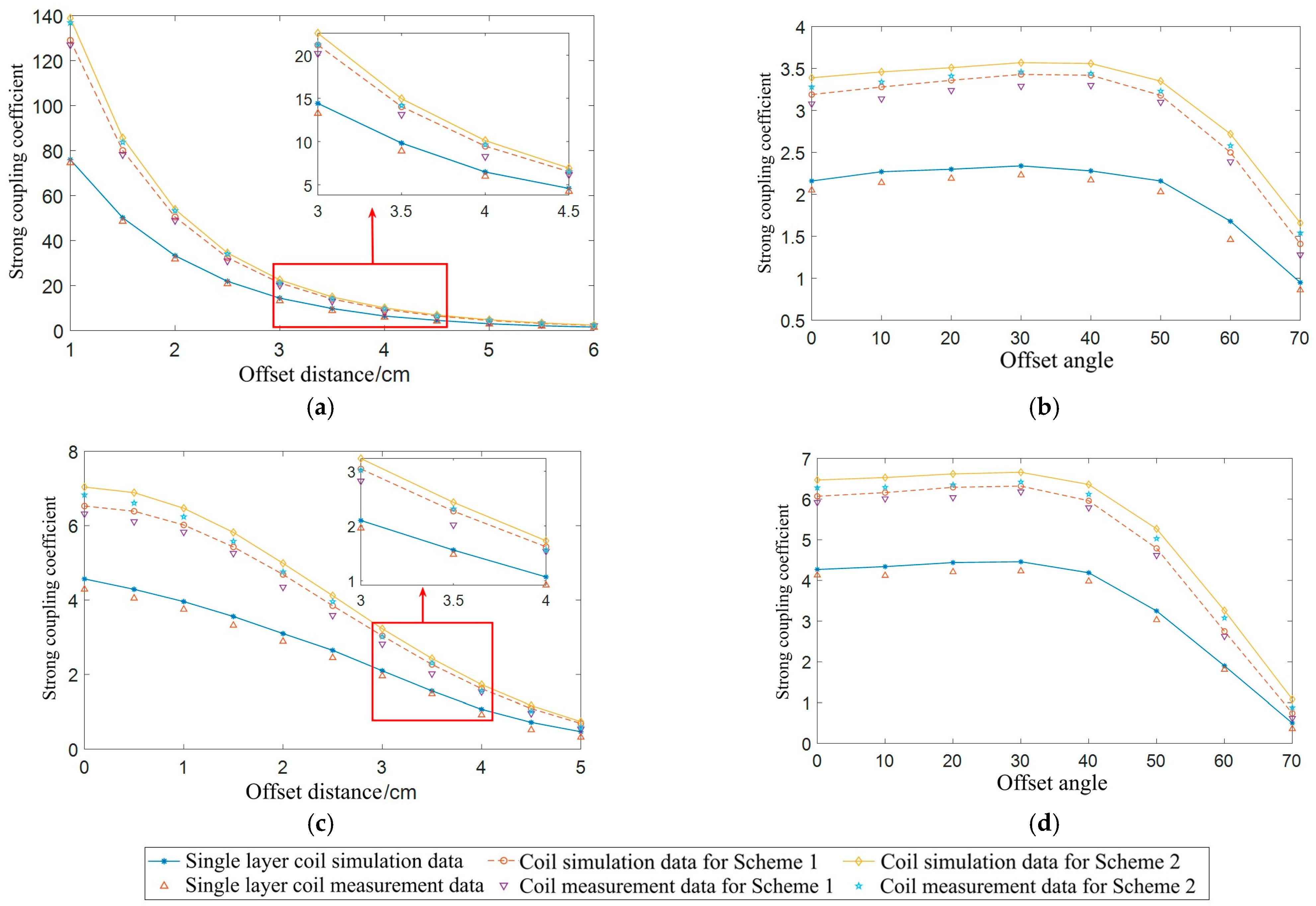
Figure 31.
Simulation data and measurement calculation data of the strong coupling coefficient for coil offset: (a) coaxial parallel offset; (b) coaxial nonparallel offset; (c) parallel offset of different axes; (d) different axes are not parallel offset.
Figure 31.
Simulation data and measurement calculation data of the strong coupling coefficient for coil offset: (a) coaxial parallel offset; (b) coaxial nonparallel offset; (c) parallel offset of different axes; (d) different axes are not parallel offset.
Figure 32.
Wireless power transfer system experimental platform.
Figure 32.
Wireless power transfer system experimental platform.
Figure 33.
Oscilloscope-measured waveform: (a) voltage (red) and current (blue) waveforms at the transmitting end; (b) load voltage (red) and current (blue) waveform at the receiving end.
Figure 33.
Oscilloscope-measured waveform: (a) voltage (red) and current (blue) waveforms at the transmitting end; (b) load voltage (red) and current (blue) waveform at the receiving end.
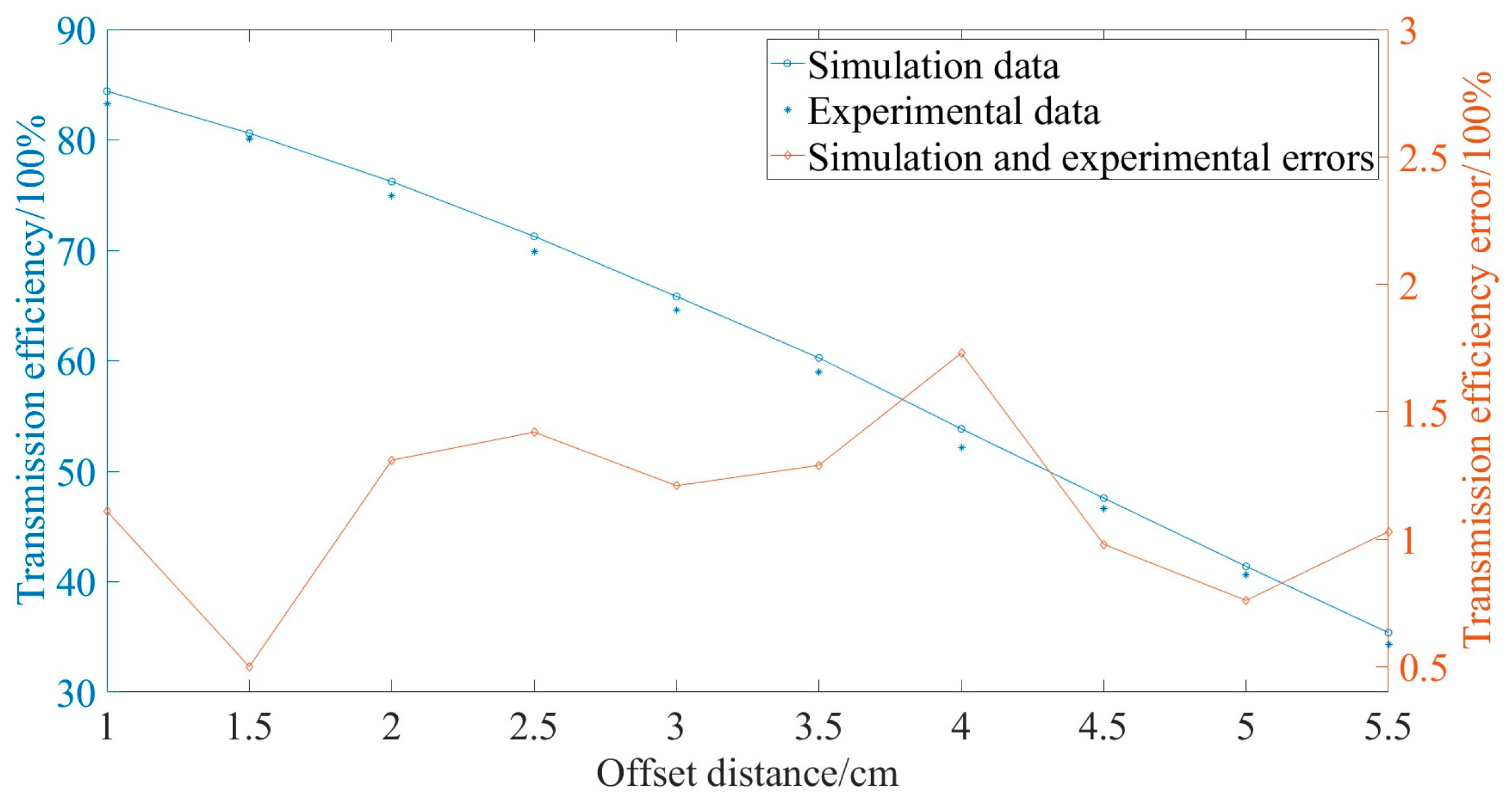
Figure 34.
Simulation and experimental data on coil transmission efficiency.
Figure 34.
Simulation and experimental data on coil transmission efficiency.
Table 1.
Reflecting resistance and reflecting reactance at the receiving end.
Table 1.
Reflecting resistance and reflecting reactance at the receiving end.
Receiving Capacitance
Compensation Method | Capacitor in Series | Capacitor in Parallel |
|---|
| Reflective resistance Rr | | |
| Reflective reactance X | 0 | |
Table 2.
Different compensation methods for the capacitor value.
Table 2.
Different compensation methods for the capacitor value.
| Compensation Method | Transmitting End
Compensation Capacitor C1 | Receiving End Compensation Capacitor C2 |
|---|
| SS | | |
| SP | | |
| PS | | |
| PP | | |
Table 3.
Parameters of coils with different shapes.
Table 3.
Parameters of coils with different shapes.
| Coil Shape | Outside Diameter (cm) | Area (cm2) | Inductance (uH) | Resistance (mΩ) |
|---|
| Circular | 11.26 | 99.58 | 3.72 | 363 |
| Square | 10 | 100 | 3.58 | 393 |
Table 4.
Self-inductance and resistance value of coil with different thicknesses (turn spacing 0.5 mm).
Table 4.
Self-inductance and resistance value of coil with different thicknesses (turn spacing 0.5 mm).
| Coil Thickness (mm) | Self-Inductance (μH) | Resistance (mΩ) |
|---|
| 0.035 | 5.28 | 402 |
| 0.05 | 5.26 | 211 |
| 0.07 | 5.26 | 146 |
Table 5.
Self-inductance and resistance value of coil with different thicknesses (turn spacing 1.5 mm).
Table 5.
Self-inductance and resistance value of coil with different thicknesses (turn spacing 1.5 mm).
| Coil Thickness (mm) | Self-Inductance (μH) | Resistance (mΩ) |
|---|
| 0.035 | 4.1 | 368 |
| 0.05 | 4.1 | 189 |
| 0.07 | 4.08 | 131 |
Table 6.
Self-inductance and resistance value of coil with different thicknesses (turn spacing 2.5 mm).
Table 6.
Self-inductance and resistance value of coil with different thicknesses (turn spacing 2.5 mm).
| Coil Thickness (mm) | Self-Inductance (μH) | Resistance (mΩ) |
|---|
| 0.035 | 3.21 | 335 |
| 0.05 | 3.2 | 172 |
| 0.07 | 3.19 | 119 |
Table 7.
Parameters of coils with different line widths.
Table 7.
Parameters of coils with different line widths.
| Line Width (mm) | 2.4 | 2.5 | 2.6 | 2.7 | 2.8 | 2.9 |
|---|
| Quality factor | 17.22 | 17.31 | 17.37 | 17.42 | 17.47 | 17.38 |
| Coupling coefficient | 0.1167 | 0.1171 | 0.1175 | 0.1178 | 0.1180 | 0.1181 |
| Strong coupling coefficient | 4.04 | 4.11 | 4.17 | 4.21 | 4.25 | 4.21 |
Table 8.
Relation between coil filling coefficient and turns and inner diameter.
Table 8.
Relation between coil filling coefficient and turns and inner diameter.
| Fill Factor | 0.20 | 0.25 | 0.30 | 0.36 | 0.43 | 0.50 | 0.58 | 0.66 | 0.76 | 0.87 |
|---|
| Coil turns | 5 | 6 | 7 | 8 | 9 | 10 | 11 | 12 | 13 | 14 |
| Inside diameter (mm) | 60.2 | 54.2 | 48.2 | 42.2 | 36.2 | 30.2 | 24.2 | 18.2 | 12.2 | 6.2 |
Table 9.
Simulation data of the coil quality factor, self-inductance, and resistance.
Table 9.
Simulation data of the coil quality factor, self-inductance, and resistance.
| Coil Type | Quality Factor | Self-Inductance (uH) | Resistance (mΩ) |
|---|
| Single-layer coil | 18.09 | 5.12 | 178 |
| Scheme 1 | 21.62 | 5.13 | 149 |
| Scheme 2 | 21.08 | 20.61 | 614 |
Table 10.
Parameters of the coil structure.
Table 10.
Parameters of the coil structure.
| Coil Number | Thickness (mm) | Turn Spacing (mm) | Line Width (mm) | Number of Turns | Number of Layers |
|---|
| 1 | 0.035 | 0.5 | 2 | 7 | 1 |
| 2 | 0.07 | 0.2 | 2 | 7 | 1 |
| 3 | 0.07 | 0.5 | 2 | 7 | 1 |
| 4 | 0.07 | 1 | 2 | 7 | 1 |
| 5 | 0.07 | 0.2 | 2.7 | 7 | 1 |
| 6 | 0.07 | 0.2 | 2.8 | 7 | 1 |
| 7 | 0.07 | 0.2 | 2.9 | 7 | 1 |
| 8 | 0.07 | 0.2 | 2.8 | 8 | 1 |
| 9 | 0.07 | 0.2 | 2.8 | 9 | 1 |
| 10 | 0.07 | 0.2 | 2.8 | 8 | 2 |
| 11 | 0.07 | 0.2 | 2.8 | 8 | 2 |
Table 11.
Simulation and measured calculation values of the coil strong coupling coefficient.
Table 11.
Simulation and measured calculation values of the coil strong coupling coefficient.
| Coil Number | 1 | 2 | 3 | 4 | 5 | 6 | 7 | 8 | 9 |
|---|
| Simulation value | 0.92 | 3.63 | 3.36 | 2.98 | 4.21 | 4.25 | 4.21 | 4.57 | 4.55 |
| Measurement calculation value | 0.86 | 3.39 | 3.10 | 2.74 | 3.90 | 4.93 | 3.89 | 4.23 | 4.20 |
Table 12.
Simulated and measured values of the coil quality factor, self-inductance, and resistance.
Table 12.
Simulated and measured values of the coil quality factor, self-inductance, and resistance.
| Parameter | Single-Layer Coil | Scheme 1 Coil | Scheme 2 Coil |
|---|
| Quality factor simulation value | 18.09 | 21.61 | 21.08 |
| Quality factor measurement value | 17.44 | 20.81 | 20.33 |
| Self-perception simulation value (uH) | 5.12 | 5.13 | 20.61 |
| Self-inductance measurement value (uH) | 5.25 | 5.27 | 20.85 |
| Resistance simulation value (mΩ) | 178 | 152 | 623 |
| Resistance measurement value (mΩ) | 189 | 159 | 644 |
Table 13.
Standard deviation of multiple parameters under four different offset states.
Table 13.
Standard deviation of multiple parameters under four different offset states.
| Strong Coupling Coefficient Standard Deviation | Single-Layer Coil | Scheme 1 Coil | Scheme 2 Coil |
|---|
| Coaxial parallel offset | 0.36 | 0.37 | 0.36 |
| Coaxial nonparallel offset | 0.04 | 0.02 | 0.01 |
| Parallel offset of different axes | 0.05 | 0.07 | 0.05 |
| Different axes are not parallel offset | 0.06 | 0.04 | 0.03 |
Table 14.
Experimental system parameters.
Table 14.
Experimental system parameters.
| System Parameter | Value |
|---|
| Operating frequency | 98 kHz |
| Transmitting and receiving end coil self-sensing | 20.85 uH |
| Transmitting and receiving terminal coil resistance | 0.64 Ω |
| Compensation capacitance at the transmitting and receiving ends | 126 nF |
| Input voltage at the transmitting end | 12 V |
| Receiving end load resistance | 5 Ω |
Table 15.
Comparison of coil transmission efficiency.
Table 15.
Comparison of coil transmission efficiency.
| | Outer Diameter of Coils | With Magnetic Cores | Operating Frequency | Maximum Transmission Efficiency | Offset Transmission Efficiency |
|---|
| This article | 9 cm | No | 98 kHz | 83.7% | 46.6% |
| Reference [34] | 12 cm | Yes | 120 kHz | 65% | 22% |
| Reference [35] | 17.2 cm | Yes | 1 MHz | 95% | 41% |
| Reference [36] | 4.5 cm | Yes | 200 kHz | 81% | Below 30% |
| Reference [37] | 11.8 cm | No | 13.56 MHz | 81.7% | Below 30% |


