Abstract
An efficient method for detecting the end of a count of a linear feedback shift register (LFSR) is presented. We show how this detector can be used to extend a maximum-length LFSR sequence by a number of states up to one less than the degree of the polynomial. In addition, a new algorithm is proposed to encode binary sequence values into their corresponding LFSR sequence states. Based on this algorithm and an alternative second method, two novel programmable, full-range, high-speed LFSR counter designs are proposed. The time complexity of the conversion algorithms ranges from quadratic to exponential time in the degree of the underlying polynomial. The proposed counter solutions are fully synchronous and can be implemented with standard cells, enabling easy portability across technologies. As the levels of logic are independent of the counter size, high scalability is facilitated. For evaluation, all the designs, including the recreated state-of-the-art solution, have been implemented on an FPGA, and also simulated targeting TSMC’s N3 CMOS process node for a wide range of counter sizes. The results confirm the superiority of the proposed solutions over the state of the art in terms of frequency, area and power efficiency as the counter is scaled up.
1. Introduction
The linear feedback shift register (LFSR) is a truly wondrous construct: it consists of a very simple hardware structure yet adheres to very powerful mathematical properties. This is the reason why the LFSR has been adopted in many applications such as pseudo-random number generation [1], circuit testing [2,3], error detection and correction [4,5], and the implementation of fast counters for various applications [6,7].
The motivation behind this paper is to demonstrate how the LFSR can be used as an efficient counter with an adjustable start count supplied as a binary value during runtime. Once the counter setup procedure is completed, shifts can be performed on the LFSR to count down each time an event occurs, for instance. The zero state is automatically detected, signalled, and used to reload the start count. In addition to the start count programmability, fully synchronous circuit solutions are presented that are implementable in a standard-cell CMOS process and that dispense with any timing exceptions. These requirements are essential for facile portability across a wide range of technologies, without the need to specify or adapt physical timing constraints beyond what is needed for any synchronous design.
Besides their deployment as event counters or general-purpose timers, a prime use case for such a programmable counter would be a clock divider circuit, where a high input frequency is divided down to a slower clock frequency. For this purpose, the counter could be used to keep track of the duration that the synthesised clock is in its high- and low-voltage state. In this type of deployment, the circuit can be regarded as a hardware timer, since the counter would be decrementing in each clock cycle and periodically signalling the zero state. For the counter itself, it is not important to abide by a strict binary sequence of states with decrements of one. However, it is essential that the desired period is adhered to and that the counter can be operated at a high input clock frequency. The LFSR is the perfect candidate for this task. As will be seen, it lends itself to high clock frequency operation due to its structure.
Simple shifts on the register lead to the traversal of a sequence of states. The difficulty lies in determining the corresponding LFSR start state that is the desired number of shift operations away from the zero state. There are two very straightforward and opposite schemes: either a memory could be used to carry out the conversion at the expense of resources, or if time is not of concern, it is possible to simply shift the register the desired number of times in the opposite direction from the zero state until the state is obtained [6,8]. Methods exist in between, which trade off memory and time, such as using the principle of superposition [9,10].
In what follows, two hardware circuits will be proposed to realise programmable counter circuits based on the LFSR. The difference between the circuits is the time they require to reconfigure to a new period. One circuit uses the principle of superposition. While this method has been used in the software domain [9,10], any previously published work on hardware realisation is not known to the author. The mathematical foundation for the algorithm is laid and it is shown how it can be efficiently implemented in hardware such that high clock frequencies are achieved.
A second proposed circuit uses a novel algorithm that is a modification of the previously described iterative shifting technique. The potentially long runtime due to the size of the state space is not of concern for all applications and deployments; area efficiency and frequency may be more important. However, there is another looming problem: how to count the number of shifts performed? Using an ordinary binary counter to keep track of the number of shifts may not be feasible if its carry propagation delay exceeds the required clock period. After all, this may be the reason why an LFSR is employed.
The frequency issue can be mitigated if the system allows for frequency scaling. In this way, the conversion step could be run at a lower clock frequency. Or it may be that the system exhibits several clock domains that would allow for the conversion step to be performed in a slow clock domain. If only one clock domain with a fixed clock frequency is available, it would be possible to use a multi-cycle path technique to enable the use of a binary counter. However, this will require additional specifications to guide synthesis tools. In the following, new techniques are presented that avoid aforementioned clocking schemes and use only a single fast clock without the need of any multi-cycle paths. The new modified iterative algorithm is based on the combined use of three fast LFSRs to dispense with the requirement of a binary counter and thus boost clock frequency and also achieve high scalability.
The key contributions of this paper are as follows:
- A new and fast (one gate delay) method for detecting the end of count (EOC) for LFSR counters is presented, which is a prerequisite for the proposed programmable LFSR counters.
- Based on the new EOC detector circuit, a new method is presented showing how an LFSR sequence can be extended by a number of states up to one less than the degree of the underlying polynomial. This will be useful for the construction of full–range LFSR counters.
- A new modified iterative algorithm is presented to encode binary values into their corresponding state in an LFSR sequence using three LFSRs at its core so that no binary counter is required. Based on this algorithm a novel full-range programmable synchronous LFSR counter circuit with only standard digital design elements is proposed.
- An alternative existing recursive algorithm for converting binary sequence states into corresponding LFSR states has been mathematically derived and, based on it, an additional new programmable synchronous LFSR counter circuit is proposed that is also implementable with only standard cells. Converting binary values into their corresponding LFSR sequence states forms one part of the overall programmable counter circuit. While the recursive conversion algorithm has been previously used in the SW domain, it may be the first time a hardware realisation of the algorithm is proposed.
- Simulations of all programmable counter circuits targeting TSMC’s (Hsinchu, Taiwan) N3 technology node and also AMD (Santa Clara, CA, USA) FPGAs have been conducted and results are presented. Included in the comparison is also a state-of-the-art counter [11] that has been recreated to target the same flows and technologies for a fair comparison.
Previous work is discussed in Section 2. The LFSR and basic governing principles are laid out in Section 3. In Section 4, a general overview of the programmable counter operation is given. A new high-speed EOC detector circuit is presented in Section 5. In Section 6, it is shown how an LFSR counter can be extended to support the full range of a power of two possible periods using the new EOC detector method. The derivation of the algorithm that uses the principle of superposition and the resulting programmable LFSR counter circuit are presented in Section 7. The new iteration-based algorithm and its hardware circuit is proposed in Section 8. Then, in Section 9, the results of the two programmable LFSR counter circuits are compared with the state-of-the-art solution for FPGA and ASIC deployment. Section 10 presents the conclusions.
2. Previous Programmable Counters
Programmable counters, which are also referred to as programmable divide-by-N counters in the context of frequency synthesizers, issue a pulse every N clock cycles. Thus, they generate an output frequency of . These counters typically consist of three components: a plain counter [12,13], an end of count (EOC) detector, and a reload mechanism. One such counter design was presented by Chang and Wu [14]. Their design uses an asynchronous ripple counter of width w to count down repeatedly from N to 1, where . The speed critical logic of the EOC detection and the reload mechanism have been spread out over three clock cycles for increased operating frequency, but at the expense of usable counter periods. The design has been further improved by Lee and Park [15] and Kuo and Wu [16]. In a more recent work [17], Som et al. showed how the operating speed of the EOC detector can be further improved by using even more clock cycles for the detection phase, but by sacrificing a crucial counter range up to . Based on a modified D flip–flop, Wang et al. [18] present a method to achieve a full modulus range, while maintaining a 50% duty cycle. Research efforts are also directed towards finding solutions to improve the speed of the EOC detection logic using technologies such as pseudo-NMOS [19].
A fully synchronous solution was proposed by Abdel-Hafeez et al. [11,20,21]. The counter increments repeatedly from 0 to , where . It uses a novel pipelined counter architecture using state look-ahead logic and dispenses with the disadvantages of the aforementioned asynchronous designs, such as a growing ripple delay and the accumulation of jitter as the counter is scaled up in width. The critical path of this architecture lies in the EOC detection, which grows in complexity as the counter width increases. It is suggested to spread the detection over several clock cycles to counter this effect; however, this will further restrict the usable counter periods at the crucial end of the range as with some of the asynchronous counter designs. The design also requires the specification and consideration of multi-cycle paths for the calculation of the comparator value. Even though the motivation for this work is to provide a full-range synchronous solution that forgoes any timing exception, the design by Abdel–Hafeez et al. is considered, to the author’s best knowledge, to be the closest state of the art and has been recreated for a fair comparison.
Programmable prescalers constitute a different type of frequency divider using an asynchronous structure. The architecture uses a cascade of (two/three) divider cells [22,23], which results in a modulus N ranging between and . Lin et al. propose a variation [24] based on (one/two) divider cells achieving a full range, such that .
Yet another widely used architecture, known as the pulse swallow frequency divider [16,25,26,27,28,29,30], is based on a combination of a dual-modulus prescaler (divides by P or ) [31,32], a programmable counter (divide-by-N), and a swallow counter (divide-by-S). The achieved output frequency can be specified as .
Counters based on the LFSR are widely used as event counters [6,8]. From an initial state they increment with every event occurrence, but, for subsequent processing, the final count value needs to be converted into an ordinary binary sequence value. An LFSR architecture with automatic decoding in hardware, trading off time and memory, was proposed by Morrison et al. [33]. For reduced decoding complexity, the LFSR has been partitioned into a cascade of smaller LFSRs with ripple–carry blocks in between. Bae et al. [7] present a counter design based on a prescaled counter architecture [34,35]; an LFSR is used for the low-order bits and an ordinary binary counter clocked at a lower frequency is used for the high-order bits. With a new state extension scheme, the counter achieves a near-constant counting rate independent of the counter size. To decode the LFSR state of the counter into its binary counterpart, the authors suggest the employment of a look-up table (LUT).
In summary, when it comes to programmable counters or frequency dividers, there are several challenges that need to be addressed. Asynchronous designs are widely employed in the field of frequency dividers, but they suffer from several shortcomings such as a growing ripple delay or the accumulation of jitter [36] as the counter width increases. The programmable range of these counters is typically rather small; in the surveyed literature, for instance, the widest reported counter implementation comprises only 18 bits [22]. There is, in fact, a trade-off that needs to be made between supporting a high input frequency, and a wide programmable range; these are opposing requests [37]. Programmable prescalers typically do not offer the full modulus range. Furthermore, many of the proposed counters rely on specific logic families and are not easily portable across technologies. When it comes to the ripple counters or the synchronous counter solution, there is also the speed critical EOC detector element, which impedes scalability. Engineering efforts have been spent on mitigating the impact of the EOC detector on the achieved operating frequency, but this comes typically at the expense of the crucial counter modulus range. Previous LFSR counter solutions are mainly used as event counters and do not offer programmability. The motivation for this research work is to provide counter solutions that satisfy the following constraints:
- Programmability;
- Full modulus range;
- High frequency support;
- Scalable (to at least 32 bits);
- Synchronous design;
- Implementable with standard cells;
- Portability across technologies;
- No timing exceptions.
Except for the synchronous design [11], none of the previous solutions comes close to satisfying the requirements. The proposed two designs in this paper are programmable LFSR counters that perform the opposite operation of the previously described LFSR counter designs, namely the conversion of a binary sequence state into a corresponding LFSR sequence state. Any previously published work on such hardware counter architectures is not known to the author. The presented designs may, therefore, be the first of their kind. Moreover, all the above listed constraints are met.
3. LFSR
An example of a 4–bit LFSR in Galois configuration is shown in Figure 1.
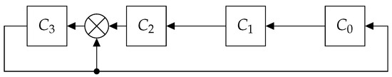
Figure 1.
Linear feedback shift register with underlying polynomial over in Galois configuration.
The underlying characteristic polynomial that prescribes the structure of the shift register in this example is over the finite field . As shifts are performed on the register, it traverses the states, as illustrated in Table 1. The initial state has been chosen to be of the form , which will be very convenient, as will be seen. It can be seen that the polynomial generates a maximum-length shift register sequence, as all non-zero states are included. Polynomials which fulfil the maximum-length property are known as primitive and it can be shown that such polynomials exist for every degree of polynomial [1,6].

Table 1.
LFSR states for polynomial .
The polynomial in the example contains only a single non-zero term apart from the leading and constant term; therefore, it requires only a single two-input XOR gate and four flip–flops due to its degree, making it particularly suitable for high clock speeds. Such hardware-friendly trinomials can be primitive, as in this example; however, there does not exist a primitive trinomial for every polynomial degree. In these cases, primitive polynomials with more than three terms can be selected, or trinomials with a shorter period can be employed. Alternatively, higher degree trinomials could be used that satisfy the required period constraints.
For a characteristic polynomial
of degree w, the state transformation matrix of the LFSR can be constructed as
It follows that a single shift on the register with initial state can be expressed as
An interesting property of LFSRs is that their operation is reversible as long as the characteristic polynomial has a constant term of one. The constant term of one is a prerequisite as otherwise the value of the most-significant register bit would not be recoverable after a performed shift due to loss of information. An alternative explanation is that matrix F would not be invertible if . To obtain the LFSR operating in reverse, the horizontal arrows in Figure 1 simply need to be inverted, as shown in Figure 2.
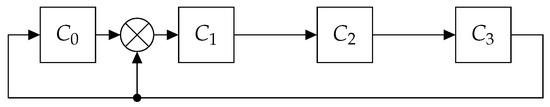
Figure 2.
Linear feedback shift register with underlying polynomial over in Galois configuration.
As shifts are performed on this reversed LFSR, it traverses through the same cycle of states as shown in Table 1; however, this time in opposite order. The characteristic polynomial of this LFSR is and the relationship between and is given by . In other words, is the reciprocal polynomial of . In what follows, only characteristic polynomials with constant term are considered.
Each state of an LFSR sequence that is generated by a polynomial , where , has not only a unique successor, but also a unique predecessor as can be easily deduced. The uniqueness of successors can be readily seen from (1), while the uniqueness of predecessors is determined through (it is guaranteed that F is invertible due to ). With the selection of as the initial LFSR state, the uniqueness properties prescribe that the obtained sequence of states will repeat after a certain number of shifts. As long as this period is greater than the maximal count that is to be supported, the characteristic polynomial is suitable for operation. For example, if counter states up to are to be supported, the period needs to be at least 15.
Furthermore, if the LFSR is continuously shifted from its initial state , the single one on the right-hand side will slide across to the left-hand side until state is reached. In Table 1, this subsequence starts with state and ends with state . This is the maximal number of shifts required after which a one will appear at the most significant bit position of the shift register. The number of shifts equals one less than the degree w of the characteristic polynomial (), since the degree prescribes the length of the shift register. Starting from any other state, fewer shifts will be needed. As can be easily seen, after each of these shifts, the least significant bit position of the shift register equals zero (states to ).
The state that follows always corresponds to the trailing coefficients of the characteristic polynomial, for the only one that gets shifted out feeds back at exactly the tap positions according to the polynomial. Specifically, this state can be indicated as
In the example, the state corresponds to . It can be seen that the least significant bit of this state is always one since . In summary, for sequences generated by polynomials with , the maximal number of consecutive states where the least significant bit is zero, equals one less than the degree w of the polynomial, and these states directly follow state .
4. Programmable Counter Overview
This section gives a brief description of the operation of the synchronous programmable counter. The top-level schematic of the counter with all its inputs and outputs is shown in Figure 3. It serves as the basis for the different implementations proposed in the following sections.
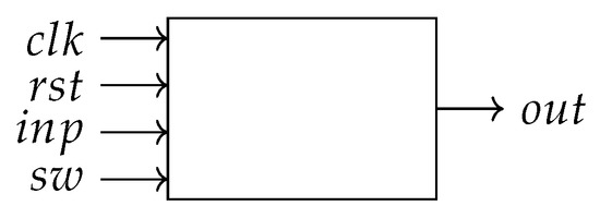
Figure 3.
Programmable counter top-level schematic.
At its core, each counter architecture accommodates an LFSR sized to w bits, as shown in the example in Figure 1. To enable the counter operation, input needs to be pulsed for a single clock cycle and, in the following w clock cycles, the desired binary counter value b needs to be fed into input , starting from the least significant bit. Subsequently, the counter undergoes a conversion phase in which the binary sequence value b is encoded internally into a corresponding LFSR sequence state . Once complete, the counter starts continuously decrementing from state to . Each time state is reached, a pulse is output on . Should the counter be configured with , a pulse is issued in every clock cycle, i.e., stays always high. Thus, the counter supports the full range where . The operation of the counter can be stopped by pulsing again.
In the described deployment, the counter is decrementing in each clock cycle, and the overall circuit can thus be considered a timer. In general, however, it is possible to synchronise the decrement operation with the occurrence of specific other events. The circuit can thus be used for a variety of applications that are not limited to measuring time durations.
5. Fast End of Count Detection
A crucial element in realising high-speed LFSR counters is an efficient method for detecting the end of count (EOC). The EOC detection for programmable counters in previous works does not scale with the counter width, and thus, becomes the speed limiting element. Methods for speed recovery typically spread the detection over several clock cycles at the expense of usable counter periods. In the following, a method for LFSR counters is presented that allows for high scalability without sacrificing speed or counter range.
The proposed LFSR counters in this paper decrement continuously from an automatically converted state down to . Each time the zero state is encountered, the counter needs to be reloaded with . Additionally, the conversion algorithm described in Section 8 requires the detection of state . The proposed circuit for detecting the zero state is shown in Figure 4.
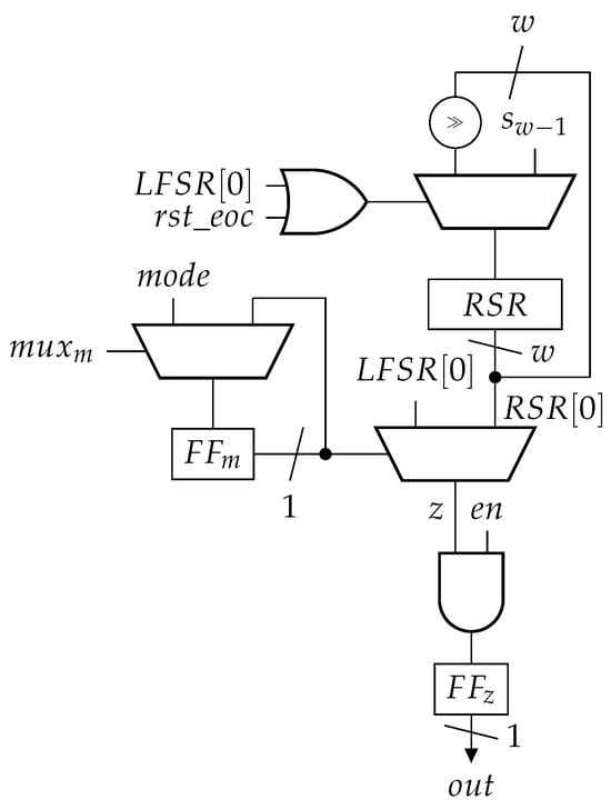
Figure 4.
End of count (EOC) detection logic (also referred to as zero-detection logic) for the proposed recursive and iterative counter circuit implementations.
The multiplexer inputs are addressed from left to right starting with 0. It is assumed that an LFSR of width w (an example is shown in Figure 1) is at use in conjunction with the EOC detection logic. The EOC detection works in one of two modes as determined by the state of flip flop , which is controlled by . Mode 0 () is used as long as . In this case, the zero state is simply detected through the least significant bit of the LFSR (). It is known that the state is reached when , for for any state , where , as detailed in Section 3.
Mode 1 () is used in cases where . In this mode, the zero state is detected after consecutive zeros have been observed at the least significant bit of the LFSR. This works for the longest sequence of zeros is observed as states to are traversed. The detection of the sequence of zeros is accomplished with shift register . Each time a one is encountered at the least significant bit position of the LFSR, shift register is reset to state . In all other cases, a shift is performed on moving the one closer towards its least significant bit. Once , it must be that . Therefore, in mode 1, the zero state is detected through a one on . The operation of the zero-detection logic in mode 1 is visualised in the state diagram shown in Figure 5.
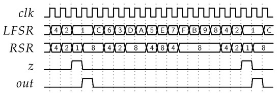
Figure 5.
Timing diagram showing how the state extension is achieved for a 4–bit wide LFSR counter using the proposed EOC detector circuit in mode 1. The counter period in this example has been set up to 16 (). It can be seen that LFSR state always appears in two consecutive clock cycles. The first occurrence corresponds to , whereas the second one refers to , which is identical to due to the LFSR sequence wrapping around. The EOC detector correctly identifies only the first occurrence as a zero.
Signal can be used to reset for initialisation and can be driven by a one-hot-state machine flip–flop of the programmable counter. The wide multiplexer disappears if the OR gate is connected to set/reset the register bits of and the AND gate is also superfluous since the inverted signal of (driven by a flip–flop) can be directly connected to the reset of . Signal can directly drive the enabling of . Overall, the EOC detector can be realised with a single level of logic.
6. State Extension
The maximum-length sequence of an LFSR does not include the state with all bits equal to zero. Nonetheless, the proposed LFSR counters achieve periods of length . The method behind this state extension is illustrated using the polynomial and its corresponding states from the example in Table 1. If binary value (equivalent to a period of length 16) is converted into its corresponding LFSR state, the encoding procedures that will be presented in the following sections simply lead to state since the sequence wraps around after state . Then, by using LFSR state for the counting procedure, it is necessary to distinguish between a period length of 1 and 16, which both map onto . The distinction is achieved through the mode of the zero detection circuit. Recall that the zero detection mode is equal to 0 for , and 1 otherwise.
Figure 5 shows a timing diagram for the operation of one of the proposed counters using a period length of 16. When the end of the sequence is detected with signal z going high, it can be seen that, in the following clock cycle, the LFSR counter is reloaded with and is reset to . Because the zero detection circuit is operated in mode 1, z lowers to 0 since it mimics, in this mode, the LSB of . From state , the sequence wraps to and decrements all the way to , at which point z goes high again due to the LSB of finally becoming one. In this way, a period length of 16 is achieved using an LFSR of degree four.
With the described technique, a maximum-length LFSR sequence can be extended by a maximum of states. Extending beyond one state, however, will require an increase in the width of the binary value b. For completeness, it needs to be noted that, alternatively, longer periods can also be obtained by increasing the width of the LFSR counter. If no more than additional states are required, however, the proposed state extension in this section is preferred since it comes with no additional cost.
7. Recursive LFSR Encoding
An algorithm to encode binary values into their corresponding LFSR state using the principle of superposition has been previously used in the software domain [9,10]. In Section 7.1, this algorithm is mathematically derived using a different approach. An efficient hardware implementation is proposed in Section 7.2, where a first programmable LFSR counter is also obtained.
7.1. The Recursive Algorithm
To illustrate the operating principle of the algorithm, generator polynomial of degree is selected as an example and the corresponding states tabulated in Table 2 are considered.
Table 2.
LFSR states used for encoding binary values using the principle of superposition.
The first row contains all the possible initial states of the LFSR with only a single bit set. The particular states are to . Within each column, the states that follow the initial state after steps in the LFSR sequence are shown, where . The values within a row can be easily calculated from the rightmost state, as going from right to left in the table is equivalent to single shift operations on the LFSR. A state in the rightmost column can be obtained recursively from values in the previous row using the principle of superposition. With the LFSR transformation matrix F and the fact that any LFSR state can be decomposed into a linear combination of the initial states to , the state can be expressed as
Thus, is a linear combination of the states to , which are just the states of the previous row. The elements of , which are expressed as , indicate which states are part of the linear combination. An alternative way to express this is
As an example, to obtain state , state needs to be considered. Its elements indicate that can be calculated as
To encode a binary counter value b into its corresponding LFSR state with the help of the derived relationships, the following transformation is used:
As b is decomposed into its powers of two
it follows that
The expression can be evaluated by first obtaining for the smallest j, where . As previously described, is just a composition of the states , which correspond to a row in Table 2. The obtained value can then be multiplied with the next transformation matrix in line, until all non–zero coefficients of b have been processed.
As an example, is to be calculated using the algorithm derived. Since 12 can be decomposed into powers of two as , it follows that
7.2. The Recursive Circuit
An implementation of a programmable LFSR counter based on the encoding algorithm derived in Section 7.1 is presented in this section. The top–level counter schematic is shown in Figure 3 and described in Section 4. It is assumed that a generator polynomial of degree with a non-zero constant term has been selected such that its period length supports the desired maximal counter value. Upon the activation of the counter (via ), the binary counter value b needs to be presented bit by bit at the input so that it can be shifted into a shift register , which is depicted in Figure 6.
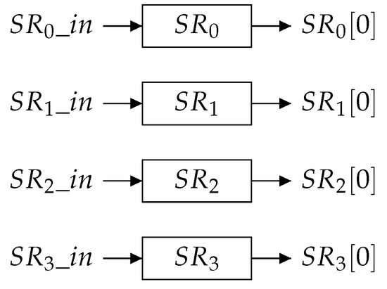
Figure 6.
Auxiliary shift registers of width w used by both the recursive and the iterative counter circuit implementations.
Subsequently, the counter will perform a setup procedure in which the binary counter value is converted into the corresponding LFSR state . Once this is complete, the counter will continuously be loaded with and count down to , until is pulsed again for deactivation. Whenever the counter reaches , this is signalled at the output with going high.
The core part of the counter circuitry is shown in Figure 7.
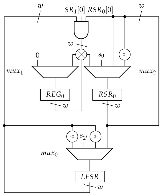
Figure 7.
Programmable LFSR counter based on the recursive conversion algorithm.
This is to be used in conjunction with the fast EOC detection circuit from Figure 4, which is described in more detail in Section 5. Where single-bit and multi-bit signals are combined in a logic gate in circuit diagrams, the logic gate is to be widened to match the size of the multi-bit signal, and the single-bit signal is to be replicated for each bit position. Symbol ≫ denotes a right shift on an ordinary shift register and a forward shift on an LFSR where the state is advanced from to . In contrast, symbol ≪ denotes a backward shift on an LFSR where state decrements to state . It should be noted that many of the multiplexers in the drawn circuits can be absorbed into flip–flop clock enable and set/reset logic.
The is the main component in the circuit, and it is wired to the generator polynomial and also to the reciprocal polynomial of . It can, therefore, shift forward and backward, as also indicated by the settings of the upstream multiplexer. For the conversion phase, the is initially loaded with state corresponding to the rightmost state in row 2 of Table 2. In consecutive clock cycles, the is shifting forward, traversing the entries in the table from right to left. Once the leftmost state of a row is reached, the rightmost state from the next row is loaded. The proposed method to calculate the rightmost states () is presented later.
The matrix–vector multiplications in (3) are accomplished through register and the loadable shift register . Initially, is reset to 0, while is loaded with . As shifts to the right, its least significant bit, together with the least significant bit of (which holds a value ), is used to determine which columns of the matrix, and thus, which states of the , need to be accumulated inside . The final value of the product is saved into for the next multiplication to be performed, if a subsequent one is to be scheduled. Once the entire expression (3) has been evaluated, the conversion is complete, and the result is held in . From this moment on, can be loaded with this value and the count down procedure can start by operating the LFSR in backward mode.
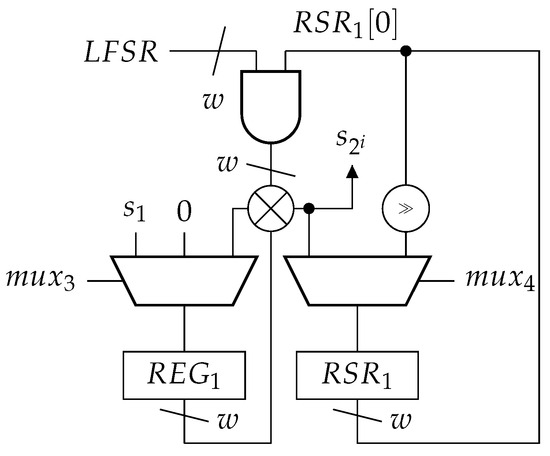
Figure 8.
Auxiliary circuit for the recursive counter implementation to calculate the states using the recursive algorithm itself.
It calculates the values using (2) and works similarly to how the main circuit in Figure 7 is used to perform matrix–vector multiplications. Shift register is initially loaded with the first state from through the XOR gate. At the start of the computation, is reset to 0 to accumulate the needed values of according to the least significant bit of . After w clock cycles, contains state . This procedure is then continuously repeated until the remaining states to have been produced.
As an example, value is to be converted into its corresponding LFSR state . Table 3 shows the contents of the relevant registers in each clock cycle of the conversion.
Table 3.
Example counter value conversion for the recursive LFSR counter implementation.
As can be seen, shift register is initially loaded with value . After each clock cycle, is shifted by one position, when the processing of its least significant bit has completed. It can be seen that is loaded at the start of every clock cycles with the relevant state . In subsequent clock cycles, is simply advancing its state. essentially traverses the states tabulated in Table 2 from right to left and from top to bottom. The two multiplications that take place in parallel can be observed in register pairs, (,) and (,). Once all non–zero bits of have been processed, the result of the conversion is contained in . At the end of the conversion, the register holds state as expected.
The state machine of the entire circuit is presented in Figure 9, while the different control signals are listed in Table 4.
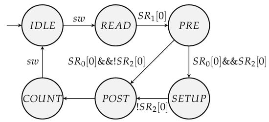
Figure 9.
State machine for recursive and iterative counter circuit implementation.
Table 4.
Control signals for the recursive LFSR counter implementation.
Empty cells in the table indicate don’t–care values. They help in optimising the logic but should be otherwise fixed so that power consumption is reduced. For each multiplexer, the inputs are addressed from left to right starting with 0. The different states of the counter and the functions of the circuit components are described in more detail in the following:
- IDLE:
- In this state, the counter is inactive and waiting for a pulse on input . Once a pulse is received, the system transitions into the READ state and, at the same time, a one is shifted into shift register .
- READ:
- This state is executed for a total of w clock cycles. In each clock cycle, a zero is shifted into to clear this register, as it may still contain some non-zero bits from the previous run. An exception is the last clock cycle, in which a one is shifted into . During this state, the binary counter value b is also read in serially through and shifted into . Each time a one is shifted into , a one is also shifted into to keep track of the present non-zero bits in b. During power-up, the shift register is initialised to value and is rotated in each clock cycle of this state. Each time the least significant bit of is differing from , the mode of the zero-detection logic is updated to the inverted value of . This procedure is essentially a serial comparison between b and , and ensures that the zero-detection mode is programmed to 0 only if , and otherwise to 1. Shift register is cleared by shifting out any one it may store, and is reset to . After clock cycles, the one that was shifted into in the IDLE state appears at the least significant bit position and signals the last clock cycle of the READ phase. For the next clock cycle, the state machine transitions into the PRE state.
- PRE:
- This state is also executed for a total of w clock cycles and is mainly used to shift any ones that might have been shifted in the previous phase into , to its least significant bit positions. The shifting stops should be . Furthermore, register is reset to 0, whereas shift register is reset to . is kept at except for the last clock cycle in which it is also reset to 0. and are both reset to through . The end of the state is reached once a one appears at the least significant bit of . In the last clock cycle, indicates whether b is non-zero as in this case , otherwise . Should , the conversion phase is complete, as has already been reset to the corresponding state . In this case, the next state is POST, otherwise a conversion is initiated by transitioning into state SETUP. In an alternative implementation, the PRE phase could also terminate as soon as a one reaches the least significant bit of , at the expense of more complex control logic.
- SETUP:
- This phase requires a minimum of and a maximum of clock cycles, depending on the value b that is to be converted. Table 2 is traversed from left to right and from top to bottom and necessary values accumulate for as long as there is still an unprocessed non-zero digit of b inside . Each digit in corresponds to a row in the table. is used as in the previous phase to detect each time w clock cycles have elapsed and a digit of b, and thus, a table row has been processed. When a row has been processed, is reloaded with the next in sequence, and are reset back to zero, and and are loaded with their respective matrix–vector product. Moreover, a shift is performed on to move the next bit of b into place. If the bit that was shifted out was a one, a shift is also performed on , since it keeps track of the unprocessed ones. In all other clock cycles, and accumulate their partial product, while and shift right and advances its state. Once all non–zero digits of b have been processed, an additional clock cycle is used in which the corresponding condition is detected for transitioning into the POST state. This last clock cycle could also be eliminated, but it was found that it led to less complex control logic and better timing.
- POST:
- This state lasts only a single clock cycle and is used to preload the LFSR with the converted value that is found inside . Shift register , that is used as part of the zero-detection logic, is also reset in this state to as the transition happens into the COUNT state.
- COUNT:
- Once this state is reached, the LFSR is operated in backward mode where it is continuously counting down. The zero-detection logic signals the occurrence of state . In this case, the LFSR is reloaded with from . The procedure continues until a pulse is detected on , in which case the counter transitions back into its IDLE state.
8. Iterative LFSR Encoding
In Section 8.1, a second and new algorithm to encode a binary value b into its corresponding LFSR state is presented. The algorithm is a modified version of the iterative method that avoids the use of slow binary counters to keep track of the number of needed shifts. Subsequently, in Section 8.2, an efficient hardware implementation of this algorithm is proposed that leads to a second programmable fast LFSR counter.
8.1. The Iterative Algorithm
A generator polynomial with a non-zero constant term is selected, such that the desired maximal counter value is supported by the period of the polynomial. For the encoding procedure of the counter value, three LFSRs are used in conjunction: is the main component and is wired to the reciprocal polynomial of , thus, it is always counting down, whereas and are both wired to itself to count up.
A binary counter value b, that is to be converted into LFSR state , is loaded into an ordinary shift register . is initialised to state and keeps counting up in its sequence of states in every step of the algorithm. In contrast, is initialised to state and keeps counting down. However, whenever reaches the state , it is loaded with the current state of . With this rule, starts with its initial state of , then is loaded in the next step with state and counts down to , then from to , then from to , and so on. Thus, with each reload of , the number of steps to reach the zero state again doubles.
Each time is in its zero state , a shift is performed on shift register , such that its least significant bit is shifted out of the register. This means that each bit of is present at the least significant bit position of for the duration of its corresponding power of two . Initialising to and incrementing it every time a one is present at the output of shift register will ensure that holds state in the end since .
An example is illustrated in Table 5, where the binary counter value is converted into its corresponding state .
Table 5.
Example counter value conversion for the iterative LFSR counter algorithm.
It can be seen that is counting up in every step, whereas is counting down sequences from to , starting from . is only advancing at times when . The conversion finishes when all ones have been consumed from . Specifically, the algorithm requires steps of processing. In the best case, it requires only one step, whereas in the worst case, it requires a total of steps. Once a conversion is complete, can be loaded with the converted state of and can start counting down until state has been reached at which point it can be reloaded again.
8.2. The Iterative Circuit
In this subsection, an efficient fast circuit implementation of a programmable LFSR counter based on the iterative conversion algorithm from Section 8.1 is presented. It is assumed that a polynomial with a non-zero constant term and degree has been selected. The top-level schematic of the system with its inputs and outputs is shown in Figure 3 and described in Section 4, while the state machine is depicted in Figure 9.
The core part of the counter is detailed in Figure 10.
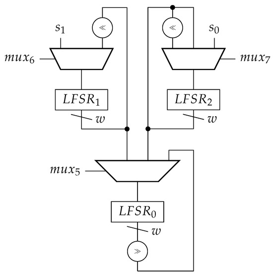
Figure 10.
Programmable LFSR counter based on the iterative conversion algorithm.
The three LFSRs, as described in Section 8.1, are shown. Many of the multiplexers in the drawn circuit can be absorbed into flip–flop clock enable and set/reset logic. Additionally, the fast EOC detection logic from Figure 4 is employed to detect whenever the zero state is present in . Four needed auxiliary ordinary shift registers, that are not required to be loadable, are shown in Figure 6. The control signals of the counter are detailed in Table 6.
Table 6.
Control signals for iterative LFSR counter implementation.
Empty cells in the table indicate don’t–care values and help with logic minimisation; otherwise, they should be fixed so that power is saved. With respect to the control signals, the inputs for each multiplexer in Figure 4 and Figure 10 are addressed from left to right starting with 0.
The various states of the system and the functions of the different components are described in more detail in the following:
- IDLE:
- The system is waiting for a start pulse on the input . Once a pulse is observed, the system shifts a one into and transitions into state READ.
- READ:
- This state is executed for a total of w clock cycles. In every clock cycle, a zero is shifted into and to clear both of them should they still contain any ones from the previous run. Also, in every of the w clock cycles, a bit from the binary counter value b is read in through the input and shifted into . Whenever a one is shifted into , a one is also shifted into to keep track of the number of ones inside . In the last clock cycle of this state, the one that was shifted in the IDLE state into appears at its least significant bit position and triggers a transition into state PRE.
- PRE:
- The pre-setup phase lasts for a total of w clock cycles. It is mainly used to shift any ones inside to the least significant end of the register. All three LFSRs are preloaded with their required initial values for the conversion algorithm. and are directly loaded with and , respectively. is initialised with through . The zero-detection mode is reset to 0. Once the one that was shifted in the READ state into reaches the least significant bit position of the register, the PRE phase completes. If , it follows that in the last clock cycle of this phase and a transition is directly made into the POST state, because has already been preloaded with the converted value . In all other cases, , since there will be at least a single one present in b, and thus, the conversion algorithm needs to be initiated by transitioning into the SETUP phase next. In the last clock cycle, a new one is also shifted into .
- SETUP:
- The length of this phase depends on the counter value b that is to be converted and lasts specifically clock cycles. During this state, is advancing in every clock cycle, whereas is only advancing for as long as . A one is shifted into in every clock cycle until it saturates, to keep track of the shifts that have been performed on . In the same way, is used to keep track of the number of shifts performed on . Whenever the zero-detection logic signals that has reached (), a shift is performed on to shift out the processed bit and move to the next binary digit. If a one is shifted out of , a shift is also performed on to shift out its corresponding one. At the same time, is reloaded from and the zero-detection mode is updated with the value of , which is high if is in a state with . Once the least significant bit of is zero, all ones inside have been processed and the setup phase is terminated by switching to the POST state.
- POST:
- During the post-setup clock cycle, is preloaded with the converted state that is present in . The required zero mode for this LFSR state is held inside so that is also updated to this value. Lastly, is reset to .
- COUNT:
- In this phase, starts counting down starting from . Once it reaches state , it gets reloaded with from and the counting resumes. Additionally, output is pulled high during this time. This phase terminates and a transition is made back to the IDLE state once a pulse is registered on .
9. Results
This section presents and compares FPGA and ASIC implementation details for the two proposed circuits: the recursive circuit from Section 7 and the iterative circuit from Section 8. Additionally, the closest state-of-the-art solution [11] has been recreated and implemented, targeting the same technologies for a direct comparison. For the state-of-the-art design, it was necessary to specify multi-cycle paths for the subtractor unit as proposed by the authors. It was found that three clock cycles were sufficient to prevent these becoming critical paths for the design. Also included in the comparison is an ordinary binary counter.
All circuits have been built around the interface shown in Figure 3 and simulated for counter sizes between 2 and 64 bits. For the proposed LFSR–based solutions, for a given size of counter, a primitive trinomial has been selected whenever existent and, otherwise, a primitive polynomial with the least number of terms has been used for reduced hardware complexity. Power numbers have been obtained by setting up the counters with value and letting them run for 1 ms. Where counter sizes are smaller, only the corresponding least significant portion of the counter value is loaded.
Besides the maximal achieved frequency, area, power consumption, and trade-off parameters such as the ADP (area-delay product) and PDP (power-delay product), the following metrics are used for evaluation:
- Levels of logic: The maximal number of LUT cells (basic building blocks for logic) required on any timing path between two sequential cells on the FPGA. The levels of logic is one factor influencing the lower bound of the achievable frequency.
- FPGA slices: A slice is a resource on an AMD FPGA [38] that is used to implement sequential or combinatorial circuits. On 7 Series AMD FPGA devices, a slice contains four six-input LUTs, eight storage elements, carry lookahead logic, and wide-function multiplexers. The number of required slices indicates the resource utilisation.
- Worst-case conversion clock cycles (latency): For the proposed solutions, there is an initial configuration phase required to convert the binary period into an LFSR sequence state before the counting procedure starts. This conversion time depends on the value that is to be converted. To obtain an upper bound on the latency, the worst-case scenario is considered.
9.1. FPGA Implementation
All circuit designs have been implemented for each single counter width between 2 and 64 bits targeting an Artix–7 35T FPGA device of speed grade −1 L manufactured by AMD, Santa Clara, CA, USA, and using the AMD Vivado Design Suite v2022.2.
The required levels of logic for all the circuits are plotted in Figure 11.
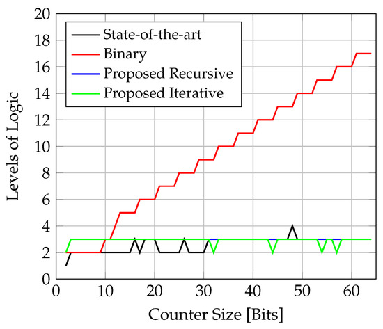
Figure 11.
Comparison of required number of logic levels for counter implementations on FPGA. The multi-cycle paths of the state-of-the-art counter have not been included in the number of logic levels to not mask the core logic.
It can be seen that, as the counter width increases, the levels of logic also increases for the binary circuit. The binary counter uses a chain of dedicated fast lookahead carry logic, whereby the critical path grows linearly with w [38] For every group of four bits, the logic depth increases by an additional CARRY4 chain element. For the state-of-the-art counter, the multi-cycle paths of the subtractor have not been included in the calculation of the logic levels so as not to mask the complexity of the main logic. The design solves the carry propagation limitation of an ordinary binary counter, but its EOC detection mechanism grows logarithmically in terms of levels of logic as the counter is scaled up. Nevertheless, the instance for still requires only three levels of logic to combine all 64 comparator signals as the FPGA offers six-input LUT cells. In one instance, the tool already defaulted to using four levels of logic (). The proposed recursive circuit has been implemented with a maximum of three levels of logic. The big advantage is that the levels do not increase further as the logic depth is independent of the counter width. The iterative circuit shows even better behaviour as several instances of it could be implemented with only two levels of logic, which means that it should be possible to attain two levels of logic for all instances due to the independence of the counter size; this could be achieved through an explicit low-level coding of the state machine.
In Figure 12, the achieved frequencies are plotted for all the designs.
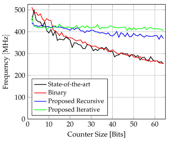
Figure 12.
Comparison of achieved frequency for counter implementations on FPGA.
The proposed circuits achieve frequencies in the range of 400 MHz, while the iterative circuit shows the best performance overall with an average of MHz. The frequency of the binary counter continually decreases to MHz. This comes as no surprise, as the critical path grows with the size of the counter. Interestingly, the state-of-the-art counter also continuously decreases in frequency and even underperforms the binary counter in many instances. Even though the levels of logic do not exceed four for the considered counter instances (omitting multi-cycle paths), the performance degradation comes down to routing complexity. A more guided placement methodology for this counter architecture might lead to better results.
The resource utilisation in terms of number of FPGA slices is shown in Figure 13.
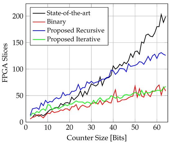
Figure 13.
Comparison of slice utilisation for counter implementations on FPGA.
The iterative circuit and the binary counter show very similar linear behaviour and, also, the overall lowest utilisation of all the solutions. The utilisation for the recursive solution also grows linearly, but at a higher slope. The hardware costs for the proposed solutions scale linearly with w, because the degree directly prescribes the width of all the multi-bit registers and the corresponding logic cells in the designs. Due to the matrix structure of the state-of-the-art design, its hardware resources grow quadratically. For , the number of required slices exceeds those of all the other solutions.
The dynamic power consumption can be seen in Figure 14 and is based on simulations with a clock period of ns.
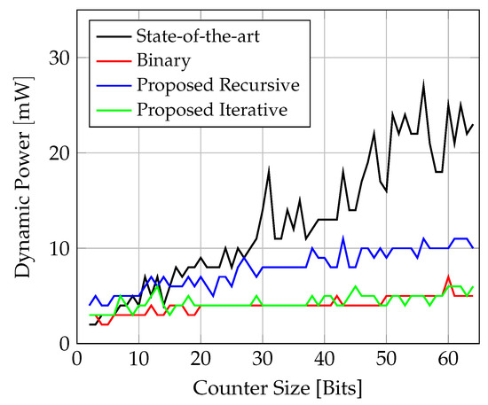
Figure 14.
Comparison of dynamic power consumption for counter implementations on FPGA.
The tool reports static power only for the entire FPGA device which is, in all cases, 62 mW.
The ADP (area-delay product) and PDP (power-delay product) compound metrics are shown in Figure 15 and Figure 16, respectively. The area for the ADP is estimated using the number of slices as reported in Figure 13, and, for the PDP, the dynamic power from Figure 14 is used. For both metrics, it can be seen that, as the width is scaled up, the iterative design performs best, followed by the binary counter, the recursive solution, and then the state of the art.
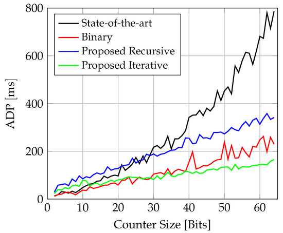
Figure 15.
Comparison of ADP (area-delay product) for counter implementations on FPGA.
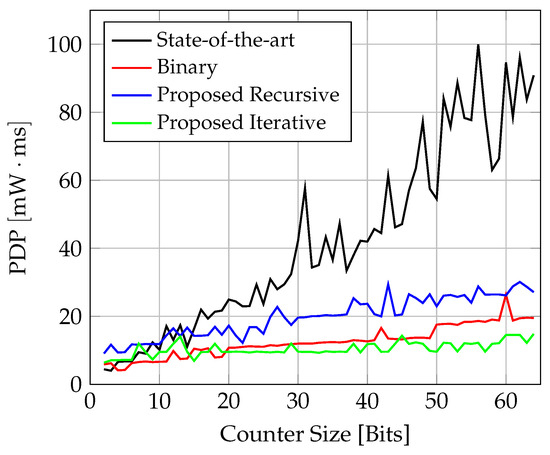
Figure 16.
Comparison of PDP (power-delay product) for counter implementations on FPGA.
9.2. ASIC Implementation
All the designs have been simulated targeting TSMC’s N3 process node (N3B) with a mix of LVT, LVTLL, ULVT, and ULVTLL standard cells using Synopsys Fusion Compiler version R–2020.09–SP6. A stack of 19 metal layers has been used. The results are reported for a typical process corner with an operating voltage of V and a temperature of 85 °C. The counter sizes w have been incremented in steps of four bits, where . Only relative numbers are provided, as absolute numbers are subject to confidentiality restrictions.
The plot in Figure 17 shows the maximal achieved frequencies relative to each other.
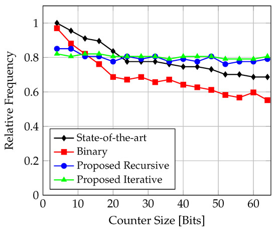
Figure 17.
Comparison of achieved frequency for counter implementations targeting TSMC N3 CMOS technology.
It can be seen that the lowest frequencies are attained by the binary counter for . With the flexibility offered by an ASIC, the routing complexities of the state-of-the-art design seen on the FPGA are no longer the decisive factor in this comparison. The design outperforms all other designs for , but then starts dropping in performance. The proposed solutions always outperform the state-of-the-art design for . The iterative and recursive solutions behave very similar to each other and show a fairly constant speed as the counter is scaled up.
The total cell areas relative to each other are graphed in Figure 18.
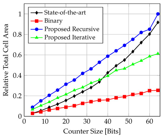
Figure 18.
Comparison of total cell area for counter implementations targeting TSMC N3 CMOS technology.
As is the case with the FPGA implementation, all the proposed solutions and the binary counter show fairly linear resource requirements. The cell area of the state-of-the-art solution grows quadratically, as is the case when targeting the FPGA. Overall, the recursive solution requires the most area (up to ), while the binary counter is the most economical. The iterative solution lies between the recursive and the binary solutions.
In Figure 19, the total power consumptions relative to each other are shown.
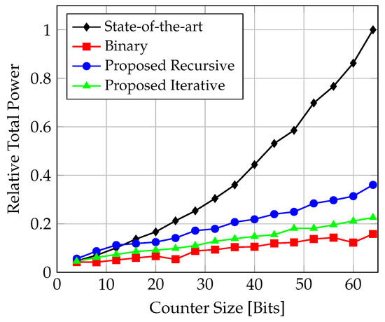
Figure 19.
Comparison of total power consumption for counter implementations targeting TSMC N3 CMOS technology.
The state-of-the-art solution is the most power-hungry design, while the binary counter is shown to be the most economical. Similar to the binary counter, the proposed solutions show fairly linear behaviour, albeit with a slightly higher slope.
The relative ADP (area-delay product) and PDP (power-delay product) are shown in Figure 20 and Figure 21, respectively. For both compound metrics, the binary counter shows the overall best trade-off. In general, the iterative solution shows better behaviour than the recursive one. Regarding the PDP, the iterative solution is even very closely aligned with the binary counter. Up to , the state-of-the-art solution shows a better ADP than the proposed solutions, but then is outperformed by the iterative design, and with also by the recursive one. For , the state-of-the-art design exhibits the worst PDP.
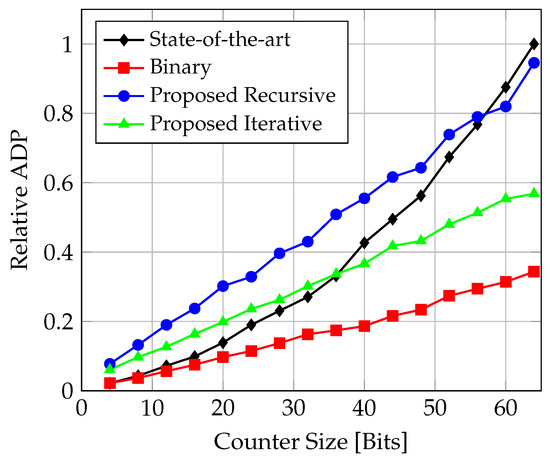
Figure 20.
Comparison of ADP (area-delay product) for counter implementations targeting TSMC N3 CMOS technology.
Figure 21.
Comparison of PDP (power-delay product) for counter implementations targeting TSMC N3 CMOS technology.
9.3. Programming Considerations
An important aspect for all the counter designs concerns the required time for the encoding of desired counter values into a format suitable for operation. The big advantage of the binary counter circuit is that it can directly load a binary counter value and start counting. The state-of-the-art circuit [11] also does not require any encoding procedure; however, due to its multi-cycle paths, a few clock cycles are necessary each time a new counter value is set up. For the proposed LFSR solutions, the counter value needs to be converted into an LFSR state first. The time required for conversion is calculated as follows:
For reduced control logic complexity, has been fixed to be w for the two LFSR circuits. The minimal conversion time of w clock cycles is achieved for , because, in this case, the SETUP phase is skipped. The SETUP time can be specified for the recursive circuit as
and for the iterative circuit as
Therefore, the time complexity of the conversion algorithm for the recursive circuit is quadratic in w, whereas it is exponential for the iterative approach. The worst-case encoding latencies in terms of number of clock cycles are visualised in Figure 22.
Figure 22.
Comparison of worst-case encoding latencies in terms of clock cycles for counter implementations.
For and an operating frequency of 5 GHz, for instance, the iterative approach would require 859 ms for the worst-case conversion, while it could be accomplished with the recursive approach in only 211 ns. For either approach, there may be applications for which these conversion times are acceptable. The worst-case conversion time can also be reduced by restricting the maximal supported counter value.
A summary of the characteristics for the different counter architectures is shown in Table 7.
Table 7.
Comparison between different proposed programmable counter implementations.
It can be seen that the state-of-the-art design has a restricted counter range, while the proposed solutions support the full range.
10. Conclusions
A new method for detecting the end of count for LFSR counters has been proposed. Previous methods for detecting the end of count did not scale with the counter width; thus, they either limited the maximal frequency or, if the detection was spread over several clock cycles, limited the usable counter range. Both issues are solved with the new EOC circuit in conjunction with LFSR sequences. Based on this new EOC detector circuit, it is shown how maximum-length LFSR sequences can be easily extended by a number of states up to one less than the degree of the underlying polynomial. A novel iterative algorithm is proposed to encode a binary sequence value into its corresponding LFSR sequence state. This algorithm is a modification of the conventional iterative algorithm and uses a combination of three LFSRs to avoid the requirement of a binary counter to keep track of the number of shifts. Based on this new algorithm and an existing alternative recursive method, two novel programmable LFSR counter architectures have been proposed, in which each can be configured during runtime with a start count supplied as an ordinary binary value. The counters automatically encode the binary sequence value into the required LFSR state and, once complete, continuously count down from the start value and issue a signal each time the zero state is reached. Alternatively, the counters can be easily modified to decrement with the occurrence of an event rather than in every clock cycle. Applications are, for instance, clock dividers that need to be run at high clock frequencies.
The new counter designs are based on the LFSR, which requires the start count to be encoded into a corresponding LFSR state. In the past, different schemes trading off time and memory have been employed to perform a conversion, for instance, offline and then simply supply the converted value to the hardware counter. With the proposed architectures, the conversion can be accomplished by the hardware itself and even at a higher clock frequency than the state-of-the-art counter solution can operate when the counter width is scaled up.
All circuits, including the recreated state-of-the-art design [11], have been implemented on an FPGA and also simulated targeting TSMC’s N3 CMOS process. Some notable differences have been observed between the FPGA and ASIC implementations. For instance, the state-of-the-art design degrades in frequency due to routing complexities seen on the FPGA as the width increases; in many instances, it even underperforms the binary counter. The same behaviour is not evident for the ASIC implementation due to the relatively high abundance of routing resources. The routing complexity is also very likely related to the relatively higher area demand for the state-of-the-art design on the FPGA in comparison to the ASIC; it may be that the routing complexities effect the logic to be replicated to a greater extent.
The proposed designs are fully synchronous, can be implemented using standard cells and dispense of any timing exceptions. Not only are the architectures easily portable across technologies, but they are also highly scalable as the logic depth is independent of the counter size. The algorithms behind the circuits enable programmability to a specific counter value in either quadratic or exponential time. The circuits exhibit very different properties in terms of speed, resources, and conversion time and, thus, may each be suitable for a different type of application. Overall, the iterative solution shows the best performance in terms of frequency, area, and power efficiency. If a faster conversion time is required, however, the recursive solution can be employed. The state-of-the-art solution is outperformed as the counter size increases.
Funding
This research received no external funding.
Data Availability Statement
Dataset available on request from the authors.
Acknowledgments
The author thanks Steve Furber for his helpful advice, Emmet Fealy for his expertise on tuning the physical flow, and Leon Cavanagh for his time in reviewing the manuscript. Furthermore, the author wishes to acknowledge the constructive comments and suggestions for improvement offered by the anonymous referees.
Conflicts of Interest
Author Martin Grymel was employed by the company Intel Deutschland GmbH. The remaining authors declare that the research was conducted in the absence of any commercial or financial relationships that could be construed as a potential conflict of interest.
References
- Golomb, S.W. Shift Register Sequences, 3rd ed.; World Scientific: Singapore, 2017. [Google Scholar]
- Wang, L.T.; Stroud, C.E.; Touba, N.A. (Eds.) System-on-Chip Test Architectures: Nanometer Design for Testability; Elsevier: Amsterdam, The Netherlands, 2008. [Google Scholar] [CrossRef]
- Li, S.; Chen, L.; Ying, L.; Ren, J.; Wang, Z. Demonstration and Comparison of On-Chip High-Frequency Test Methods for RSFQ Circuits. IEEE Trans. Appl. Supercond. 2023, 33, 1302206. [Google Scholar] [CrossRef]
- Peterson, W.; Brown, D. Cyclic Codes for Error Detection. Proc. IRE 1961, 49, 228–235. [Google Scholar] [CrossRef]
- Moon, S.; Park, S.; Lee, J.H.; Lee, Y. Rapid Balise Telegram Decoder with Modified LFSR Architecture for Train Protection Systems. IEEE Trans. Circuits Syst. II Express Briefs 2019, 66, 272–276. [Google Scholar] [CrossRef]
- Clark, D.; Weng, L.J. Maximal and near-maximal shift register sequences: Efficient event counters and easy discrete logarithms. IEEE Trans. Comput. 1994, 43, 560–568. [Google Scholar] [CrossRef]
- Bae, H.; Hyun, Y.; Kim, S.; Park, S.; Lee, J.; Jang, B.; Choi, S.; Park, I.C. High-Speed Counter with Novel LFSR State Extension. IEEE Trans. Comput. 2023, 72, 893–899. [Google Scholar] [CrossRef]
- Ajane, A.; Furth, P.M.; Johnson, E.E.; Subramanyam, R.L. Comparison of binary and LFSR counters and efficient LFSR decoding algorithm. In Proceedings of the 2011 IEEE 54th International Midwest Symposium on Circuits and Systems (MWSCAS), Seoul, Republic of Korea, 7–10 August 2011; IEEE: Piscataway, NJ, USA, 2011; Volume 8, pp. 1–4. [Google Scholar] [CrossRef]
- Mrugalski, G.; Rajski, J.; Tyszer, J. Cellular automata-based test pattern generators with phase shifters. IEEE Trans.-Comput-Aided Des. Integr. Circuits Syst. 2000, 19, 878–893. [Google Scholar] [CrossRef]
- Mukherjee, N.; Pogiel, A.; Rajski, J.; Tyszer, J. High-Speed On-Chip Event Counters for Embedded Systems. In Proceedings of the 2009 22nd International Conference on VLSI Design, New Delhi, India, 5–9 January 2009; IEEE: Piscataway, NJ, USA, 2009; Volume 1, pp. 275–280. [Google Scholar] [CrossRef]
- Abdel-Hafeez, S.; Gordon-Ross, A. A Digital CMOS Parallel Counter Architecture Based on State Look-Ahead Logic. IEEE Trans. Very Large Scale Integr. (VLSI) Syst. 2011, 19, 1023–1033. [Google Scholar] [CrossRef]
- Hyun, Y.; Park, I.C. Constant-Time Synchronous Binary Counter With Minimal Clock Period. IEEE Trans. Circuits Syst. II Express Briefs 2021, 68, 2645–2649. [Google Scholar] [CrossRef]
- Lee, G.; Joo, B.; Kong, B.S. CMOS Clock-Gated Synchronous Up/Down Counter with High-Speed Local Clock Generation and Compact Toggle Flip-Flop. IEEE Trans. Circuits Syst. I Regul. Pap. 2023, 70, 5316–5327. [Google Scholar] [CrossRef]
- Chang, H.H.; Wu, J.C. A 723-MHz 17.2-mW CMOS programmable counter. IEEE J.-Solid-State Circuits 1998, 33, 1572–1575. [Google Scholar] [CrossRef]
- Lee, S.H.; Park, H.J. A CMOS high-speed wide-range programmable counter. IEEE Trans. Circuits Syst. II Analog. Digit. Signal Process. 2002, 49, 638–642. [Google Scholar] [CrossRef]
- Kuo, K.C.; Wu, F.J. A 2.4-GHz/5-GHz Low Power Pulse Swallow Counter in 0.18-µm CMOS Technology. In Proceedings of the APCCAS 2006—2006 IEEE Asia Pacific Conference on Circuits and Systems, Singapore, 4–7 December 2006; IEEE: Piscataway, NJ, USA, 2006; Volume 12, pp. 214–217. [Google Scholar] [CrossRef]
- Som, I.; Sarangi, S.; Bhattacharyya, T.K. A 7.1-GHz 0.7-mW Programmable Counter with Fast EOC Generation in 65-nm CMOS. IEEE Trans. Circuits Syst. II Express Briefs 2020, 67, 2397–2401. [Google Scholar] [CrossRef]
- Wang, Y.; Wang, Y.; Wu, Z.; Quan, Z.; Liou, J.J. A Programmable Frequency Divider with a Full Modulus Range and 50% Output Duty Cycle. IEEE Access 2020, 8, 102032–102039. [Google Scholar] [CrossRef]
- Kim, J. An N/M-Ratio All-Digital Clock Generator with a Pseudo-NMOS Comparator-Based Programmable Divider. Electronics 2022, 11, 261. [Google Scholar] [CrossRef]
- Abdel-Hafeez, S.; Harb, S.M.; Eisenstadt, W.R. High speed digital CMOS divide-by-N fequency divider. In Proceedings of the 2008 IEEE International Symposium on Circuits and Systems, Seattle, WA, USA, 18–21 May 2008; IEEE: Piscataway, NJ, USA, 2008; Volume 5, pp. 592–595. [Google Scholar] [CrossRef]
- Abdel-Hafeez, S.; Gordon-Ross, A. A Gigahertz Digital CMOS Divide-by-N Frequency Divider Based on a State Look-Ahead Structure. Circuits Syst. Signal Process. 2011, 30, 1549–1572. [Google Scholar] [CrossRef]
- Vaucher, C.; Ferencic, I.; Locher, M.; Sedvallson, S.; Voegeli, U.; Wang, Z. A family of low-power truly modular programmable dividers in standard 0.35-/spl mu/m CMOS technology. IEEE J.-Solid-State Circuits 2000, 35, 1039–1045. [Google Scholar] [CrossRef]
- Sheng, N.H.; Pierson, R.; Wang, K.C.; Nubling, R.; Asbeck, P.; Chang, M.C.; Edwards, W.; Philips, D. A high-speed multimodulus HBT prescaler for frequency synthesizer applications. IEEE J.-Solid-State Circuits 1991, 26, 1362–1367. [Google Scholar] [CrossRef]
- Lin, C.S.; Chien, T.H.; Wey, C.L. A 5.5-GHz 1-mW Full-Modulus-Range Programmable Frequency Divider in 90-nm CMOS Process. IEEE Trans. Circuits Syst. II Express Briefs 2011, 58, 550–554. [Google Scholar] [CrossRef]
- Kado, Y.; Ohno, T.; Harada, M.; Deguchi, K.; Tsuchiya, T. An ultralow power CMOS/SIMOX programmable counter LSI. IEEE J.-Solid-State Circuits 1997, 32, 1582–1587. [Google Scholar] [CrossRef]
- Gundla, A.R.; Chen, T. A low power frequency synthesizer for biosensor applications in the MedRadio band. In Proceedings of the 2015 IEEE 58th International Midwest Symposium on Circuits and Systems (MWSCAS), Fort Collins, CO, USA, 2–5 August 2015; IEEE: Piscataway, NJ, USA, 2015; Volume 5, pp. 1–4. [Google Scholar] [CrossRef]
- Chen, Z.; Zhang, Y.; Tang, X.; Li, J.; Huang, F.; Jiang, N. Design of Low Power Consumption, High-Speed and Wide Division Ratio Range Programmable Frequency Divider. In Proceedings of the 2020 IEEE 5th International Conference on Integrated Circuits and Microsystems (ICICM), Nanjing, China, 23–25 October 2020; IEEE: Piscataway, NJ, USA, 2020; Volume 10, pp. 289–292. [Google Scholar] [CrossRef]
- Tang, L.; Chen, K.; Zhang, Y.; Tang, X.; Zhang, C. A High-Speed Programmable Frequency Divider for a Ka-Band Phase Locked Loop-Type Frequency Synthesizer in 90-nm CMOS. Electronics 2021, 10, 2494. [Google Scholar] [CrossRef]
- Jiang, R.; Lei, Y.; Ye, S.; He, C.; Li, C.; Wang, W. A Low Phase Noise Programmable Divider Operating at 24 GHz in a 65-nm CMOS Technology. In Proceedings of the 2023 2nd International Joint Conference on Information and Communication Engineering (JCICE), Chengdu, China, 12–14 May 2023; IEEE: Piscataway, NJ, USA, 2023; Volume 5, pp. 95–99. [Google Scholar] [CrossRef]
- Zheng, Y.; Chen, X. A Low-Power RF Programmable Frequency Divider. In Proceedings of the 2023 8th International Conference on Computer and Communication Systems (ICCCS), Guangzhou, China, 21–23 April 2023; IEEE: Piscataway, NJ, USA, 2023; Volume 4, pp. 114–119. [Google Scholar] [CrossRef]
- Craninckx, J.; Steyaert, M. A 1.75-GHz/3-V dual-modulus divide-by-128/129 prescaler in 0.7-µm CMOS. IEEE J.-Solid-State Circuits 1996, 31, 890–897. [Google Scholar] [CrossRef]
- Larsson, P. High-speed architecture for a programmable frequency divider and a dual-modulus prescaler. IEEE J.-Solid-State Circuits 1996, 31, 744–748. [Google Scholar] [CrossRef]
- Morrison, D.; Delic, D.; Yuce, M.R.; Redoute, J.M. Multistage Linear Feedback Shift Register Counters with Reduced Decoding Logic in 130-nm CMOS for Large-Scale Array Applications. IEEE Trans. Very Large Scale Integr. (VLSI) Syst. 2019, 27, 103–115. [Google Scholar] [CrossRef]
- Ercegovac, M.; Lang, T. Binary counter with counting period of one half adder independent of counter size. IEEE Trans. Circuits Syst. 1989, 36, 924–926. [Google Scholar] [CrossRef]
- Stan, M.; Tenca, A.; Ercegovac, M. Long and fast up/down counters. IEEE Trans. Comput. 1998, 47, 722–735. [Google Scholar] [CrossRef]
- Levantino, S.; Romano, L.; Pellerano, S.; Samori, C.; Lacaita, A. Phase noise in digital frequency dividers. IEEE J.-Solid-State Circuits 2004, 39, 775–784. [Google Scholar] [CrossRef]
- Lacaita, A.L.; Levantino, S.; Samori, C. Integrated Frequency Synthesizers for Wireless Systems; Cambridge University Press: Cambridge, UK, 2007. [Google Scholar] [CrossRef]
- Xilinx. 7 Series FPGAs Configurable Logic Block—User Guide—UG474 (v1.8); Xilinx, Inc.: San Jose, CA, USA, 2016. [Google Scholar]
Disclaimer/Publisher’s Note: The statements, opinions and data contained in all publications are solely those of the individual author(s) and contributor(s) and not of MDPI and/or the editor(s). MDPI and/or the editor(s) disclaim responsibility for any injury to people or property resulting from any ideas, methods, instructions or products referred to in the content. |
© 2024 by the author. Licensee MDPI, Basel, Switzerland. This article is an open access article distributed under the terms and conditions of the Creative Commons Attribution (CC BY) license (https://creativecommons.org/licenses/by/4.0/).