Abstract
This paper presents the design and optimization of a small-size electromagnetic induction heating control system powered by a 3.7 V–900 mAh lithium battery and featuring an LC series resonant full-bridge inverter circuit, which can be used for small metal material heating applications, such as micro medical devices. The effects of the resonant capacitance, inductor wire diameter, heating tube material, and wall thickness were studied to maximize the heating rate of the workpiece and simultaneously reduce the temperature rise of the NMOS transistor. The optimal circuit configuration meeting the design requirements was finally identified by comparing the operational parameters and NMOS transistor loss under different circuit conditions. Validation experiments were conducted on designed electromagnetic induction smoking devices. The results indicate that under an output current of 4.6 A, the heating tube can reach the temperature target of 250 °C within 11 s, and all NMOS transistors stay below 50 °C in a 5 min heating process.
1. Introduction
Compared to traditional resistive heating, electromagnetic induction heating offers many advantages, such as high efficiency, rapid heating, precise power control, localized heating, and high safety due to its non-contact operation. Currently, induction heating applications are primarily adopted in high-voltage, large-scale heating equipment in metal processing industries, medical fields, and cooking devices, such as high-power metal smelting [1,2,3,4], household induction stove optimization [5,6,7], and the non-contact heating of internal metal implants [8,9,10].
In these large-scale devices, the electromagnetic induction heating control system is mainly divided into two parts: a rectification circuit and an inverter circuit composed of n-channel MOS (NMOS) transistors, a heating coil, and a resonant capacitor. The rectification circuit converts the mains-frequency AC power into DC power, while the inverter circuit converts the DC power into AC power at the required specific frequency and performs the heating of the workpiece through energy conversion. The inverters can be categorized into two types: series resonant inverters (SRIs) [11,12,13] and parallel resonant inverters (PRIs) [14,15,16]. Among them, the SRI is a more cost-effective inversion scheme, offering a wider range of power adjustment options and being more suitable for applications that require frequent startups.
However, for the SRI circuit, load impedance matching is often required to ensure that the power output is suitable, which typically necessitates a transformer [17]. And, the physical size and design complexity of transformers greatly increase the overall design difficulty of the system. Currently, the Inductor–Inductor–Capacitor (LLC) circuit [18,19,20] is commonly used to address this issue. It adds a matching inductor to replace the transformer on the basis of the Inductor–Capacitor (LC) circuit, and the inductor is typically larger than the heating inductor coil, which also leads to an increase in the overall system size. Due to the requirements for load impedance matching and the presence of the rectification circuit, the size of current electromagnetic induction heating devices is usually quite large, which limits the application of induction heating technology.
Soft switching means that the voltage or current at the drain–source level of the switching tube is zero when it turns on and turns off, which is called zero-voltage switching (ZVS) [21,22,23] and zero-current switching (ZCS) [24,25,26], respectively, and is very advantageous for reducing the NMOS loss in medium- and high-frequency inverter circuits. Soft switching is highly related to NMOS losses, which usually cannot be avoided. This is especially obvious in the miniaturization design of equipment. This is mainly due to the turn-on loss caused by its own on-resistance and other parameters in the turn-on phase and the turn-off loss caused by the voltage and current of the drain and source, which cannot disappear instantaneously at the same time when the NMOS is turned off [27,28,29]. For the same loss value, an NMOS with a small package size will have a larger temperature rise due to limited heat dissipation performance, which will also reduce the safety and heating efficiency of the system. Therefore, a miniaturization design puts forward higher requirements for the optimization of NMOS loss.
In this paper, a small-size full-bridge LC series resonant circuit is used to realize the soft switching of an NMOS in the resonant state. A composite power regulation method of phase-shift–frequency regulation is proposed, where the phase-shift process adjusts the duty cycle of the NMOS driving pulse, and the frequency regulation process locks the phase difference between the voltage and the current in the inverter circuit. This method simultaneously realizes power regulation, the automatic tracking of the target phase, the zero-current turn-on of the NMOS, and the simplification of the hardware circuit. Compared to pulse-density modulation (PDM) [30,31,32], it is more suitable for small-current applications. And, compared with frequency modulation (PFM) [33,34,35] and phase-shift modulation (PSM) [36,37,38], it reduces the source of NMOS losses, which makes it easier to optimize the losses. Finally, to improve the performance of the control system, the influence of circuit parameters, including the resonant capacitance value, the wire diameter of the induction heating coil, the material, and the wall thickness of the heating tube, on the performance of the heating system was studied through experiments. Finally, an ideal parameter combination of the heating efficiency and energy loss of the NMOS was determined.
2. Principles and Methods
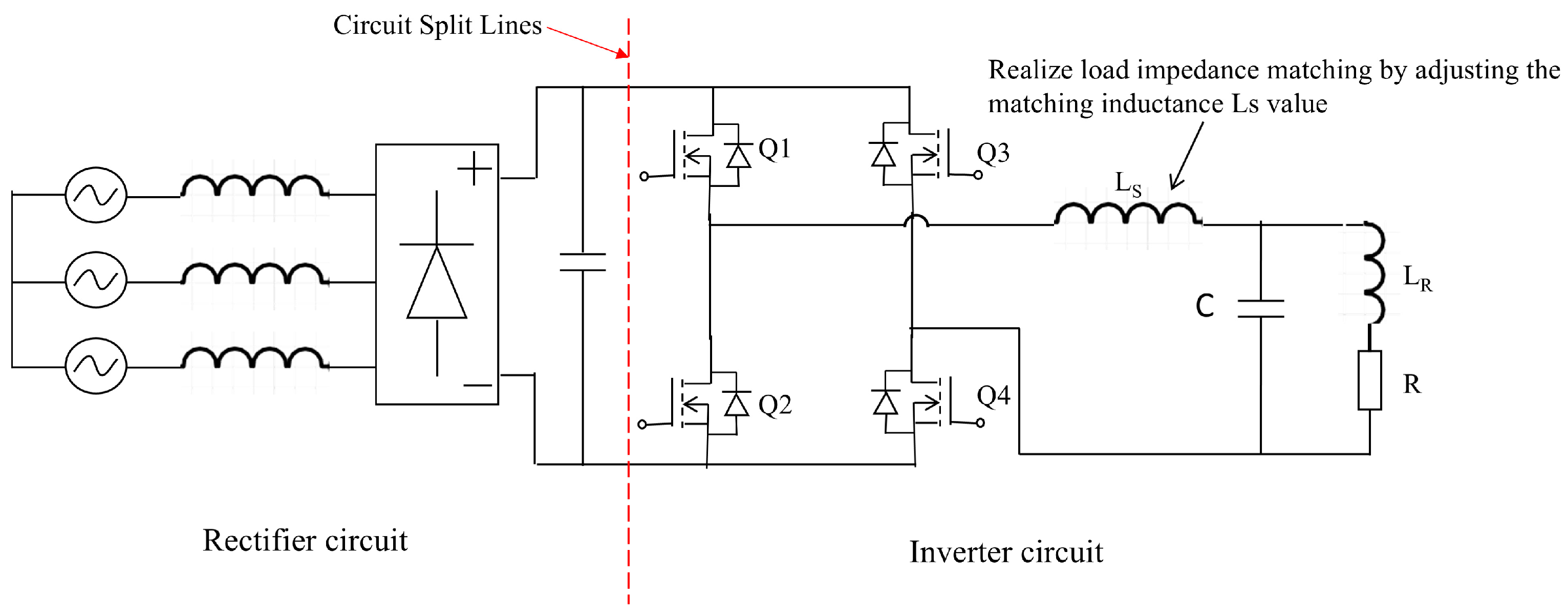
2.1. Principle of Full-Bridge LC Series Resonant Electromagnetic Induction Heating
Figure 1 shows the electromagnetic induction heating control system commonly used in industry, which consists of a rectifier circuit and an inverter circuit. The rectifier circuit converts the industrial-frequency alternating current (AC) into direct current (DC), and the inverter circuit adopts the circuit structure of full-bridge LLC series resonance, which realizes the inversion of voltage by controlling the two diagonal groups of the NMOS to turn on and off alternately. The inversion process refers to the process of transforming a DC voltage into an AC voltage at a certain frequency. However, a high current with a high frequency that passes through LS that usually needs a large-size in dimension and is not suitable for application in small induction heating devices powered by portable lithium batteries. In order to simplify the circuit, a simple full-bridge LC series resonant circuit structure is used in this paper, and the value of R in Figure 1 can be adjusted via the inverter frequency, thus achieving load impedance matching.
Figure 1.
Structure of full-bridge LLC series resonant circuit for industrial induction heating control system.
Figure 2a shows the structure of the miniaturized induction heating control system. Its structure is mainly divided into two parts: the DC side and the inverter side, where the DC side is the battery side, and the inverter side refers to the inverter circuit side with AC voltage output. UBAT represents the 3.7 V lithium battery supply voltage, and Q1 to Q4 are NMOSs controlled by four independent square-wave pulse signals from an MCU. Leq denotes the equivalent inductance of the inverter circuit, Req represents the equivalent resistance of the inverter circuit, and C is the resonant capacitor of the circuit. By controlling two diagonal groups of NMOSs, named Q1, Q4 and Q2, Q3, respectively, and alternately turning them on and off, the lithium battery’s output DC is converted into AC. The inverter frequency can be adjusted via the frequency control of the NMOSs to achieve load impedance matching.
Figure 2.
(a) The structure of the full-bridge LC series resonant circuit for a small induction heating control system. (b) The waveform when the UAB duty cycle is 50% and the power factor angle is φ.
Figure 2b shows a schematic diagram of the waveforms associated with the circuit. UAB is the inverter voltage between points A and B. UAB1 is the fundamental component of the inverter voltage, with a frequency equal to the inverter frequency, and determines the inverter current. IDC is the direct current from the battery and serves as a monitor of the circuit’s status. IAB is the sinusoidal current on the inverter side, and φ represents the phase difference, or power factor angle, between the inverter voltage and current.
In a full-bridge LC series resonant control system, the effective value of the fundamental component of the output voltage on the inverter side can be calculated:
where UDC is the output voltage of the battery UBAT.
The impedance of the inverter circuit is
where is the inverter angular frequency, and φ is the power factor angle of the resonant circuit.
The effective value of the inverter-side output current is
The inverter-side output power is
When the inverter-side frequency f equals the resonant frequency of the LC series circuit,
At this frequency, the power factor angle of the resonant circuit is 0, meaning that the inductive reactance and capacitive reactance cancel each other out, resulting in a minimum total impedance equal to the equivalent resistance Req. The current in the resonant circuit reaches its maximum value IAB0:
At this point, the voltage across the inductor coil and the resonant capacitor is
where Q is the quality factor of the resonant circuit, given by
According to Equation (8), at the resonant frequency f0, the voltages across the inductor and capacitor terminals are equal in magnitude but opposite in direction, thus canceling each other out. This ensures that the voltage across UAB1 is effectively applied across the equivalent resistance Req. At this frequency, the voltage across the inductor and capacitor terminals is Q times the root-mean-square value of the fundamental inverter-side voltage UAB1. The quality factor Q is an important parameter of the LC resonant circuit. A higher Q value indicates greater sensitivity of the circuit to frequency variations. In the design of heating systems, as the system transitions from the heating stage to the temperature-holding stage, the frequency gradually increases. During this transition, a high Q value effectively suppresses the increase in frequency, thereby reducing the NMOS losses of the transistor.
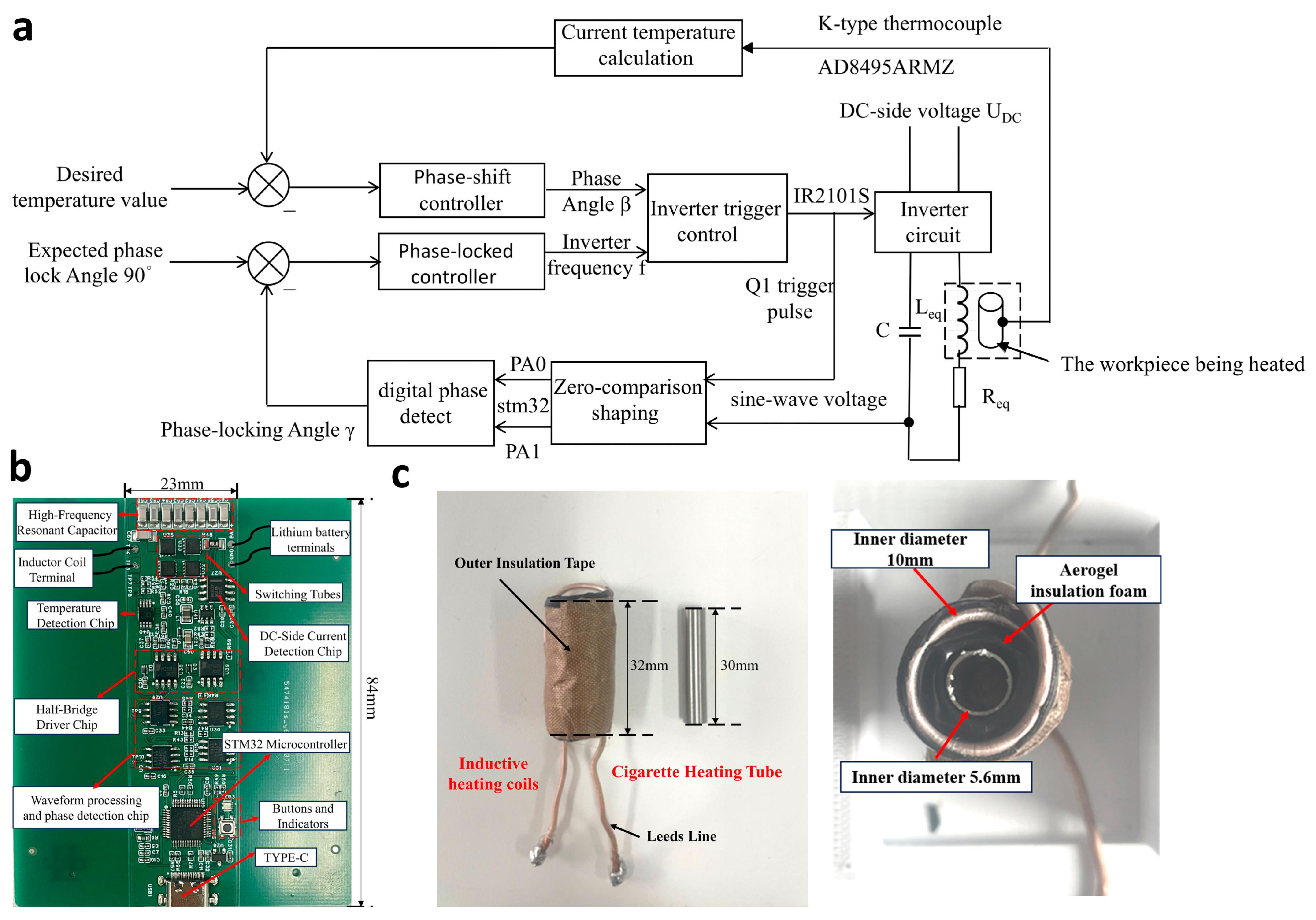
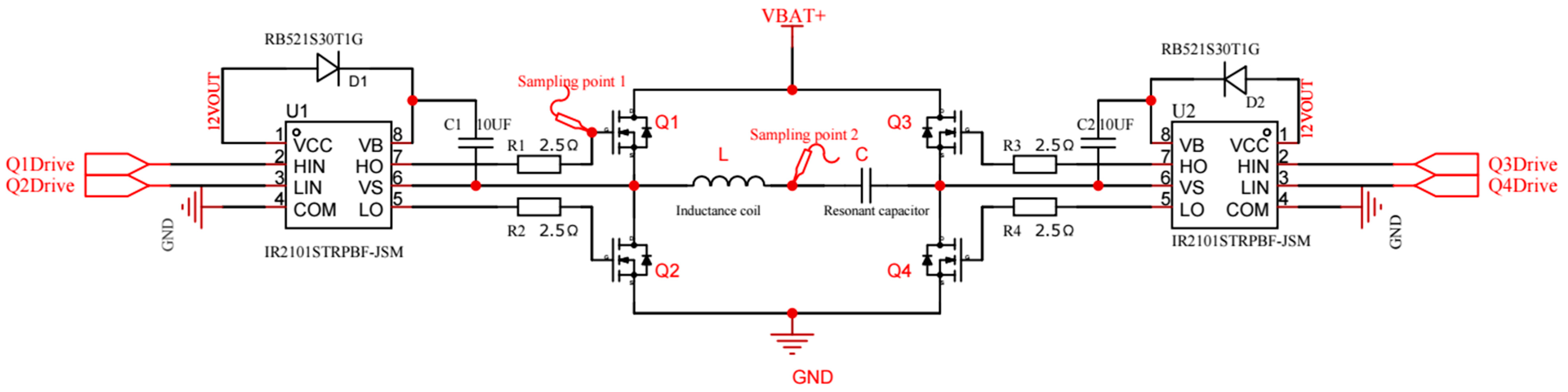
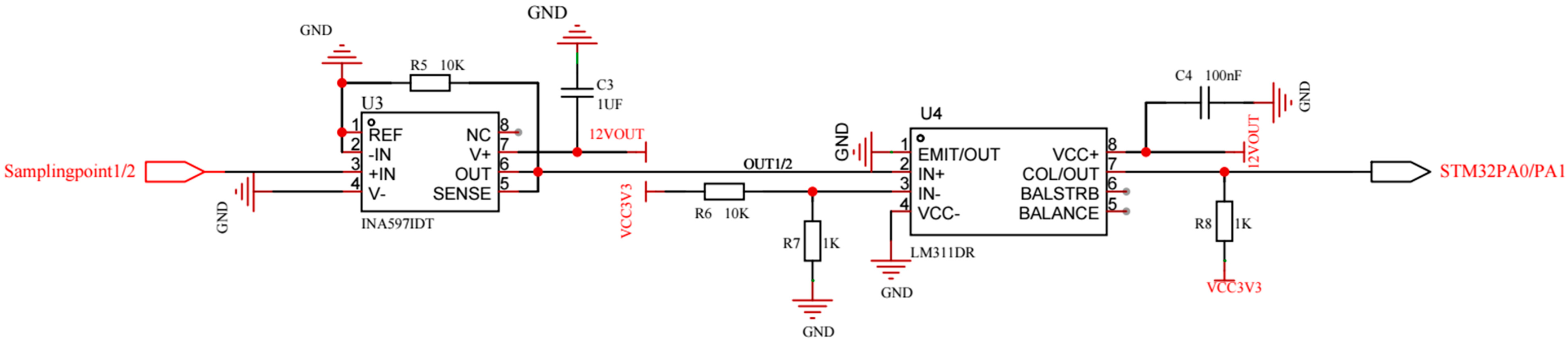
2.2. Low-Voltage-Powered Small-Size Electromagnetic Induction Heating Control System Structure and Circuit Principles
Figure 3a shows the overall structural framework of the small induction heating control system, and Figure 3b shows the layout of the PCB circuit board for the specific application of this structure in the design of heating non-combustible smokers. The PCB circuit board has a length of 84 mm and a width of 23 mm, and it is mainly divided into two modules: temperature control and frequency modulation (FM)-phase-locked control. The temperature control process requires power regulation, and power regulation requires FM-phase-locked control. Therefore, during the system operation, the two modules coordinate with each other to control the duty cycle and frequency of the NMOS drive signal, respectively. The NMOSs are controlled through the half-bridge driver chip IR2101S, into which the MCU signal is input.
Figure 3.
(a) Small electromagnetic induction heating control system’s overall structural frame. (b) Heating non-combustible vape control system’s PCB circuit boards. (c) Relative positions and dimensions of induction coils, heating tubes, and temperature-holding layers.
In the temperature control module, a K-type thermocouple and the AD8495ARMZ chip are used to collect temperature data from the heating tube. The difference between the collected current temperature and the target temperature is then input into a phase-shift controller to update the phase-shift angle β for the purpose of regulating the heating power for temperature adjustment.
In the FM-phase-locked loop module, to achieve the zero-current conduction of the NMOS, it is necessary to ensure that the rising edges of the drive pulses for Q1 and Q4 are aligned with the zero-crossing of the inverter current. Initially, square-wave pulse voltages for the Q1 drive and sinusoidal wave voltages from resonant capacitors are sampled and shaped through a zero-crossing comparison. They are eventually converted into two square-wave pulse signals with the same frequency but different phases. The MCU analyzes the phase difference between these two signals and adjusts the frequency through a phase-locked loop controller to achieve a phase difference of 90° between the two signals. This procedure eventually ensures the zero-current conduction of the NMOS.
In the temperature control process, the heating power is adjusted by the phase-shift angle β change, which will also cause variations in the phase difference between the Q1 drive pulse signal and the inner voltage of the resonant capacitor, and at this time, it is necessary to lock the phase difference by FM-phase locking. Therefore, in the control system work process, the temperature control module and the FM-phase-locking module can influence each other and must work in a coordinated and balanced state.
Figure 3c demonstrates the relative positions and dimensions of the inductor coil, heating tube, and temperature-holding layer. The inductor heating coil has an inner diameter of 10 mm and a length of 32 mm, and the heating tube has an inner diameter of 5.6 mm and a length of 30 mm. The inductor heating coil and the heating tube are filled with a temperature-holding aerogel to minimize the thermal conduction from the heating tube to the inductor coil.
Figure 4 illustrates the driving principle of the full-bridge NMOS configuration. The four NMOSs are controlled by two half-bridge driver chips, with Q1 and Q2 forming one pair and Q3 and Q4 forming the other pair. The input to the driver consists of two pulse-width-modulated (PWM) signals of the same frequency and complementary phase with dead-time intervals generated by the PWM function of the MCU. During system operation, when Q1 and Q4 are on, Q2 and Q3 are off. When Q2 and Q3 are on, Q1 and Q4 are off. Through the alternating on and off states of the two diagonal groups of NMOSs, the direction of the voltage at points A and B is continuously changed to realize voltage inversion. In this process, the direct control signal of the NMOS and the inverter voltage UAB have the same frequency, which is equal to the frequency of the MCU output signal. When the two diagonal NMOS drive pulses are the same, the duty cycle of the UAB voltage is 50%. When the drive pulses of these voltage pairs are phase-shifted, the duty cycle and RMS value of the UAB voltage are reduced. This allows the heating power to be regulated.
Figure 4.
The circuit diagram of the full-bridge NMOS driver for the small-size electromagnetic induction heating control system powered by a 3.7 V lithium battery.
Figure 5 shows the FM-phase-locked schematic diagram of the system. The INA597 and LM311 are used to process the Q1 drive voltage and the voltage signal on the inside of the resonant capacitor. The INA597 is used to derate the signals to bring the voltage down to within the allowable range of the LM311 input voltage, and the LM311 compares the signals over zero and finally transforms the waveform into a 3.3 V square-wave voltage. Then, two transformed pulse signals are input to the MCU for phase difference calculation, according to which the frequency is then adjusted and locked. Finally, the Q1, Q4 driving pulse is located at the zero-crossing point of the inverter current to realize the soft turn-on of the NMOS.
Figure 5.
The frequency phase-locked circuit diagram for the small-size electromagnetic induction heating control system powered by a 3.7 V lithium battery.
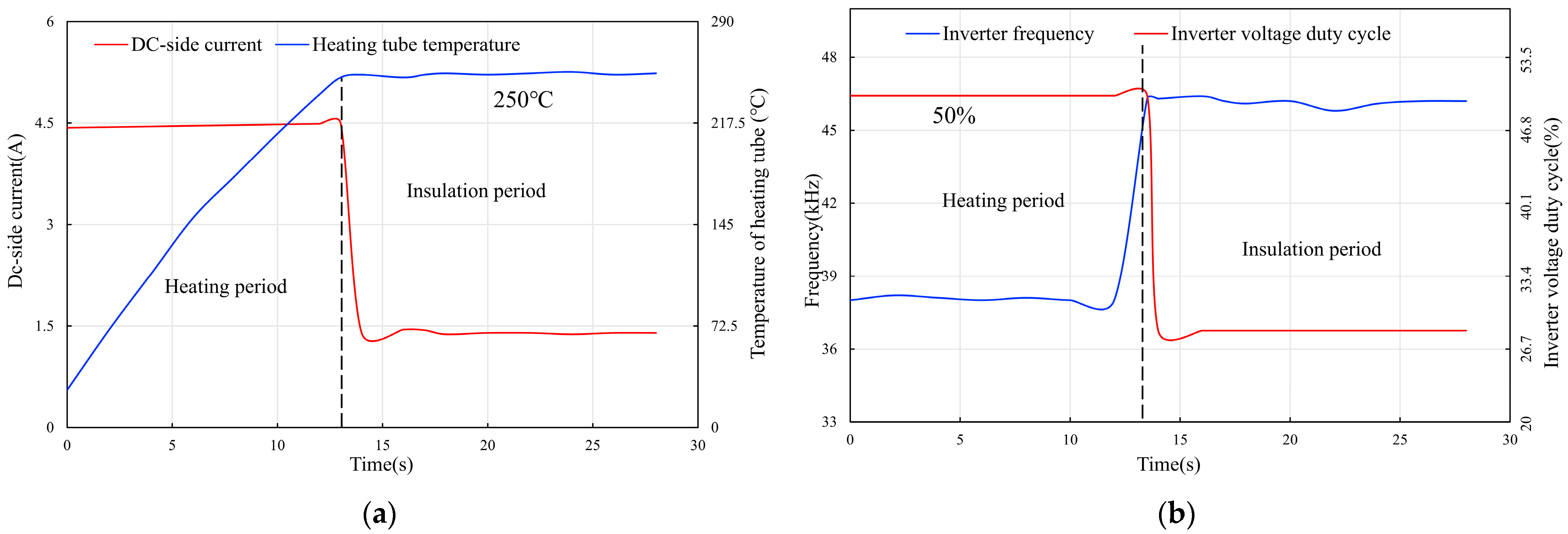
2.3. Electromagnetic Induction Heating Control System Work Process
This system employs a combined phase-shifting and frequency-locking power adjustment method. By adjusting the duty cycle of the driving pulse signals for Q1~Q4 to increase the phase-shift angle β, the value of UAB1 is changed. Simultaneously, the frequency-locking phase controller ensures that the rising edge of the driving pulse signals for Q1 and Q3 aligns with the zero-crossing point of the inverter circuit, thereby achieving soft switching. The STM32 timer can count cyclically between 0 and the auto-reload value (ARR). CCR is the value of the timer output comparison register. When the timer count value (INT) is greater than CCR, the timer outputs a low level, and when less than CCR, it outputs a high level. Therefore, the duty cycle of Q1, Q2 and Q3, Q4 can be adjusted by adjusting the value of CCR, and Q1, Q2 and Q3, Q4 are complementary pulses with complementary duty cycles. The variable X is set within a range of 0~1, and the CCR is adjusted by the variable X. Its relationship with the CCR of the two sets of pulse signals is as follows:
where CCR1 controls Q1, Q2 to drive the pulse duty cycle. CCR2 controls Q3, Q4 to drive the pulse duty cycle.
Figure 6 shows the driving pulses for Q1~Q4 during the system’s power adjustment process, as well as some important waveforms. UAB represents the square-wave voltage on the inverter side, with an amplitude equal to the lithium battery’s output voltage. When Q1 and Q4 are turned on while Q2 and Q3 are turned off, UAB is positive. Conversely, when Q2 and Q3 are turned on while Q1 and Q4 are turned off, it is negative. Thus, the inversion of voltage is achieved by controlling the on/off states of the diagonal pairs of NMOSs. The phase-shift angle β is the interval angle between the driving pulses for Q1 and Q3. When the phase-shift angle is β, the following applies:
Figure 6.
LC series resonant circuit operation process and NMOS drive pulses and related important waveforms during power adjustment process.
When the phase shift is β, by adjusting the frequency, the zero-crossing point of IAB is kept lagging behind the rising edge of the drive pulses for Q1 and Q3 by a very small phase-shift angle α. The purpose of this adjustment is to provide sufficient time for the NMOS commutation and to approximately achieve zero-current switching. Considering that the voltage across the capacitor always lags behind the current IAB by 90° in phase, this paper uses the voltage across the capacitor to phase-lock IAB with a phase-lock angle of 90°. By frequency modulation and phase locking, Q1 and Q3 can be maintained in a soft turn-on and high-current turn-off state during the power adjustment process, as shown on the right side of Figure 6.
Figure 7 describes the operation process of the heating non-combustion smoking device control system. It shows that the process can be divided into two periods: the heating and the temperature-holding period. During the heating period, when the inverter frequency equals the resonant frequency, the duty cycle of the drive pulses for Q1 to Q4 is 50%, at which point X = 0, β = 0, UAB1 is at its maximum, and the inverter current is also at its maximum. This state is used to heat the heating element, rapidly raising its temperature to 250 °C. At this time, all four NMOSs are in a soft-switching state, effectively avoiding large losses caused by high currents. When the system enters the temperature-holding period, the value of X increases, the phase-shift angle β increases, and the duty cycles of Q1 and Q3 decrease, while the duty cycles of Q2 and Q4 increase. With frequency modulation and phase-locked control, the inverter frequency continuously increases from the resonant frequency, causing the duty cycle of the inverter voltage to drop from 50% to about 28%. During this process, the DC-side current IDC gradually decreases until it stabilizes, and the temperature of the heating element ultimately stabilizes around 250 °C. In the heating period, both the turn-on and turn-off of Q1 to Q4 are in a soft-switching state. In the temperature-holding period, Q1 and Q3 are in a soft turn-on and high-current turn-off state. The NMOS losses also change in different periods.
Figure 7.
Under the initial conditions of an inductor coil wire diameter of 1.17 mm, a resonant capacitor of 2.2 uF, and a heating tube with a 0.1 mm wall thickness made of pure iron, variations in system parameters with the operation time are shown. (a) The variation in the DC-side current IDC and the temperature of the heating tube over time. (b) The variation in the inverter frequency f and the inverter voltage duty cycle D with time.
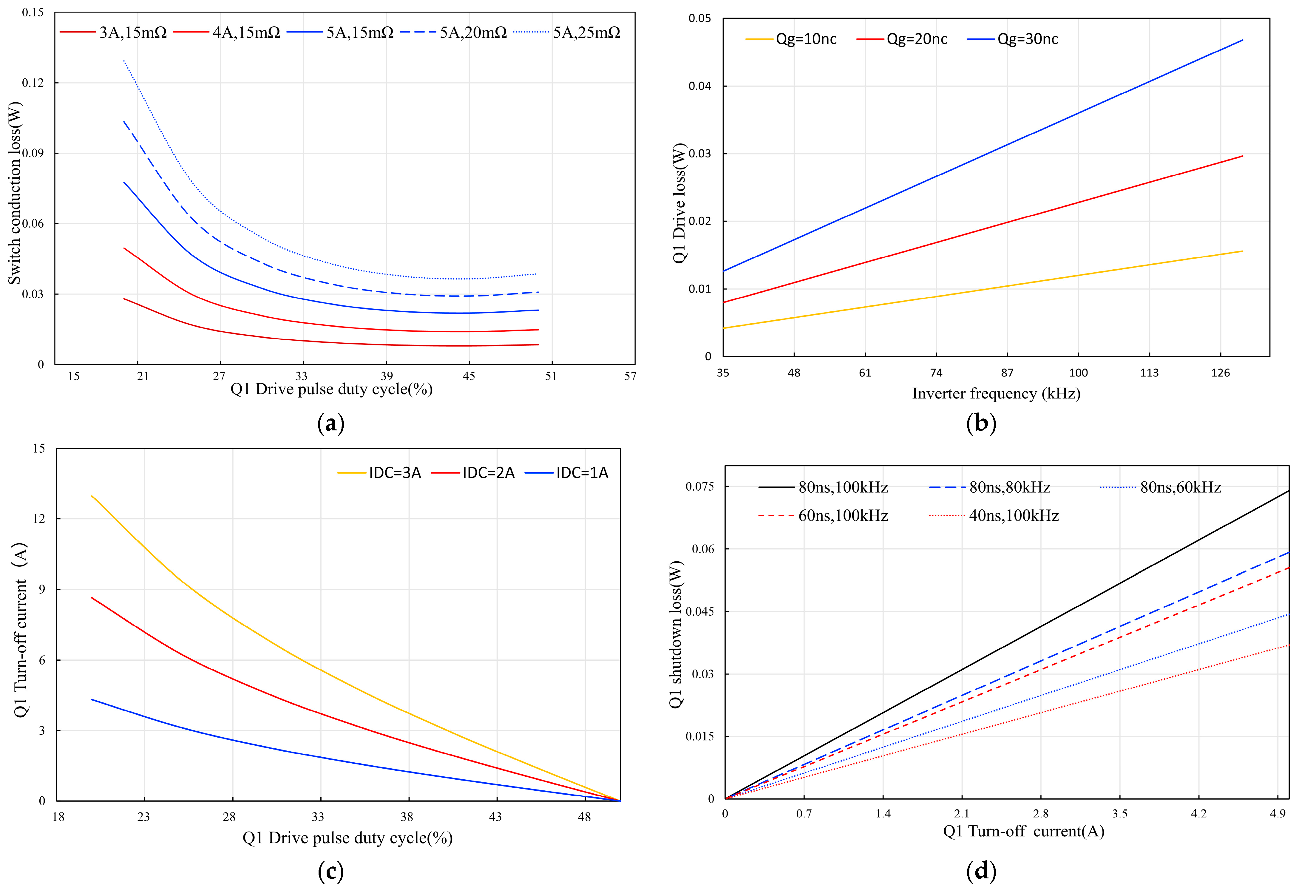
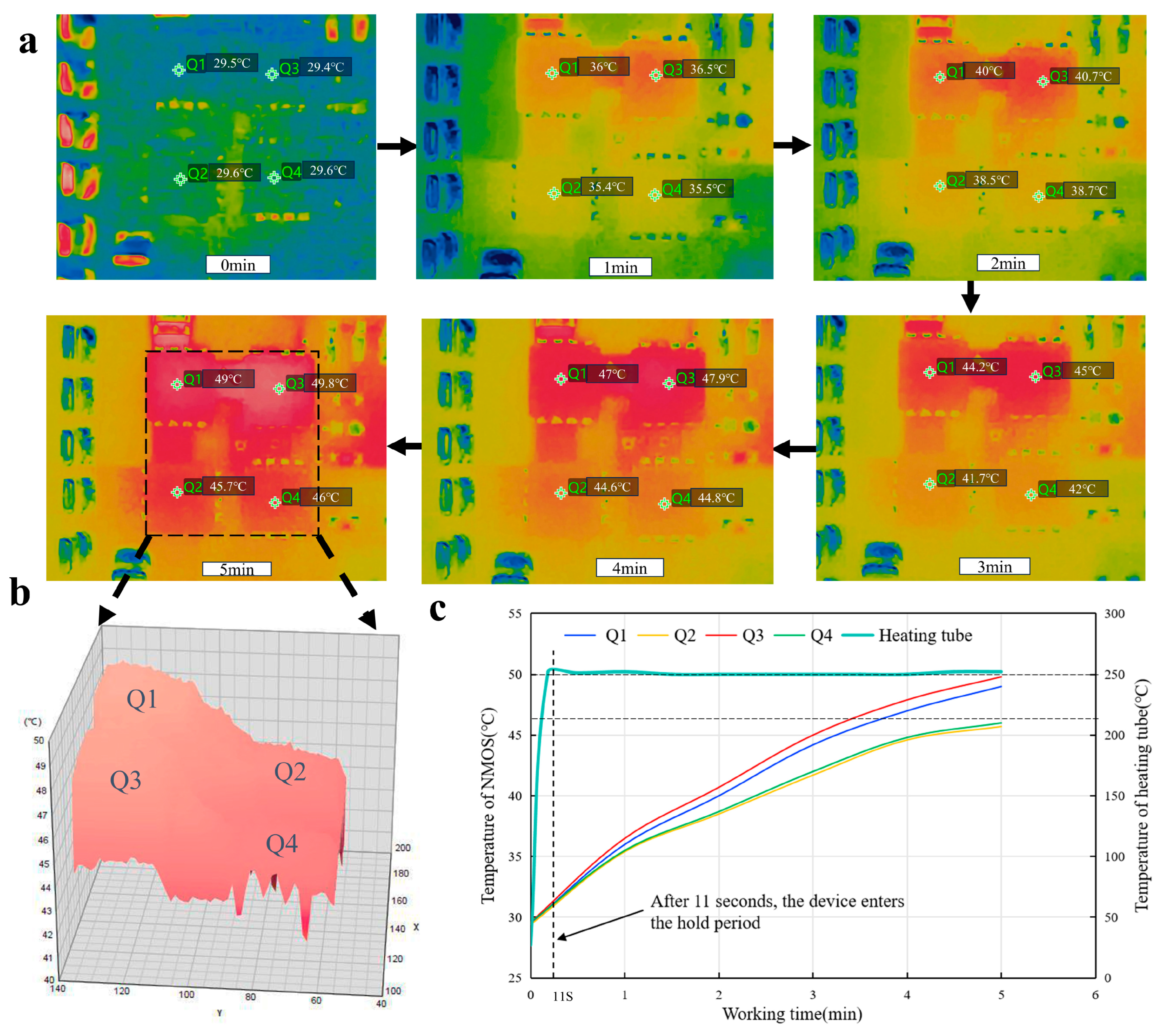
2.4. Impact Factor Analysis of NMOS Losses
The total loss of the NMOS in the small electromagnetic induction heating control system mainly consists of three parts: the conduction loss and driving loss of all NMOSs in the heating and temperature-holding period and the turn-off loss of NMOSs Q1 and Q3 in the temperature-holding period. In order to optimize the NMOS loss, the above three losses are calculated, and influencing factors are analyzed.
In the full-bridge LC series resonant circuit structure in Figure 2a, the output power on the DC side is approximately equal to the output power on the inverter side, so the following equation can be obtained:
The inverter current is
where
From the waveform relationship in Figure 8, we obtain
where β is the phase-shift angle, and D is the duty cycle of the drive pulses for Q1 and Q3.
Figure 8.
Figures showing the turn-off process of Q1. (a) The changes in the gate-to-source voltage VGS and gate drive current Ig during the turn-off process of Q1. (b) The variations in the drain-to-source voltage VDS and drain current IDS with time during the turn-off process of Q1.
Substituting the above into Equation (13) results in
At this time, the off-state current in the circuit is
where θ is the angle corresponding to the high level of the Q1 pulse.
From the circuit state relationship, the following is obtained:
Substituting the above into Equation (20) results in
From the analysis of Figure 8, it can be seen that the switching states of the diagonally opposite switches directly determine the direction and duty cycle of the inverter-side output voltage. Therefore, the diagonally opposite switches are grouped into pairs: Q1 and Q4 form one group, while Q2 and Q3 form another group. Since these two groups are symmetrical, only the loss analysis of Q1 and Q4 is required, where Q1 is the upper bridge arm, and Q4 is the lower bridge arm.
The conduction loss calculation formula for Q1 and Q4 is approximately
Substituting IAB from Equation (14) results in
where D is the duty cycle of the Q1 driving pulse. During the heating period, D = 0.5, at which time
The calculation formula for the driving loss of Q1 and Q4 is
where VDR is the NMOS’s driving voltage, f is the inverter-side frequency, and Qg is the total gate charge of the NMOS. During the heating and temperature-holding periods, the driving losses of Q1 and Q4 are the same.
From the above analysis, during the heating period, there are no turn-off losses for Q1 and Q4, while during the temperature-holding period, only Q1 introduces turn-off losses. Figure 8 shows the variations in parameters during the turn-off process. VDS is the NMOS drain–source voltage, IDS is the NMOS drain–source current, VGS is the NMOS gate–source voltage, VBAT is the battery supply voltage, and Ig is the NMOS gate drive current.
It is observed that the turn-off process mainly consists of two stages: t2 and t3. In stage t2, the IDS remains constant, and the VDS rises rapidly to VBAT. During this stage, the VDS and gate driving current remain unchanged, and the VDS is at the Miller plateau (a time period in which the VGS is held constant and the VDS voltage gradually rises or falls under the action of the Ig); the charge discharged in this stage is denoted by QGD. In stage t3, the VDS remains constant while the current drops quickly to zero. During this stage, the VDS drops to VGS(th), and the gate driving current decreases; the charge discharged in this stage is denoted by QGS2.
Based on the geometric relationship in Figure 8b, the Q1 turn-off loss during this stage is approximately
where f is the inverter-side frequency, and Uoff is the turn-off voltage, which is equal to the lithium battery supply voltage. Ioff is the turn-off current, which is calculated using Equation (21). toff is the turn-off loss time, consisting of two parts: t2 and t3, where
The total loss of Q1, Q4 during the heating period is
And, at this time, Q1, Q2, Q3, and Q4 have the same loss of power
During the holding time, the total loss of Q1 and Q4 is
At this time, the losses of the upper bridge arm NMOSs, Q1 and Q3, are the same, and the losses of Q2 and Q4 are the same:
Figure 9a shows the trend of Q1’s conduction loss with varying inverter-side duty cycles under different DC-side currents IDC and its own on-resistance RDS(on). It is clear that the conduction loss decreases with the increase in the inverter voltage duty cycle, regardless of the conditions. Additionally, for a constant RDS(on), the loss increases with increasing IDC. For a constant IDC, the loss increases with increasing RDS(on), and Q4 exhibits the same variation pattern as Q1.
Figure 9.
The analysis of various loss factors for NMOSs Q1 and Q4. (a) The conduction loss of Q1 varies with the duty cycle of its driving voltage for different IDC and RDS(on). (b) The trend of the NMOS’s driving loss with increasing inverter frequency f under different gate total charges Qg. (c) The variation in Q1’s turn-off current with the driving voltage duty cycle for different IDC. (d) Q1’s turn-off loss changes with the turn-off current under different toff and f.
Figure 9b illustrates the trend of the driving loss of the NMOS with increasing inverter frequency f under different gate total charges Qg. It is found that its loss increases with an increase in the inverter frequency and increases with an increase in its own Qg.
Figure 9c shows the trend of Q1’s turn-off current as the inverter-side duty cycle changes under different DC-side currents IDC. It shows that for the same IDC, the higher the duty cycle, the lower the shutdown current. At the same duty cycle, a larger IDC corresponds to a larger turn-off current.
Figure 9d demonstrates the trend of Q1’s turn-off loss with varying turn-off currents under different turn-off times toff and inverter frequencies f. It can be seen that the turn-off loss increases as the turn-off current increases in any case. Furthermore, for a constant toff, the loss increases with increasing f. For a constant f, the turn-off loss increases with increasing toff.
The above analysis reveals that the conduction loss of the NMOS is mainly related to its own on-resistance RDS(on), the DC-side current IDC, and the inverter-side duty cycle D. The driving loss is primarily influenced by the inverter frequency f, the NMOS’s own parameters Qg, and the driving voltage VDRV. The turn-off loss is mainly associated with the turn-off time toff, the turn-off current Ioff, and the inverter frequency f, where the turn-off current is primarily determined by the DC-side current IDC and the inverter-side duty cycle D.
2.5. Factors Affecting Resistance and Inductance of Coils
Figure 10a shows the trend of the number of strands included in the Leeds wire and the DC resistance of the coil as the wire diameter increases. The DC resistance of the coil decreases gradually from 0.017 Ω to 0.005 Ω as the wire diameter increases from 1.17 mm to 1.75 mm. At the same time, the increase in the number of Leeds wire strands suppresses the skin effect and thus reduces the AC resistance of the coil. Therefore, at the same frequency and magnitude of the current through the coil, a larger wire diameter will effectively reduce the coil’s own losses.
Figure 10.
(a) Trends of the number of wire strands and coil DC resistance with increasing wire diameter. (b) The trend of the equivalent inductance of the coil with increasing wire diameter with no load as well as under various load conditions.
Figure 10b shows the trend of the equivalent inductance of the coil with an increasing wire diameter under the no-load condition as well as when loaded with pure iron, 1J50 soft magnetic alloy, and 430 stainless steel with wall thicknesses of 0.1 mm and 0.2 mm for each load condition. The inductance gradually decreases from 2.36 uH to 1.14 uH under the no-load condition when the wire diameter is increased from 1.17 mm to 1.75 mm. All of the loading conditions increase the equivalent inductance of the coils compared to no load. And, the inductance decreases with the increase in the wire diameter. When the wall thickness is 0.1 mm, the equivalent inductance corresponding to 1J50 soft magnetic alloy is the largest, 430 stainless steel is the second largest, and pure iron is the smallest for any wire diameter. When the wall thickness increases to 0.2 mm, compared with 0.1mm, the equivalent inductance of the coil under the three materials is changed, of which 430 stainless steel corresponds to a relatively large change in inductance. Therefore, changes in the wire diameter and load conditions have an important effect on the equivalent inductance of the coil.
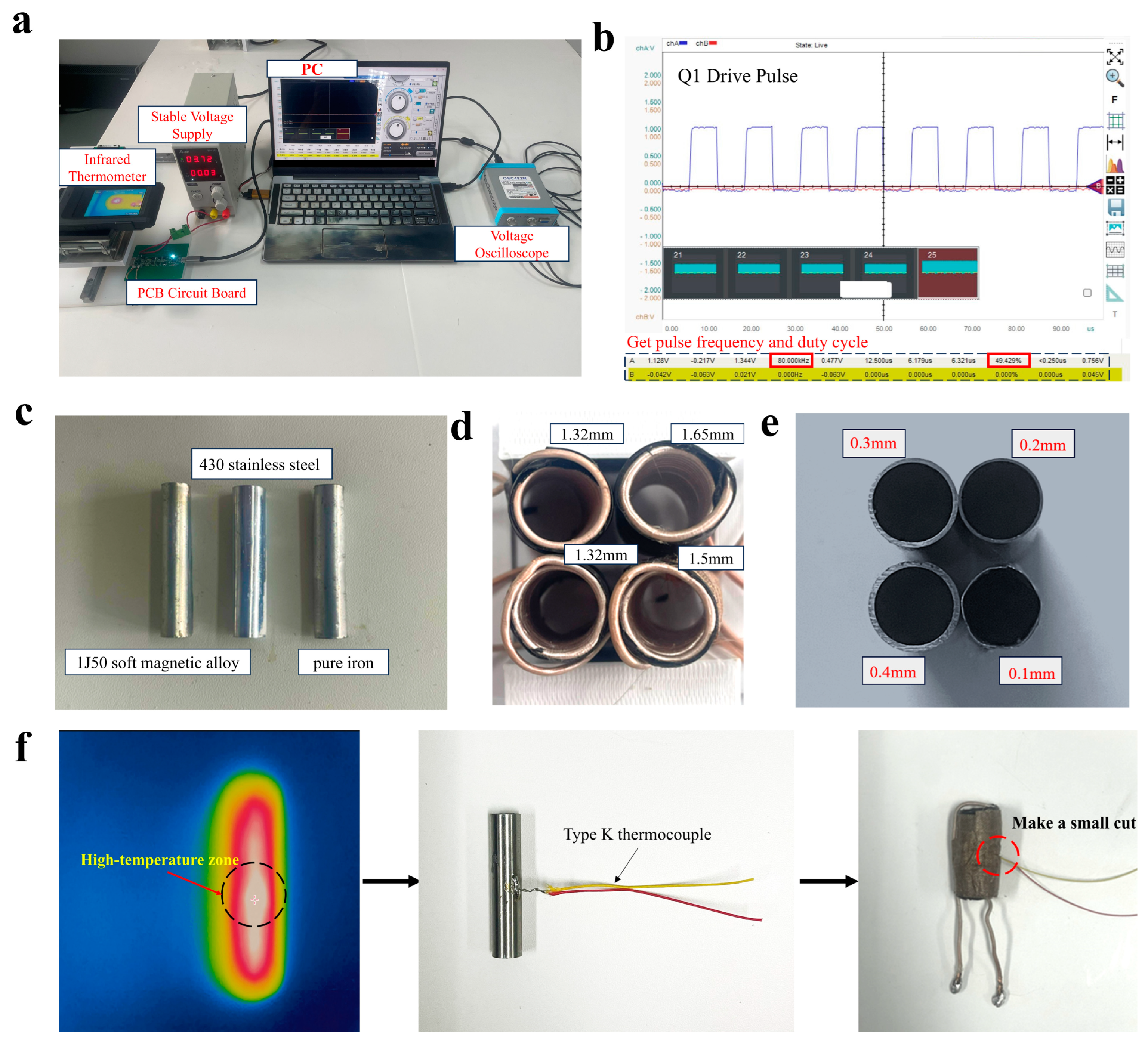
2.6. Experimental Setup
To improve the performance of the control system, the influence of the circuit parameters, including the resonant capacitance value, the wire diameter of the induction heating coil, the material, and the wall thickness of the heating tube, on the performance of the heating system was studied through experiments.
Experiments were conducted using a 1.17 mm induction coil wire diameter to explore the impact of capacitance changes on the heating rate of the tube and to calculate the NMOS total loss value at each stage simultaneously for the control system’s performance. To investigate the effect of different induction coil wire diameters, experimental tests were carried out on coils with five wire diameters of 1.17, 1.32, 1.5, 1.65, and 1.75 mm. The DC resistances of the induction heating coil at the above wire diameters were 0.017 Ω, 0.012 Ω, 0.0085 Ω, 0.006 Ω, and 0.005 Ω, and the inductance values under the no-load condition were 2.36 uH, 2.05 uH, 1.56 uH, 1.33 uH, and 1.14 uH, respectively. The heating rate of the heating tube was recorded at different capacitance values, and the NMOS total loss value was calculated at each stage. Three commonly used representative materials in induction heating, iron, 430 stainless steel, and 1J50 soft magnetic alloy, were selected for experimentation. Table 1 shows the physical parameters of the three materials. At the same time, in order to investigate the effect of the wall thickness on the performance of the control system, heating tubes with different wall thicknesses of 0.1, 0.2, 0.3, and 0.4 mm were employed to investigate the effect of wall thickness on the heating rate and the NMOS total loss.
Table 1.
Comparison of physical properties of three commonly used materials for induction heating.
Figure 11a displays the experimental setup for evaluating the performance of a small electromagnetic induction heating control system. A regulated power supply replaced the 3.7 V lithium battery to enable easier monitoring of the output current. Program commands were sent from a PC to the control system MCU and monitor the frequency and duty cycle of the oscilloscope’s output waveforms during the experiment. An infrared temperature meter measured the actual temperature rise of the NMOS. Figure 11c–e compare the appearance of the materials used, the wire diameter of the induction heating coil, and the wall thickness of the heating tube, respectively. Figure 11f illustrates the method used to measure the heating rate of the tube: an infrared temperature-measuring instrument observed the temperature distribution, revealing a ladder-like pattern with the highest temperature in the middle. To precisely control this peak temperature, a K-type thermocouple was positioned at the center of the heating tube. A small opening was cut in the middle of the induction heating coil to guide the thermocouple, preventing the temperature drift caused by the coil’s high frequency.
Figure 11.
The experimental setup. (a) The experimental platform for the performance testing of a small induction heating control system. (b) The output waveforms from the oscilloscope. (c) Three experimental materials: iron, 430 stainless steel, and 1J50 iron–nickel soft magnetic alloy. (d) Induction coil wires with different diameters. (e) The appearance of different wall thicknesses of heating tubes. (f) The temperature distribution of the heating tube and the arrangement of K-type thermocouples.
3. Results and Discussion
The correct NMOS parameter selection is crucial, as turn-off losses can significantly outweigh other losses. Therefore, minimizing turn-off losses is prioritized in NMOS selection, followed by reducing other losses. This paper employed the NCEP3065QU NMOS model (Wuxi New Clean Energy, Wuxi, China) as the inverter’s switching tube. Table 2 details the parameters for this NMOS model, showing a total of approximately 8 nC for QGD and QGS2 at a 12 V gate drive voltage, a Qg of around 30 nC, and an RDS(on) of just 1.9 mΩ.
Table 2.
N-channel MOS tube NCEP3065QU parameter details.
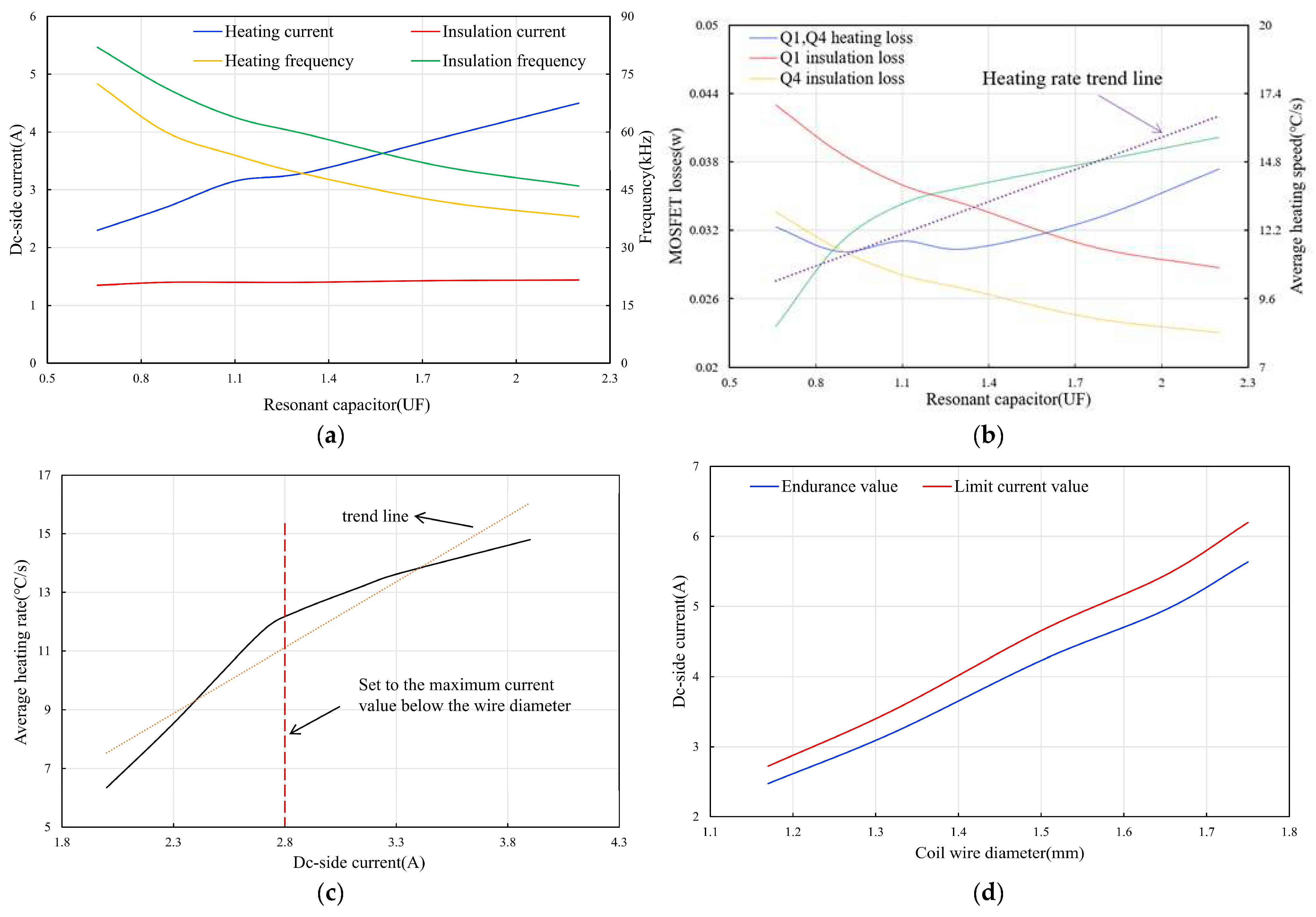
3.1. Effect of Resonant Capacitance Value on Heating Rate and NMOS Loss
A pure ferrous heating tube with a 0.1 mm wall thickness and a 1.17 mm coil wire diameter was used to examine the effect of capacitance on the operating performance of the control system. Figure 12a illustrates the impact of increasing capacitance on the DC-side current and inverter frequency of the system during both the heating and temperature-holding periods. Figure 12b depicts the variation in the heating rate of the heating tube and the power losses of Q1 and Q4 during these periods as the capacitance increases (Q2 and Q3 show symmetrical losses). It shows that as the frequency decreases, both Q1 and Q4 exhibit a reduction in losses during the holding period. However, due to the increased current during heating, losses slightly increase in this phase. Since the temperature-holding period is significantly longer than the heating period, losses during holding play a major role in the NMOS temperature rise. Therefore, increasing the capacitance overall helps reduce NMOS temperature-rise losses. Additionally, increasing the capacitance initially enhances the heating rate of the heating tube. However, once the capacitance exceeds a certain value, further increases lead to diminishing returns in heating rate enhancement.
Figure 12.
Experimental results under initial circuit conditions with a coil wire diameter of 1.17 mm and a 0.1 mm thick pure iron heating tube. (a) The DC-side current IDC and inverter frequency f during the heating and temperature-holding periods as the capacitance increases. (b) NMOS Q1 and Q4 losses and the heating rate of the heating tube during the heating and temperature-holding periods as the capacitance increases. (c) The trend of the average heating rate of the heater with increasing DC-side current. (d) The current withstand and limit values of coils correspond to the DC-side current in relation to the coil wire diameter.
Figure 12c shows the relationship between the time required for the heating tube to reach 250° C and the corresponding average heating rate as the measured DC current increases. The average heating rate is given by
It shows that the heating rate of the heating tube increases as the current increases. However, when the inverter current exceeds 1.1 times the maximum current rating of the coil wire diameter, the increase in the heating rate of the heating tube significantly slows down. Therefore, this paper defines 1.1 times the current rating of the wire diameter as the maximum current value for that wire diameter.
This study initially experimented with an iron heating tube with a 1.17 mm coil wire diameter and a 0.1 mm wall thickness to investigate the impact of capacitance on circuit parameters. It was observed that increasing the capacitance of the resonant capacitor enhances the heating rate to a certain extent and effectively reduces NMOS tube losses during heat preservation. However, excessive capacitance can decrease battery efficiency, as shown in Figure 12a, where exceeding 0.88 uF leads to the current surpassing the coil wire diameter’s limit, causing rapid resistance and temperature rises and diminishing battery efficiency. Therefore, selecting an appropriate capacitance value that ensures the current remains below the wire diameter’s limit improves the NMOS efficiency, heating rate, and battery efficiency. Figure 12d illustrates the relationship between the DC-side current, current withstand value, limit current, and coil wire diameter.
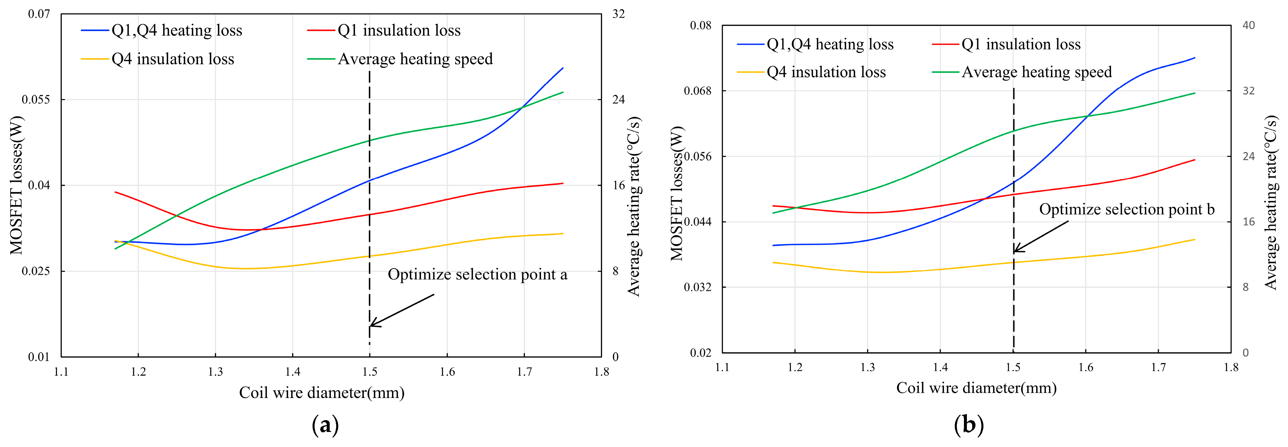
3.2. Effect of Induction Coil Wire Diameter on Heating Rate and NMOS Loss
Figure 13a–c illustrate the NMOS losses (Q1 and Q4) during the heating and temperature-holding periods and the heating rate of heating tubes (0.1 mm wall thickness)across different wire diameters for pure iron, 1J50 soft magnetic alloy, and 430 stainless steel. During heating, Q1 and Q4 losses increase consistently. In the holding period, losses for pure iron initially decrease and then rise while remaining stable for the other materials until wire diameters exceed 1.4 mm, where they gradually increase. Increasing the wire diameter enhances the heating rate, but beyond 1.5 mm, the rate slows, likely due to nearing magnetic saturation. This diameter corresponds to a battery output of approximately 4.5 A; larger diameters decrease the battery efficiency and increase NMOS losses. To ensure a fair performance comparison at a constant battery output, a 1.5 mm wire diameter was used for the induction coil.

Figure 13.
The effects of the wire diameter on NMOS losses and heating rates in induction heating systems. (a) Losses of Q1 and Q4 and heating rate variation with wire diameter for a pure iron heating tube (0.1 mm wall thickness). (b) Losses of Q1 and Q4 and heating rate variation with the wire diameter for a 1J50 soft magnetic alloy heating tube (0.1 mm wall thickness). (c) Losses of Q1 and Q4 and heating rate variation with the wire diameter for a 430 stainless steel heating tube (0.1 mm wall thickness). (d) A comparison of the heating rate and losses of Q1 and Q4 at optimized conditions (points a, b, c).
Therefore, this paper selected a 1.5 mm induction heating wire diameter with a 0.1 mm wall thickness for pure iron, 1J50 soft magnetic alloy, and 430 stainless steel heating tubes. Capacitance values were adjusted to set the battery output current to 4.6 A, optimizing circuit conditions at points labeled a, b, and c. Figure 13d compares the heating tube rates and Q1, Q4 losses during holding periods at these points. The analysis shows that points b and c achieve significantly faster heating rates than point a, despite higher losses during holding. Specifically, with a constant battery output power, 1J50 soft magnetic alloy and 430 stainless steel heat faster but also experience greater NMOS losses.
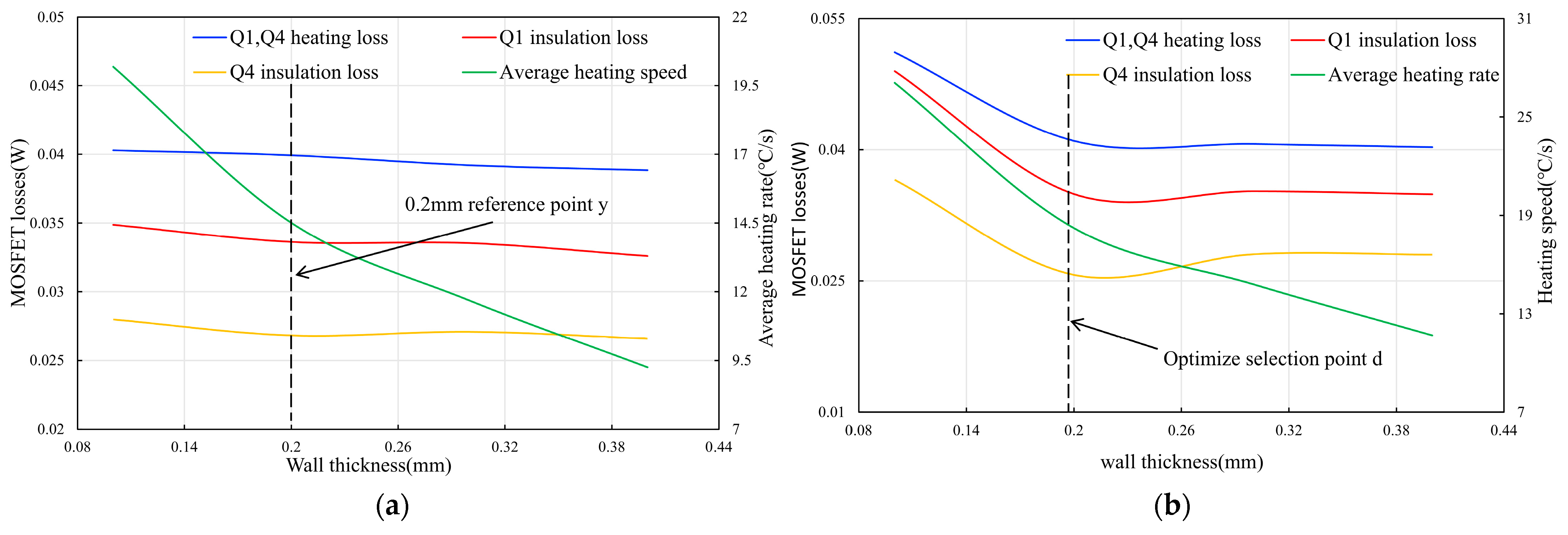
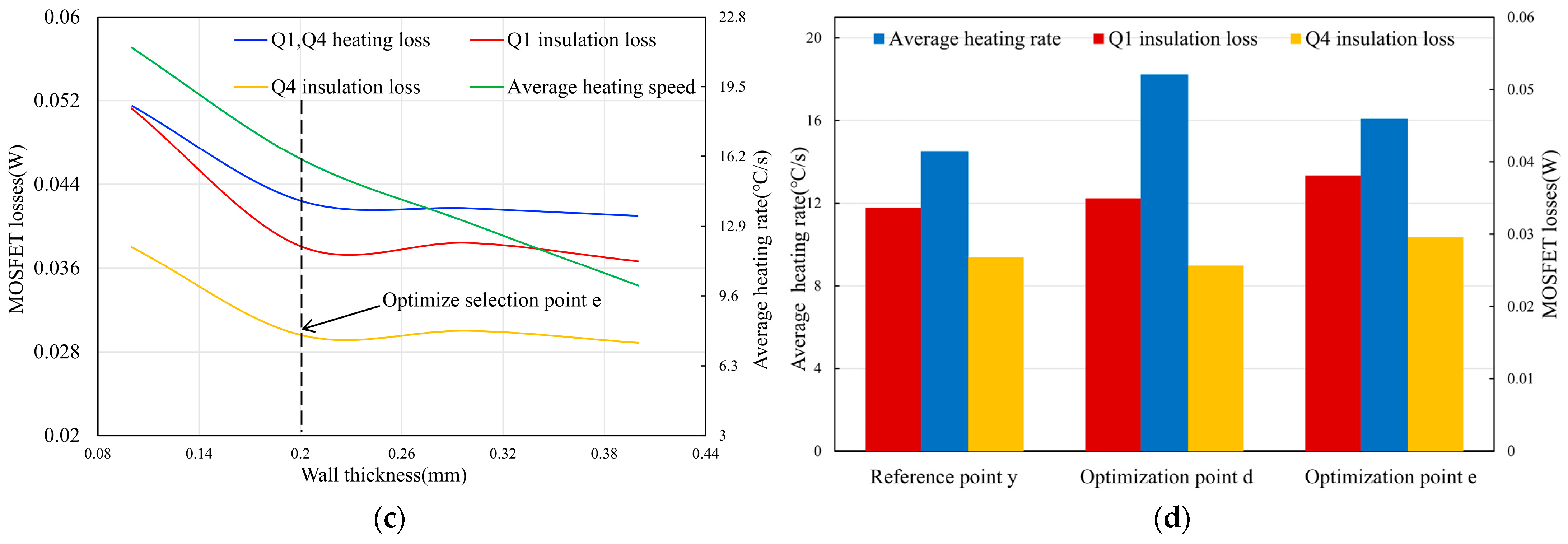
3.3. Effect of Heating Tube Wall Thickness on Heating Rate and NMOS Loss
Figure 14a, Figure 14b, and Figure 14c, respectively, show the variation in the heating rate with increasing wall thickness for heating tubes made of pure iron, 1J50 soft magnetic alloy, and 430 stainless steel, along with the corresponding NMOS losses (Q1 and Q4) during the heating and temperature-holding periods, under conditions of a 1.5 mm wire diameter and 4.6 A battery output current. It was observed that all three materials exhibited a noticeable decrease in the heating tube’s heating rate with increasing wall thickness, with slight reductions in Q1 and Q4 losses during the heating and temperature-holding periods.

Figure 14.
The impact of wall thickness on NMOS losses and heating rates in induction heating systems. (a) Changes in Q1 and Q4 losses and heating rate with increasing wall thickness for the pure iron heating tube. (b) Changes in Q1 and Q4 losses and the heating rate with increasing wall thickness for a 1J50 soft magnetic alloy heating tube. (c) Changes in Q1 and Q4 losses and the heating rate with increasing wall thickness for a 430 stainless steel heating tube. (d) A comparison of heating rate and Q1 and Q4 losses during the holding period at optimization points e, f, and g.
For iron heating tubes, Q1 and Q4 losses show minimal change with increased wall thickness. Therefore, a 0.1 mm wall thickness remains optimal for pure iron heating tubes due to faster heating rates. In contrast, 1J50 soft magnetic alloy and 430 stainless steel behave differently. When their wall thickness increases to 0.2 mm, Q1 and Q4 losses notably decrease, especially for 1J50 soft magnetic alloy. This is because, at a 0.1 mm thickness, both materials experience a continuous increase in the battery output current during heating, akin to nearing no-load conditions. Increasing the circuit’s inversion frequency to limit the current results in significantly higher NMOS losses compared to pure iron. A 0.2 mm wall thickness reduces this no-load effect. As the thickness further increases, the losses for these materials stabilize. Therefore, while the heating rate for 1J50 soft magnetic alloy and 430 stainless steel with a 0.2 mm thickness may not match that of 0.1 mm, the NMOS losses in the system are markedly improved.
Therefore, in this paper, using a 0.2 mm wall thickness and 1J50 soft magnetic alloy and 430 stainless steel as the heating tube materials, a 1.5 mm induction coil wire diameter was selected, and at the same time, the capacitance value was adjusted so that the output current of the battery reached 4.6 A so as to optimize the circuit conditions of point d and point e. Meanwhile, in order to compare the performance of the control system under the three materials with a 0.2 mm wall thickness, this paper also adjusted the output current of the battery to 4.6 A for the 0.2 mm wall thickness of the pure iron heating tube and optimized reference point y. Figure 13d demonstrates the heating rate of the heating tube under optimized points y, d, and e, as well as the trend of the losses of Q1 and Q4 in the temperature-holding period with the increase in wall thickness. By analyzing this figure, it is found that with a 0.2 mm wall thickness, the heating rate at points d and e is slowed down, but the loss is significantly reduced, especially at point d, which is approximately the same as that under the condition of the same wall thickness for a ferrous heating tube.
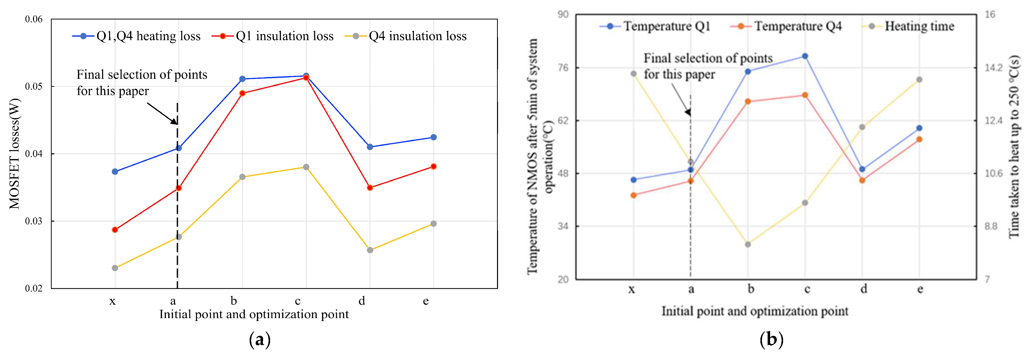
3.4. Comparison and Analysis of Initial Selection Point and Optimization Points
Under a consistent battery output current, the heating rate of the heating tube and the NMOS losses during both heating and holding periods were measured as benchmarks. Through comparison and analysis, five optimization points were selected. At these points, the control system’s induction coil wire diameter was set to 1.5 mm, with the battery current fixed at 4.6 A. To compare the control system’s performance with the initial setup using an iron heating tube with a 1.17 mm wire diameter and 0.1 mm wall thickness, adjustments were made to the heating tube material, wall thickness, and circuit resonant capacitance. This paper identifies these adjustments as optimization point x. Table 3 details specific circuit parameters across the five optimization points (a, b, c, d, e, x).
Table 3.
Comparison of circuit conditions for 6 selected optimization points.
Figure 15a compares the NMOS loss values at six selected points. Figure 15b contrasts the heating time required for the heating tubes and the temperature rise of NMOSs after 5 min of system operation at these points. The results reveal that the temperature rise at each point correlates closely with calculated loss values. Throughout, Q1 shows a higher temperature rise than Q4. Points b and c exhibit notably higher NMOS temperature rises, with Q1 exceeding 75 °C at point c. Point e falls in the middle, while points a and d show similar, relatively small temperature rises. Point x shows the smallest temperature rise. Regarding the heating time, point b requires the shortest duration, followed by points c, a, and d, while points x and e require the longest. It can be seen that points b and c have very fast heating rates but, at the same time, introduce a large NMOS temperature rise to the system, and point X has a small NMOS temperature rise, but due to the coil’s own loss, its battery efficiency is low and the heating time is long. Only point a has good performance in both the heating rate and NMOS temperature rise at the same time. Therefore, to improve the comprehensive performance of the control system, point a is selected as the best optimization point of this system, which has a faster heating rate and relatively small loss.
Figure 15.
A performance analysis of NMOS losses and heating dynamics in induction heating systems. (a) NMOS loss values (Q1, Q4) during heating and temperature holding at 6 optimization points. (b) The heating time and NMOS temperature rise (Q1, Q4) after 5 min of operation at 6 optimization points.
Figure 16a shows the infrared temperature distribution images of the NMOSs after running the device for 1 min, 2 min, 3 min, 4 min, and 5 min under the circuit conditions of optimization point a finally selected. Figure 15b depicts the 3D thermographic images of the four NMOSs after running the device for 5 min under the circuit condition of optimization point a. Analyzing this figure reveals that there is no significant difference in the temperature rises of the four NMOSs during the heating time period, but with the growth in the device operation time, the overall temperature rise of Q1, Q3 starts to be larger than that of Q2, Q4, and the temperature rise of Q2, Q4 is basically the same, while that of Q1, Q3 is slightly different due to the error in component parameters. Table 4 records in detail the performance of the control system’s operating performance under the circuit conditions at point a. Under a battery output current of 4.6 A, the temperatures of the upper bridge arm Q1 and Q3 are 49 °C and 49.8 °C, the temperature of the lower bridge arm Q2 and Q4 is about 46 °C, and the temperature of the outer layer of the coil is about 60 °C during the device running time of 5 min.
Figure 16.
The thermal analysis of NMOSs and the heating tube in the induction heating system. (a) Infrared temperature distribution of NMOSs after running the device for 1 min, 2 min, 3 min, 4 min, and 5 min, respectively. (b) A 3D thermogram of NMOSs after running the device for 5 min. (c) The trends of the NMOSs as well as the heating tube temperature with the device running time.
Table 4.
Optimal control system performance parameters.
4. Conclusions
This paper presents a small-size electromagnetic induction heating control system based on a full-bridge LC series resonant circuit powered by a 3.7 V lithium battery. By adjusting the resonant capacitor value, the system achieves load impedance matching. The paper focuses on design and optimization experiments for the application of this system in heating non-combustible smoking devices, aiming to address issues found in previous designs, such as slow heating rates, low battery efficiency, and large temperature rises in the switching devices. The optimal circuit conditions to meet the design requirements are found by taking the resonant circuit capacitance value, the wire diameter of the induction heating coil, the material, and the wall thickness of the heating tube as the optimization direction. The optimization results show that, compared with other circuit conditions, the selected parameters effectively improve the comprehensive performance of the control system. The system is able to heat the heating tube to the target temperature of 250 °C in 11 s at an output current of 4.6 A from the battery, and the temperature rise of all NMOSs is no more than 50 °C after the system runs for 5 min. In the future, the system circuit can be further optimized for functionality and structure to achieve lower energy consumption, higher heating efficiency, and reduced size. Additionally, the frequency-tracking control algorithm for inductive heating can be refined to enable faster and more accurate tracking of the electromagnetic induction resonant frequency. The proposed system can be used in medical, industrial, and a variety of personal portable heating equipment to achieve the safe, non-contact, high-efficiency heating or welding of small metal parts.
Author Contributions
Conceptualization, S.S. and Z.M.; Methodology, Y.L. and S.S.; Software, Y.L.; Validation, Y.L. and B.X.; Formal analysis, Y.L. and B.X.; Data curation, Z.L. and X.L.; Writing—original draft, Y.L.; Writing—review & editing, Z.L., X.L., Z.M. and J.L.; Supervision, Z.M. and J.L.; Funding acquisition, S.S. All authors have read and agreed to the published version of the manuscript.
Funding
This research received no external funding.
Data Availability Statement
The data are available from the corresponding author on reasonable request.
Conflicts of Interest
Authors declare that the research was conducted in the absence of any commercial or financial relationships that could be construed as a potential conflict of interest.
References
- Kukartsev, V.A.; Tynchenko, V.S.; Kukartsev, V.V. Steel smelting in induction crucible furnaces with industrial frequency. IOP Conf. Ser. Earth Environ. Sci. 2018, 194, 042024. [Google Scholar] [CrossRef]
- Phadungthin, R.; Haema, J. Full bridge resonant inverter for non-ferrous metal induction heating application. In Proceedings of the 2015 IEEE PES Asia-Pacific Power and Energy Engineering Conference (APPEEC), Brisbane, QLD, Australia, 15–18 November 2015; pp. 1–4. [Google Scholar]
- Phadungthin, R.; Haema, J. High frequency induction heating of full bridge resonant inverter application. In Proceedings of the 2016 International Symposium on Power Electronics, Electrical Drives, Automation and Motion (SPEEDAM), Capri, Italy, 22–24 June 2016; pp. 1383–1387. [Google Scholar]
- Smalcerz, A.; Wecki, B.; Blacha, L. Influence of the power of various types of induction furnaces on the shape of the metal bath surface. Adv. Sci. Technol. 2021, 15, 34–42. [Google Scholar] [CrossRef]
- El-Mashad, H.M.; Zhong, P. Application of induction heating in food processing and cooking. Food Eng. Rev. 2017, 9, 82–90. [Google Scholar] [CrossRef]
- Franco, C.; Acero, J.; Alonso, R.; Sagues, C. Inductive sensor for temperature measurement in induction heating applications. IEEE Sens. J. 2011, 12, 996–1003. [Google Scholar] [CrossRef]
- Meng, L.; Cheng, K.W.E.; Chan, K. Heating performance improvement and field study of the induction cooker. In Proceedings of the 2009 3rd International Conference on Power Electronics Systems and Applications (PESA), Hong Kong, China, 20–22 May 2009; pp. 1–5. [Google Scholar]
- Pijls, B.; Sanders, I.; Kuijper, E.; Nelissen, R. Segmental induction heating of orthopaedic metal implants. Bone Jt. Res. 2018, 7, 609–619. [Google Scholar] [CrossRef] [PubMed]
- Stauffer, P.R.; Cetas, T.C.; Jones, R.C. Magnetic induction heating of ferromagnetic implants for inducing localized hyperthermia in deep-seated tumors. IEEE Trans. Biomed. Eng. 1984, 31, 235–251. [Google Scholar] [CrossRef] [PubMed]
- Pijls, B.; Sanders, I.; Kuijper, E.; Nelissen, R. Non-contact electromagnetic induction heating for eradicating bacteria and yeasts on biomaterials and possible relevance to orthopaedic implant infections: In vitro findings. Bone Jt. Res. 2017, 6, 323–330. [Google Scholar] [CrossRef] [PubMed]
- Lucía, Ó.; Burdío, J.; Barragán, L.; Acero, J.; Millán, I. Series-resonant multiinverter for multiple induction heaters. IEEE Trans. Power Electron. 2010, 25, 2860–2868. [Google Scholar] [CrossRef]
- Park, H.P.; Jung, J.H. Load-adaptive modulation of a series-resonant inverter for all-metal induction heating applications. IEEE Trans. Ind. Electron. 2018, 65, 6983–6993. [Google Scholar] [CrossRef]
- Burdio, J.M.; Monterde, F.; Garcia, J.R.; Barragan, L.A.; Martinez, A. A two-output series-resonant inverter for induction-heating cooking appliances. IEEE Trans. Power Electron. 2005, 20, 815–822. [Google Scholar] [CrossRef]
- Bonert, R.; Lavers, J. Simple starting scheme for a parallel resonance inverter for induction heating. IEEE Trans. Power Electron. 1994, 9, 281–287. [Google Scholar] [CrossRef]
- Nam, I. Analysis and design method for parallel quasi resonant inverter in induction heating applications. In Proceedings of the 2018 IEEE Applied Power Electronics Conference and Exposition (APEC), San Antonio, TX, USA, 4–8 March 2018; pp. 1–5. [Google Scholar]
- Arslan, L.; Özbay, H. Modelling and simulation of D-class current-fed parallel resonant inverter for induction heating system. Aintelia Sci. Notes 2022, 1, 106–116. [Google Scholar]
- Kobos, W., Jr. Impedance matching of the inverter for induction heating. Relation 2018, 9, 1. [Google Scholar] [CrossRef]
- Esteve, V.; Jordán, J.; Dede, E.; Martinez, P.; Ferrara, K.; Bellido, J. Comparative analysis and improved design of LLC inverters for induction heating. IET Power Electron. 2023, 16, 1754–1764. [Google Scholar] [CrossRef]
- Esteve, V.; Jordán, J.; Dede, E.; Martinez, P.; Ferrara, K.; Bellido, J.L. Optimal LLC inverter design with SiC MOSFETs and phase shift control for induction heating applications. IEEE Trans. Ind. Electron. 2021, 69, 11100–11111. [Google Scholar] [CrossRef]
- Li, J.; Wang, L.; Sun, Q. Research on high-frequency induction heating load-matched based on LLC resonant circuit. In Proceedings of the 2014 International Power Electronics and Application Conference and Exposition, Shanghai, China, 5–9 November 2014; pp. 826–830. [Google Scholar]
- Kurre, M.; Banerjee, A. Zero voltage switching self-oscillating PWM inverter in induction heating applications. J. Eng. Res. 2022. [Google Scholar] [CrossRef]
- Yachiangkam, S.; Sangswang, A.; Naetiladdanon, S.; Koompai, C.; Koompai, C. Steady-state analysis of ZVS and NON-ZVS full-bridge inverters with asymmetrical control for induction heating applications. J. Power Electron. 2015, 15, 544–554. [Google Scholar] [CrossRef]
- Yongyuth, N.; Viriya, P.; Matsuse, K. Analysis of a full-bridge inverter for induction heating using asymmetrical phase-shift control under zvs and non-zvs operation. In Proceedings of the 2007 7th International Conference on Power Electronics and Drive Systems, Bangkok, Thailand, 27–30 November 2007; pp. 476–482. [Google Scholar]
- Kamli, M.; Yamamoto, S.; Abe, M. A 50–150 kHz half-bridge inverter for induction heating applications. IEEE Trans. Ind. Electron. 1996, 43, 163–172. [Google Scholar] [CrossRef]
- Lee, S.H.; Lim, S.; Song, S. Design of New Current Full-Bridge Resonant Inverter for Induction Heating System. J. Korean Inst. Illum. Electr. Install. Eng. 2012, 26, 59–69. [Google Scholar]
- Płatek, M.; Waradzyn, Z. Operation modes of full-bridge voltage-source series resonant inverter with PFM control for induction heating applications. Elektrotechnika Elektron. 2006, 25, 58–67. [Google Scholar]
- Lakkas, G. MOSFET power losses and how they affect power-supply efficiency. Analog. Appl. 2016, 10, 22–26. [Google Scholar]
- Kimball, J.W.; Chapman, P.L. Evaluating conduction loss of a parallel IGBT-MOSFET combination. In Proceedings of the Conference Record of the 2004 IEEE Industry Applications Conference, Seattle, WA, USA, 3–7 October 2004; pp. 22–26. [Google Scholar]
- Graovac, D.; Purschel, M.; Kiep, A. MOSFET power losses calculation using the data-sheet parameters. In Infineon Application Note; Infineon Technologies AG: Neubiberg, Germany, 2006; Volume 1. [Google Scholar]
- Esteve, V.; Jordan, J.; Sanchis, K.E.; Dede, E.J.; Maset, E.; Ejea, J.B.; Ejea, J. Enhanced pulse-density-modulated power control for high-frequency induction heating inverters. IEEE Trans. Ind. Electron. 2015, 62, 6905–6914. [Google Scholar] [CrossRef]
- Özbay, H. PDM-MPPT based solar powered induction heating system. Eng. Sci. Technol. 2020, 23, 1397–1414. [Google Scholar] [CrossRef]
- Yan, W.; Ji, Z.; Lu, X. Power control for induction heating by asymmetrical pulse density modulation. In Proceedings of the 2006 1ST IEEE Conference on Industrial Electronics and Applications, Singapore, 24–26 May 2006; pp. 1–5. [Google Scholar]
- Kumaraswamy, A.; Bhattacharya, A.; Sadhu, P. Dual output direct AC–AC series resonant converter for all metal induction heating system with a hybrid control technique. Electr. Eng. 2023, 105, 1363–1375. [Google Scholar] [CrossRef]
- Kwon, Y.S.; Lee, B.K.; Yoo, S.B. Half-Bridge Series Resonant Inverter for Induction Cooking Application with Load-Adaptive PFM Control Strategy. In ICPE (ISPE) Proceedings; Institute of Power Electronics: Seoul, Republic of Korea, 1998; Volume 10, pp. 1018–1023. [Google Scholar]
- Hu, J.; Bi, C.; Jia, K.; Xiang, Y. Power control of asymmetrical frequency modulation in a full-bridge series resonant inverter. IEEE Trans. Power Electron. 2015, 30, 7051–7059. [Google Scholar] [CrossRef]
- Zhou, M.; Li, Y.; Wang, J. Design of High Frequency Induction Heating Power Supply System. J. Harbin Univ. Sci. Technol. 2015, 20, 50. [Google Scholar]
- Jeong, W.; Heo, K.W.; Lee, J.S.; Jung, J.H. Phase-shifted third harmonic modulation technique for induction heating applications to improve soft switching capability. J. Power Electron. 2024, 24, 1014–1024. [Google Scholar] [CrossRef]
- Kifune, H.; Hatanaka, Y.; Nakaoka, M. Cost effective phase shifted pulse modulation soft switching high frequency inverter for induction heating applications. IEE Proc.-Electr. Power Appl. 2004, 151, 19–25. [Google Scholar] [CrossRef]
Disclaimer/Publisher’s Note: The statements, opinions and data contained in all publications are solely those of the individual author(s) and contributor(s) and not of MDPI and/or the editor(s). MDPI and/or the editor(s) disclaim responsibility for any injury to people or property resulting from any ideas, methods, instructions or products referred to in the content. |
© 2024 by the authors. Licensee MDPI, Basel, Switzerland. This article is an open access article distributed under the terms and conditions of the Creative Commons Attribution (CC BY) license (https://creativecommons.org/licenses/by/4.0/).