Abstract
This letter derives and discusses the superiority of a simple dc-link capacitor voltage control configuration for multilevel neutral-point-clamped converters with any number of levels. The control involves n − 2 control loops regulating the difference between the voltage of neighbor capacitors. These control loops are inherently decoupled, i.e., they are independent and the control action of one loop does not affect the others. This method is proven to be equivalent to previously published approaches, with the added advantages of increased simplicity and scalability to a higher number of levels, all while imposing a lower computational burden. The good performance of such control is confirmed through simulations and experiments.
1. Introduction
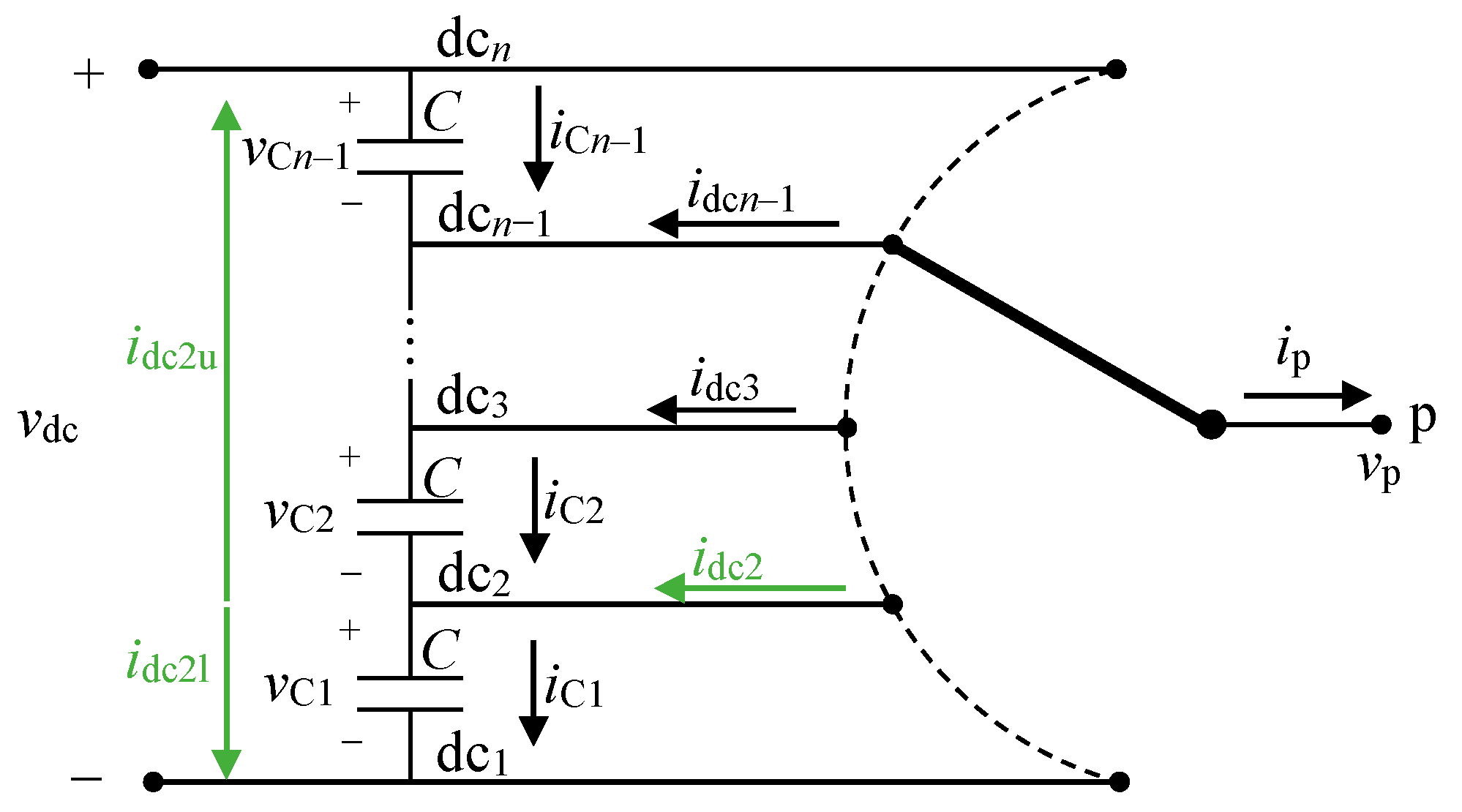
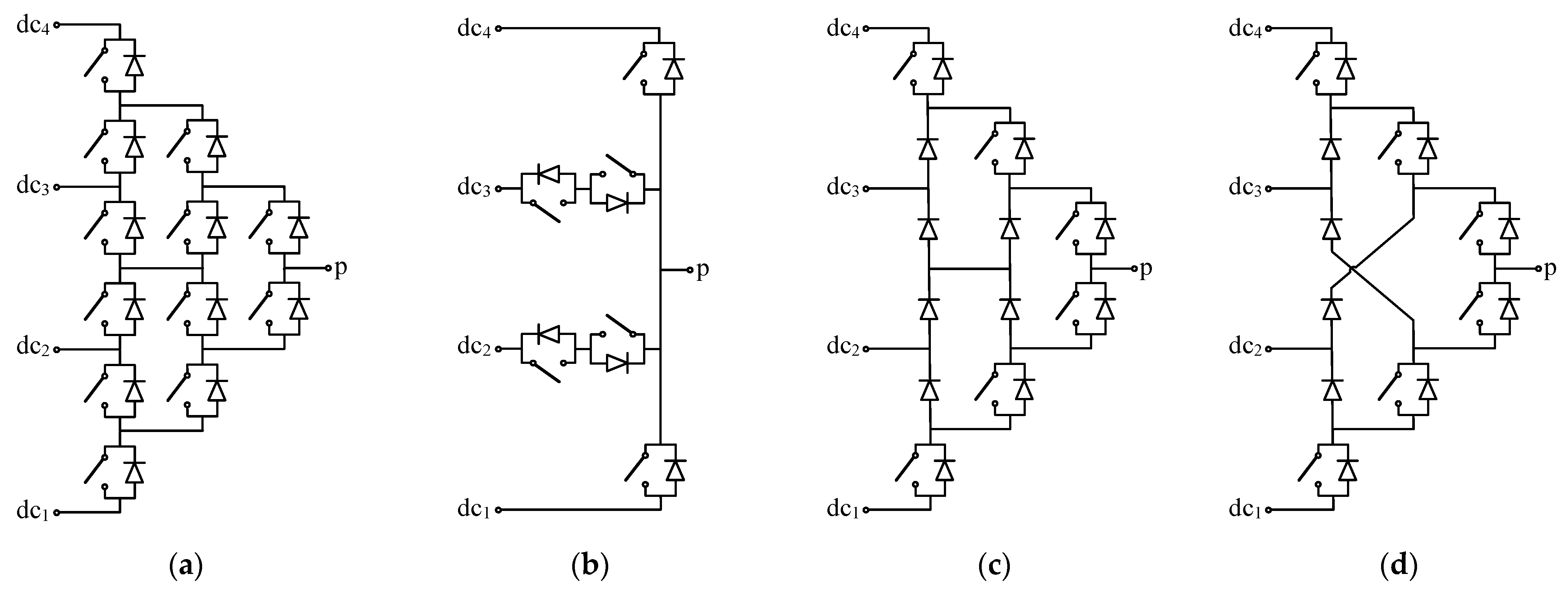
Multilevel conversion techniques are nowadays widely applied in power electronics systems, in a number of different applications and at low-, medium-, and high-power levels [1,2,3]. Among the multilevel topologies, the neutral-point-clamped (NPC) family stands as one of the most analyzed and applied, particularly at three levels. NPC conversion stages are configured by a set of converter legs connected to a common dc link, which is typically formed by a number of capacitors connected in series. Each converter leg, as depicted in Figure 1, behaves as a single-pole multiple-throw switch, connecting, at each point in time, the pole terminal p to one of the dc-link points: dc1 to dcn. These legs can be implemented through different circuit configurations [4]. Figure 2 shows some of them for the particular case of four levels. As can be observed, these legs only require a suitable combination of semiconductor devices with no capacitors or inductors, thus potentially featuring a very high power density.
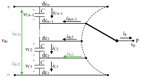
Figure 1.
Functional schematic of an n-level NPC converter leg.
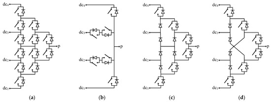
Figure 2.
Examples of four-level NPC leg topologies. (a) Transistor clamped. (b) Reduced transistor clamped or π-type. (c) Diode clamped. (d) Reduced diode clamped.
Each NPC converter leg receives as inputs the dc-link capacitor voltages vC1, vC2, …, vCn−1, forced by the capacitors, and the pole terminal current ip, forced by the external system connected to p. The NPC leg then imposes as outputs the pole terminal voltage vp and the dc-link currents idc1 to idcn. The inner dc-link or neutral-point currents, idc2 to idcn−1, are the ones responsible for the control of the dc-link capacitor voltage balance, a challenging and widely studied issue of NPC topologies [4]. Each average neutral-point current, as a result of the combined contribution of all converter legs, must be equal to zero (<idc2> = <idc3> = … = <idcn−1> = 0) to maintain a given capacitor voltage balance. Although challenging, suitable pulsewidth modulations have already been defined to meet this constraint for any number of levels, as explained in [4], which is a recent survey paper providing a comprehensive review of the literature in this field. However, converter nonidealities, such as mismatches in gate driving circuits, transistors or capacitors, and leakage currents, can still generate capacitor voltage imbalances that will need to be corrected through a proper closed-loop control, determining the suitable value of the neutral-point currents at each point in time. This letter derives and discusses the most beneficial approach to set up this control, i.e., the best option in the selection of the variables to be regulated, from the point of view of performance and simplicity. This method is proven to be equivalent to other possible variable selections if properly decoupled [5], with the added advantages of increased simplicity and scalability to a higher number of levels, all while imposing a lower computational burden.
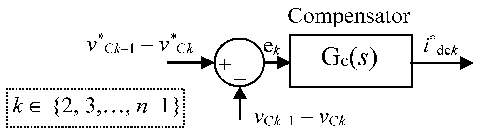
2. Inherently Decoupled Capacitor Voltage Balancing Control
Applying Kirchhoff’s current law and the characteristic equation of a capacitor, the neutral point currents can be expressed as:
with k ∈ {2, 3, n − 1}. From (1), it is clear that the voltage difference between neighbor capacitors can be controlled through the corresponding neutral point current. This leads to the control structure of Figure 3, with n − 2 control loops. These control loops, together with an additional converter control loop or external control of the total dc-link voltage vdc, enable the full control of all capacitor voltages to the commanded values.

Figure 3.
Proposed optimum control configuration for n levels.
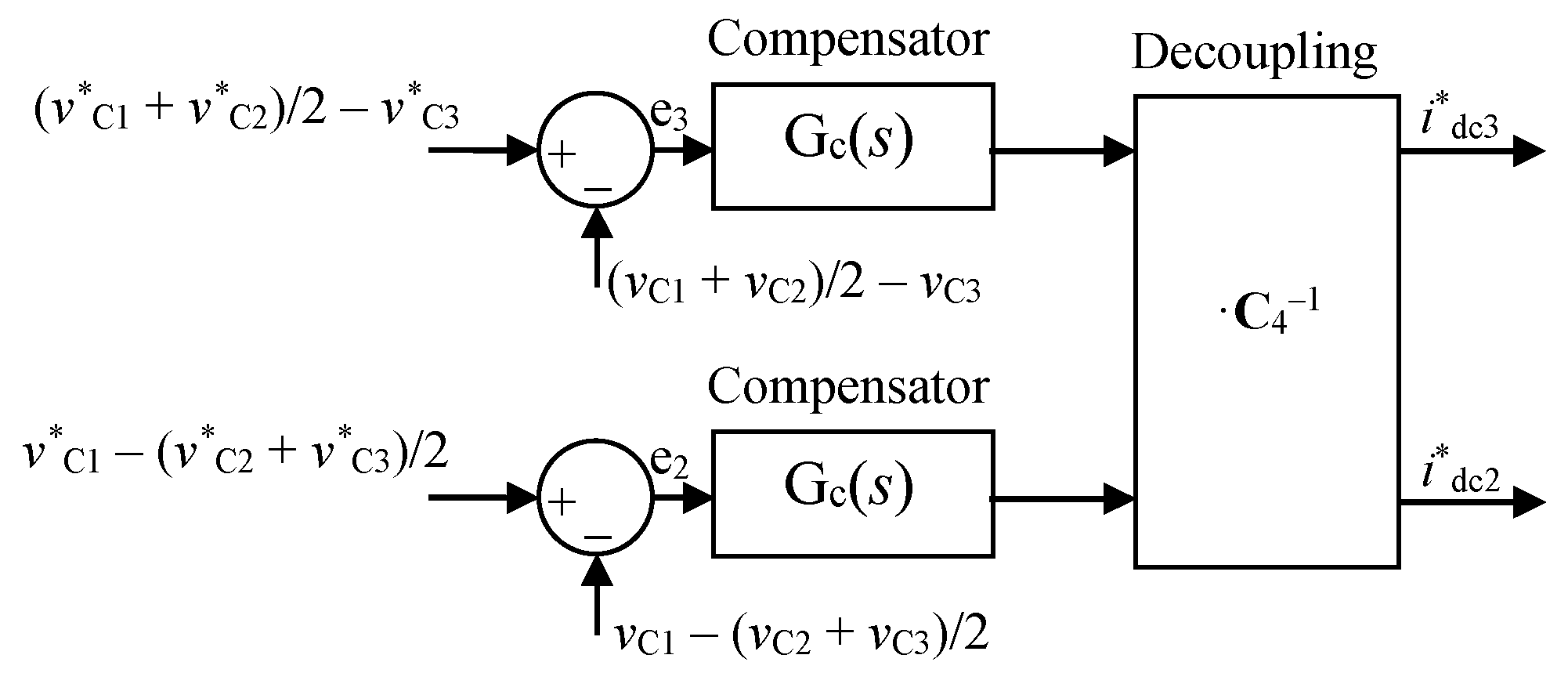
It is interesting to note that in this simple control structure, all control loops are inherently decoupled. Indeed, the value of idck only affects the value of vCk−1 − vCk. Current idck does not cause variations in the voltage difference between any other pair of neighbor capacitors. For instance, with reference to Figure 1, idc2 can be decomposed into two components: idc2u, which flows through the upper capacitors, C2, C3, …, and Cn−1, and idc2l, which flows through the lower capacitor C1. Assuming that all capacitors have equal capacitance, idc2u decreases vC2, …, vCk by the same amount, and idc2l increases vC1. Thus, overall, the injection of idc2 only affects the voltage difference vC1 − vC2 and does not vary the value of vCk−1 − vCk for k ≥ 3. In fact, the proposed control approach is completely equivalent to the control presented in [5] and illustrated in Figure 4 for four levels. In this control, the two loops are a priori coupled since
where
is the matrix of coupling coefficients. However, multiplying by the inverse of C4, as shown in Figure 4, the control becomes decoupled. Interestingly, if the decoupling matrix is directly applied to the regulated variables (the difference, at each neutral point, between the average bottom capacitor voltages and the average top capacitor voltages),
the new regulated variables of Figure 3 appear (the voltage difference between neighbor capacitors at each neutral point), which essentially proves that both control configurations lead to exactly the same behavior, while the control in Figure 3 is simpler. In fact, any alternative choice of the variables to be regulated in the control loops (individual capacitor voltages, neutral-point voltages, etc. [6,7,8,9,10]) leads to a coupled control system, where a decoupling would need to be applied for the best performance. Thus, the control configuration in Figure 3 is the most optimal, as it is the only one not requiring this decoupling.
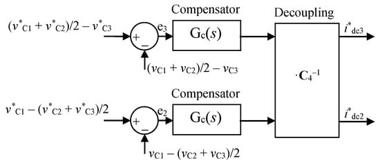
Figure 4.
Control configuration in [5] (four-level case).
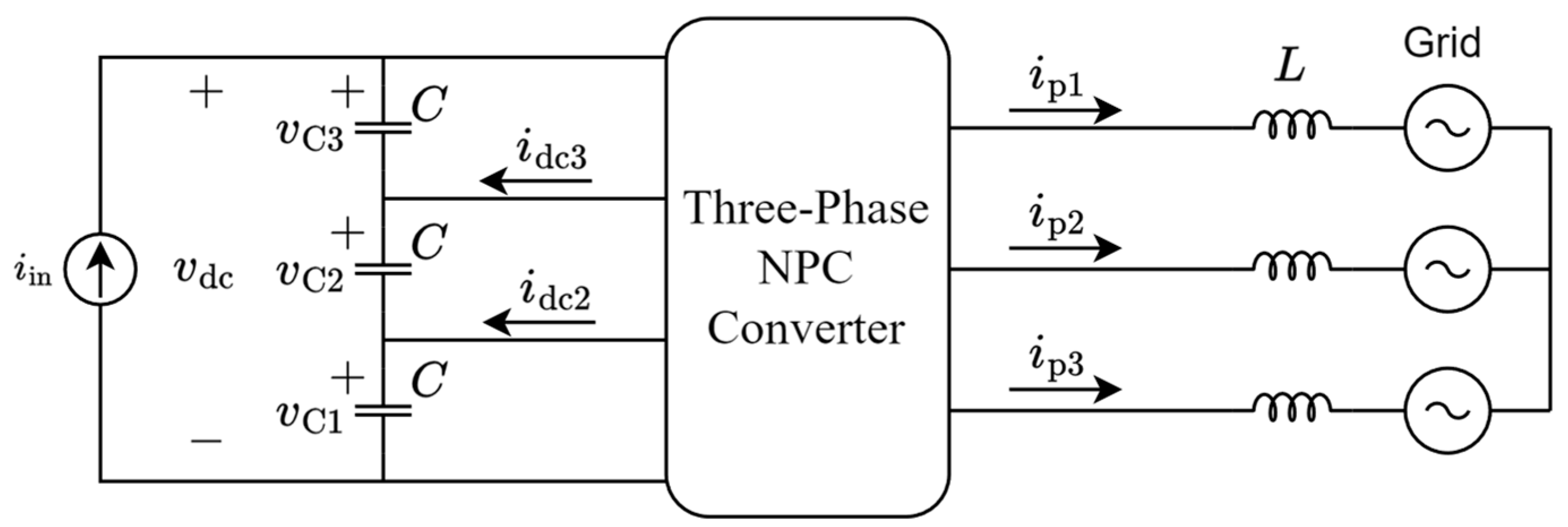
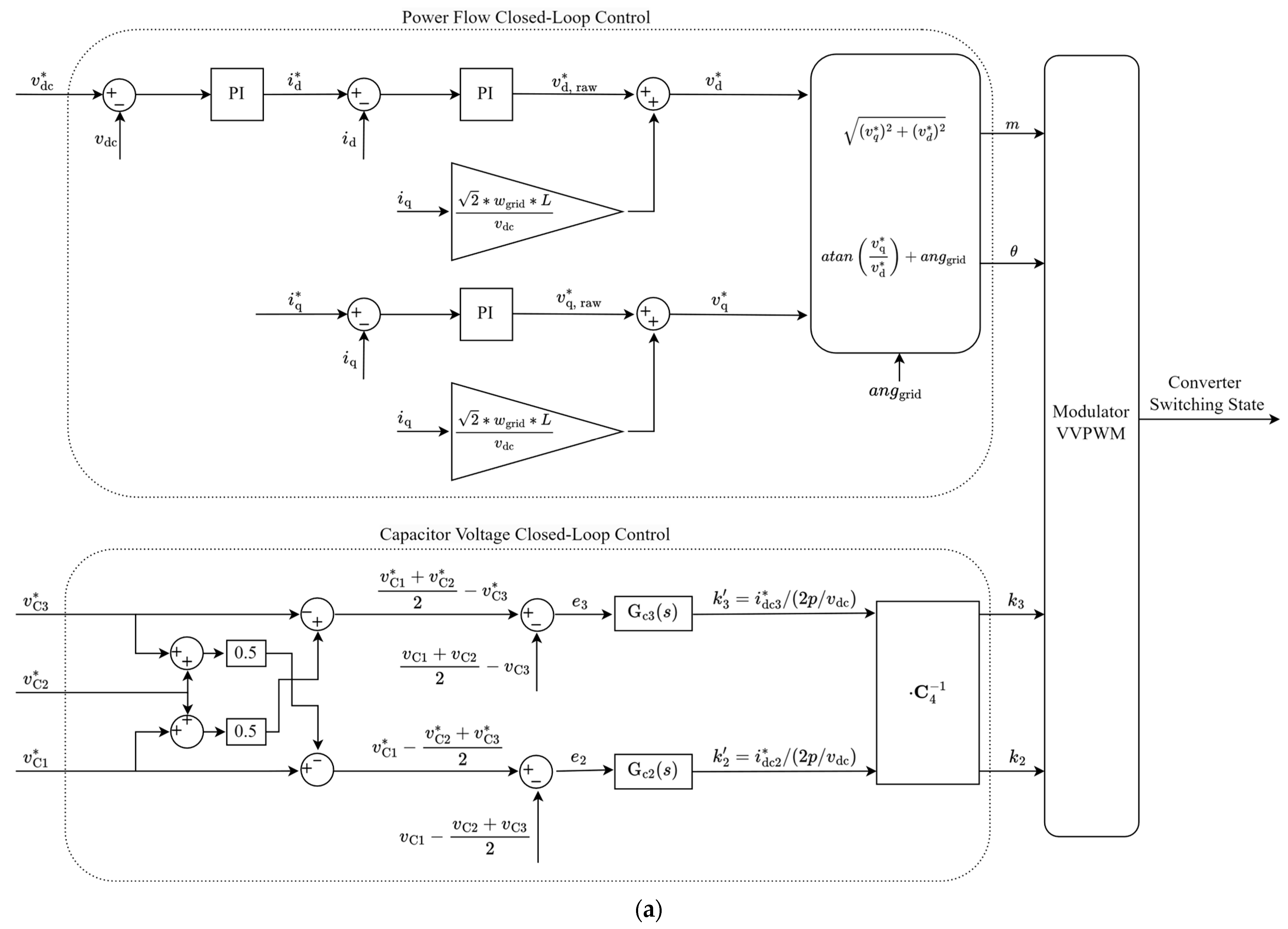
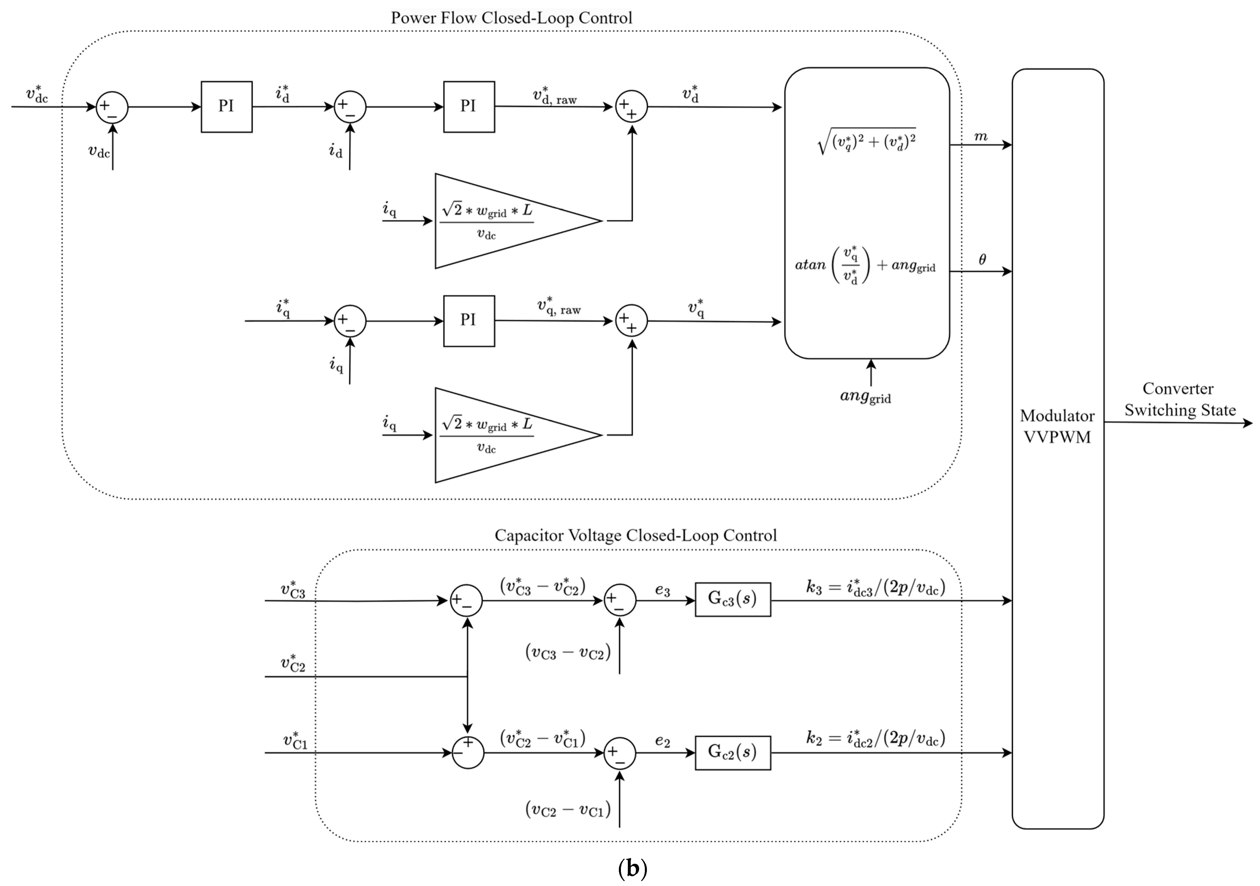
To better illustrate the proposed voltage balancing control in the context of a full system, a typical application is considered and depicted in Figure 5. A current source, representing a generic power source, is connected to the grid through a four-level, three-phase NPC inverter. A suitable control strategy to operate the system is presented in Figure 6. Two types of closed-loop controls are introduced. First, the closed-loop control is in charge of ensuring that all the energy supplied by the dc power source is transferred to the grid. This is achieved by regulating the dc-link voltage vdc = vC1 + vC2 + vC3. The error in the vdc is processed by a first PI compensator to produce the direct component of the grid current command, proportional to the active power to be transferred. An additional command of the in-quadrature component of the grid current is established, proportional to the desired reactive power. Two PI compensators then process the error in the direct and quadrature components of the current to finally generate the reference three-phase inverter output voltage vector in dq coordinates, vd* and vq*, which are finally converted into its polar coordinates: the modulation index, m, and the line-cycle angle, θ, both required by the modulator. A virtual vector pulsewidth modulation (VVPWM) with neutral-point current control, following [11], determines the converter switching state, establishing the connection of each NPC leg output ac terminal to a given dc-link point at each point in time. Second, the closed-loop control is in charge of regulating the dc-link capacitor voltages vC1, vC2, and vC3. The two loops in this control determine the values of the modulation parameters k2 and k3, which represent the normalized command value of the neutral point currents idc2 and idc3, respectively (p is the instantaneous power being transferred from the converter dc side to the converter ac side). In the case of the control loop presented in [5], corresponding to Figure 6a, more arithmetical operations are performed compared to the proposed simplified version shown in Figure 6b. In particular, the control loop in Figure 6a requires multiplying by the decoupling matrix C4−1.

Figure 5.
System diagram of a four-level, three-phase NPC grid inverter.
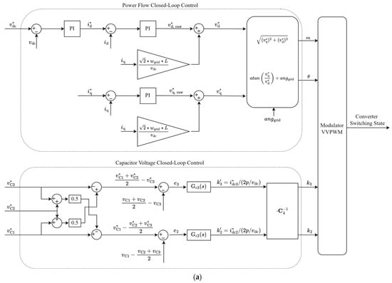

Figure 6.
Complete control block diagram of a four-level, three-phase grid inverter. (a) Decoupled structure following [5]. (b) Proposed simplified decoupled structure.
When the decoupled dc-link capacitor voltage control from [5] and the proposed control are implemented in Matlab, the proposed capacitor voltage control results in a reduction of the computation time of 45% for four levels and 65% for five levels. This performance improvement is due to the simplified definition of the control variables, which previously required multiple additions and products but now involves only a subtraction of two terms, as well as the elimination of the n − 2 by n − 2 decoupling matrix multiplication. Therefore, systems with a higher number of levels should benefit more from this optimization. At four levels, the new control strategy reduces the number of arithmetical operations of the decoupled control loop in [5] from 12 sums and 10 products to 4 sums and 2 products. At five levels, the arithmetical operations are further reduced from 27 sums and 20 products to 6 sums and 3 products.
While a few works in the literature have already proposed a control strategy involving the regulation of the difference of neighbor capacitor voltages (e.g., the work in [12]), the intended contribution of this paper is to reveal its inherent decoupling among control loops, its equivalence to the control proposed in [5], and to emphasize its superiority compared to other alternative options often applied in the literature. Table 1 presents a review of the most commonly used control variables, showing a significant diversity. The work presented in [6] defines the neutral-point voltages as the control objectives, leading to a rule-based control strategy where the larger absolute deviation takes priority. As a result, the selected redundant state minimizes only one neutral-point voltage error. Compared to the proposed approach, this control is strongly coupled and leads to poorer performance. These problems will increase as the number of levels increases. A different definition is used in reference [9], where the balance of the two outer capacitors of a four-level, three-phase converter is controlled by a zero-sequence voltage injection method, while the voltage of the inner capacitor is controlled by modifying the parameters of a redundant-level modulation. Two primary limitations restrict the feasibility of this solution. First, the control variables are coupled, leading to poorer voltage control. Second, the presented four-level, closed-loop control is not symmetric and scalable to systems with a higher number of levels. The approach in [10] is similar, where the balance of the two outer capacitors of a five-level converter is controlled by a zero-sequence voltage injection through a first control loop, while the other two control loops affect other modulation parameters. Similar to other solutions, in this approach, the control loops are coupled, multiple mathematical operations are required and it lacks scalability for higher number of levels. The different control variables used in these references are indicated in the second column of Table 1. All of the control variables present inherent coupling among control loops, defined by the corresponding coupling matrix. By multiplying the inverse of the coupling matrix by the control variables, the proposed variables in this letter arise.

Table 1.
Different definitions of control variables used in the literature.
In the case that the dc link is formed with battery modules in parallel with each dc-link capacitor, the regulated variable in each control loop (vCk−1 − vCk) should be replaced by the difference in the current of neighbor battery modules (iBk−1 − iBk) or their difference in state of charge (sck−1 − sck).
3. Simulation and Experimental Results
This section presents simulations and experiments that verify the good performance of the proposed inherently decoupled dc-link capacitor voltage control, in combination with a VVPWM [11] as in [5].
Simulations have been performed in Matlab-Simulink under different numbers of levels and phases. Figure 7 shows the schematic of the simulated system in the four-level, three-phase case. The dc link is fed by a constant voltage source, and a wye-connected multiphase series resistive-inductive load is assumed at the converter ac side with per-phase characteristic parameters R and L.
Figure 7.
System diagram of the three-phase, four-level NPC dc–ac converter employed in the simulations and in the experimental verification.
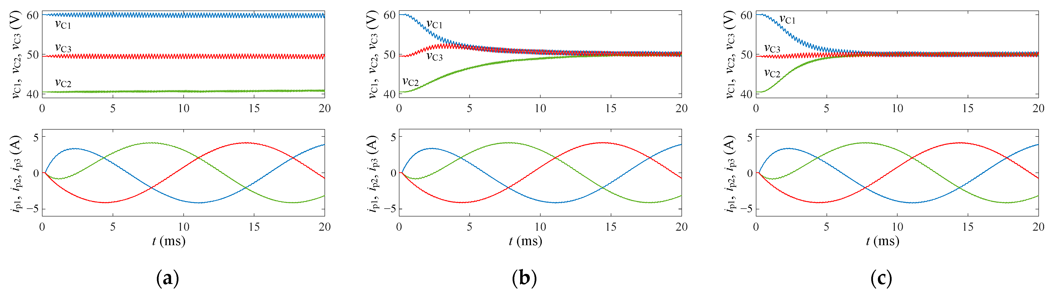
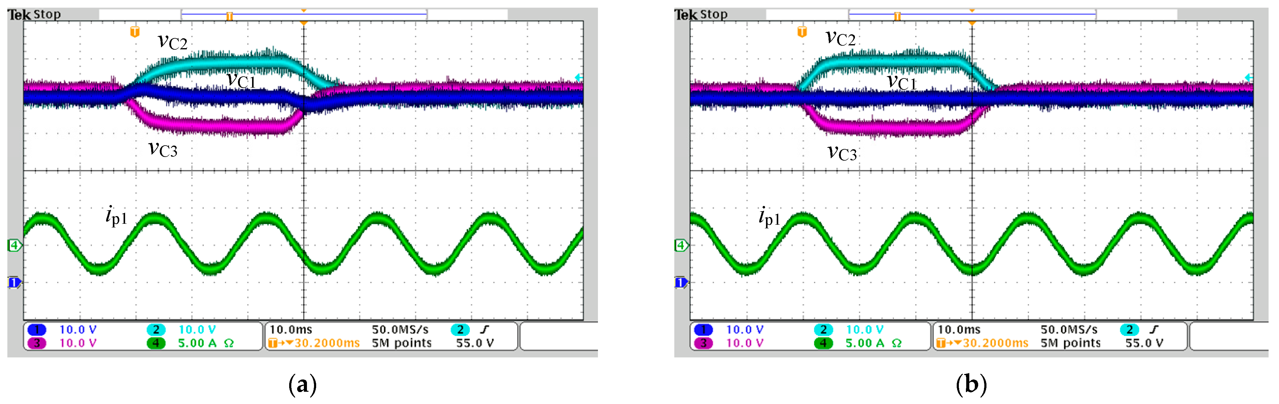
The first simulation, depicted in Figure 8, shows the system’s behavior under an initial voltage unbalance among the capacitor voltages in a four-level, three-phase system. When the control is not enabled, the initial voltages are maintained as the VVPWM modulation ensures zero average neutral point currents. Both the control from [5] without decoupling and the proposed inherently decoupled control are able to correct this initial deviation. It can be observed that the proposed decoupled control improves the transient response, especially in voltages vC3 and vC2. When the system is not decoupled (Figure 8b), vC3 shows an overshoot in the initial phase of the voltage correction, and the transient response of vC2 is considerably slower.
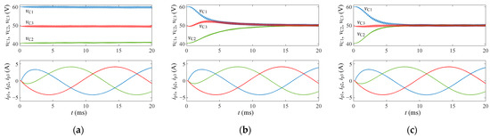
Figure 8.
Simulation results under unbalanced initial capacitor voltages of a four-level, three-phase system. Conditions: Vdc = 150 V, m = 0.5, C = 155 µF, R = 10 Ω, L = 10 mH, switching frequency fs = 5 kHz, and Gc(s) = 0.02/[1 + s/(1000π)]. (a) Control disabled. (b) Control in [5] without decoupling. (c) Proposed inherently decoupled control from Figure 3, which is exactly equivalent to the control in [5] with decoupling.
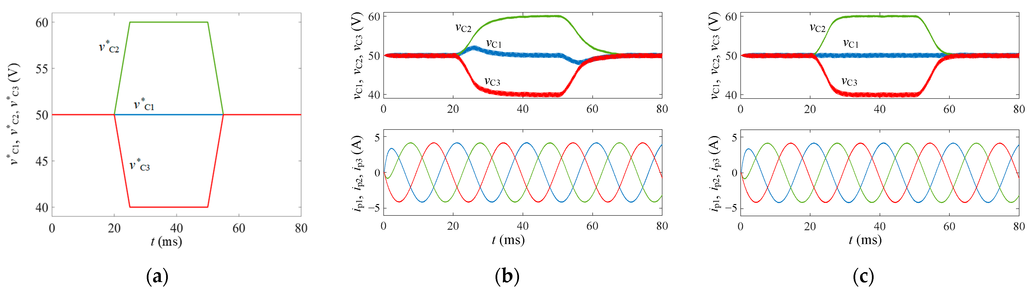
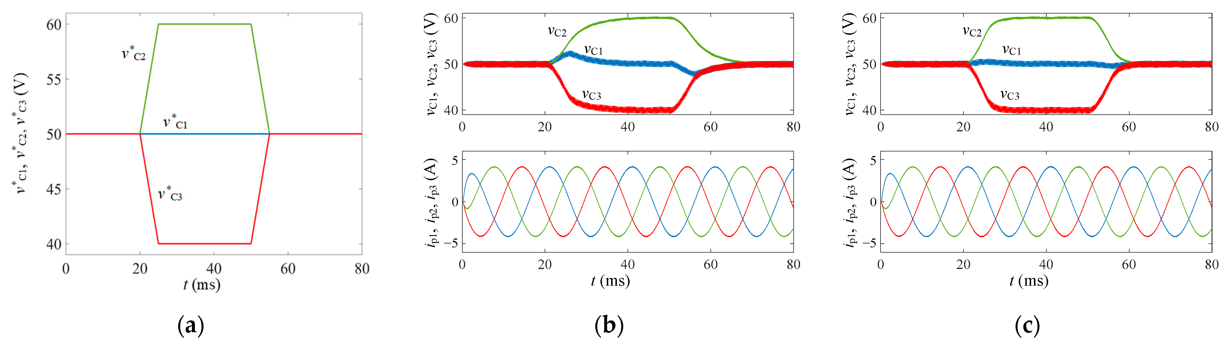
Figure 9 depicts the performance under ramp variations of v*C2 and v*C3 commands in a four-level, three-phase system. As it can be observed, under control in [5] without decoupling, undesired variations of vC1 occur, while these variations are fully suppressed with the proposed control.
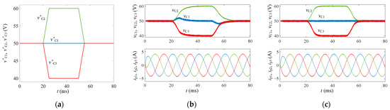
Figure 9.
Simulation results under ramp variations of the v*C2 and v*C3 commands of a four-level, three-phase system. Conditions: Vdc = 150 V, m = 0.5, C = 155 µF, R = 10 Ω, L = 10 mH, switching frequency fs = 5 kHz, and Gc(s) = 0.02/[1 + s/(1000π)]. (a) Capacitor voltage command values. (b) Control in [5] without decoupling. (c) Proposed inherently decoupled control from Figure 3, which is exactly equivalent to the control in [5] with decoupling.
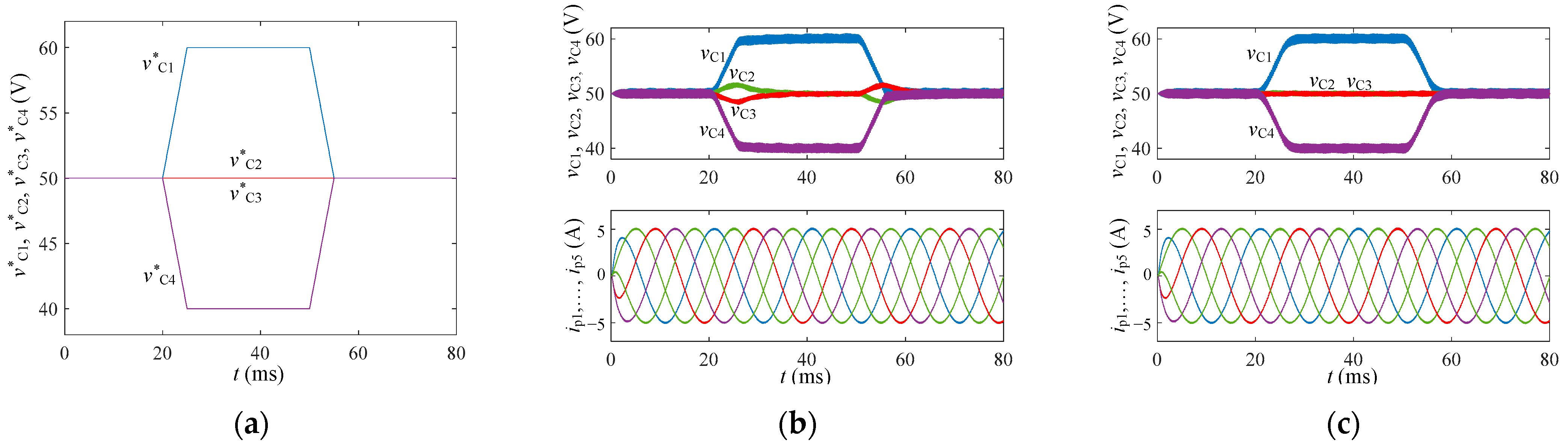
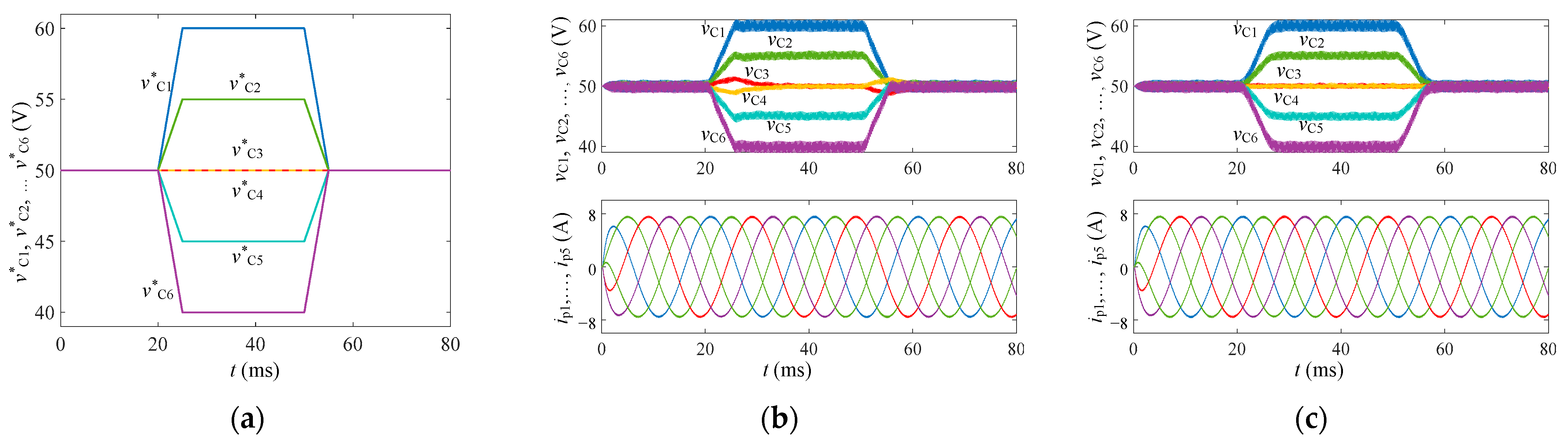
Figure 10 shows the performance under a five-level, five-phase system to prove the applicability of the proposed control to systems with a higher number of levels and legs. Similar to Figure 9, two ramps are generated in v*C1 and v*C4 commands. With the use of the proposed control, vC2 and vC3 remain constant over the transients, as desired. In a similar manner, Figure 11 further proves the good performance under a seven-level, five-phase system.
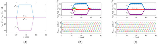
Figure 10.
Simulation results under ramp variations of the v*C1 and v*C4 commands of a five-level, five-phase system. Conditions: Vdc = 200 V, m = 0.5, C = 200 µF, R = 10 Ω, L = 10 mH, fs = 5 kHz, Gc(s) = 0.02/[1 + s/(1000π)]. (a) Capacitor voltage command values. (b) Control in [5] without decoupling. (c) Proposed inherently decoupled control from Figure 3, which is exactly equivalent to the control in [5] with decoupling.
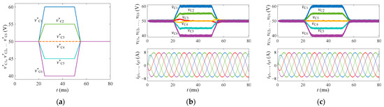
Figure 11.
Simulation results under ramp variations of the v*C1, v*C2, v*C5, and v*C6 commands of a seven-level, five-phase system. Conditions: Vdc = 300 V, m = 0.5, C = 270 µF, R = 10 Ω, L = 10 mH, fs = 5 kHz, Gc(s) = 0.02/[1 + s/(1000π)]. (a) Capacitor voltage command values. (b) Control in [5] without decoupling. (c) Proposed inherently decoupled control from Figure 3, which is exactly equivalent to the control in [5] with decoupling.
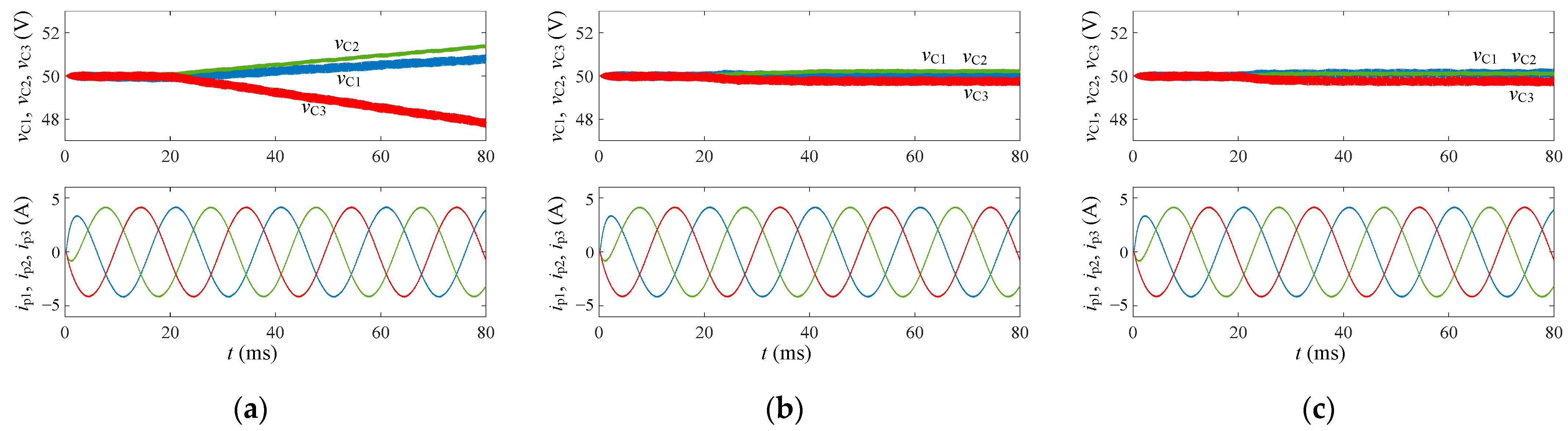
The simulation in Figure 12 is performed in the same conditions as in Figure 9 and demonstrates the control robustness against variations in the dc-link capacitor values. In this case, the capacitance of C2 is increased by 20%, while the capacitance of C3 is decreased by the same amount. Even with this large variation, the proposed decoupled system response shown in Figure 12c remains mostly unchanged and is superior to the non-decoupled control from Figure 9b and Figure 12b.
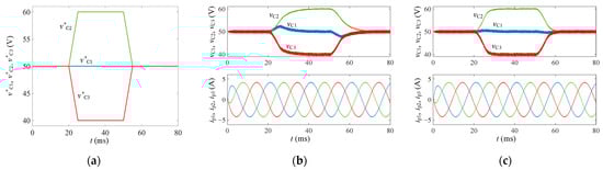
Figure 12.
Simulation results under ramp variations of the v*C2 and v*C3 commands of a four-level, three-phase system with unbalanced dc-link capacitor values. Conditions: Vdc = 150 V, m = 0.5, C1 = 155 µF, C2 = 186 µF, C3 = 124 µF, R = 10 Ω, L = 10 mH, switching frequency fs = 5 kHz, and Gc(s) = 0.02/[1 + s/(1000π)]. (a) Capacitor voltage command values. (b) Control in [5] without decoupling. (c) Proposed inherently decoupled control from Figure 3, which is exactly equivalent to the control in [5] with decoupling.
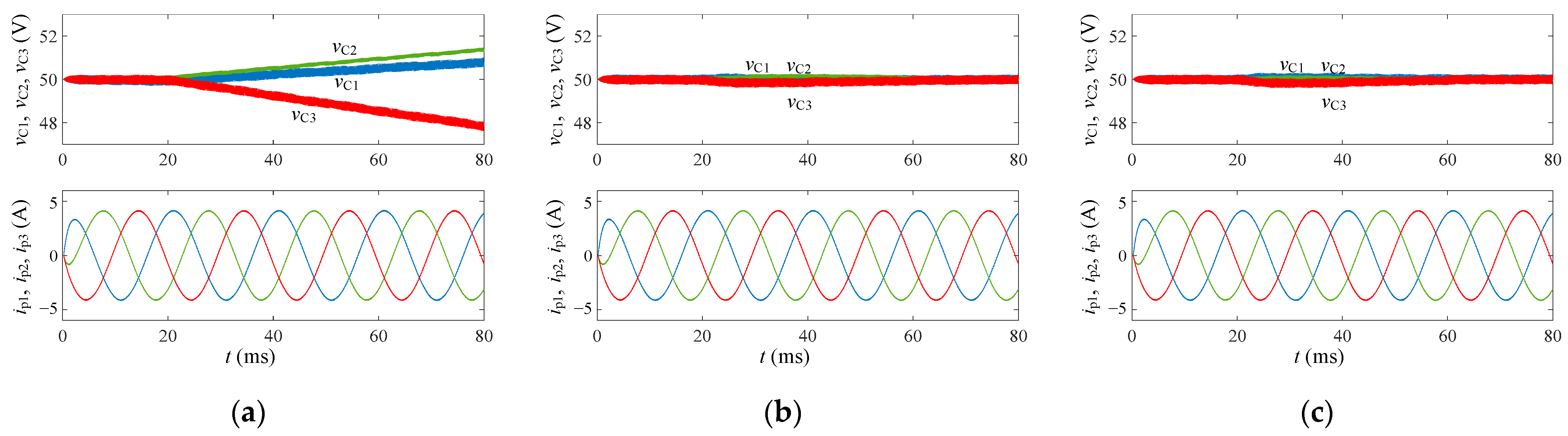
Figure 13 and Figure 14 verify the good system performance against unbalances in the dc-link capacitor leakage currents, emulated through a resistor in parallel with each capacitor. At the beginning of the simulations, the resistance value is the same for all of the capacitors with a value of 100 kΩ. At t = 20 ms, the resistance in parallel with capacitor C3 is reduced to 2 kΩ. When the control is not active, as in Figure 13a and Figure 14a, the capacitor voltages divert rapidly. However, in the cases where the control is active, as in Figure 13b,c and Figure 14b,c, the capacitor voltages remain stable. Figure 13b,c shows that with both controls, a small steady-state error remains in the capacitor voltages, as only a proportional compensator with moderate gain is being employed. In Figure 14b,c, a proportional–integral compensator is employed, which completely eliminates this steady-state error for both the decoupled and non-decoupled control cases.
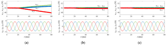
Figure 13.
Simulation results under unbalanced capacitor leakage currents of a four-level, three-phase system with a proportional compensator. Conditions: Vdc = 150 V, m = 0.5, C = 465 µF, RC1__leakage = 100 kΩ, RC2__leakage = 100 kΩ, RC3__leakage = 2 kΩ, R = 10 Ω, L = 10 mH, switching frequency fs = 5 kHz, and Gc(s) = 0.02/[1 + s/(1000π)]. (a) Control disabled. (b) Control in [5] without decoupling. (c) Proposed inherently decoupled control from Figure 3, which is exactly equivalent to the control in [5] with decoupling.
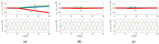
Figure 14.
Simulation results under unbalanced capacitor leakage currents of a four-level, three-phase system with a proportional–integral compensator. Conditions: Vdc = 150 V, m = 0.5, C = 465 µF, RC1__leakage = 100 kΩ, RC2__leakage = 100 kΩ, RC3__leakage = 2 kΩ, R = 10 Ω, L = 10 mH, switching frequency fs = 5 kHz, and Gc(s) = [0.02 + 1/s]/[1 + s/(1000π)]. (a) Control disabled. (b) Control in [5] without decoupling. (c) Proposed inherently decoupled control from Figure 3, which is exactly equivalent to the control in [5] with decoupling.
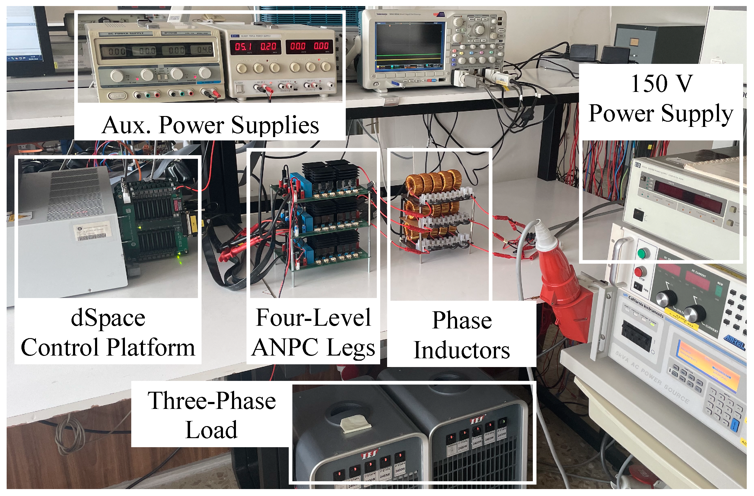
Experiments have also been carried out with a four-level, three-phase active-clamped dc–ac converter prototype built upon 100 V metal-oxide-semiconductor field-effect transistors and controlled with a dSPACE control platform, as shown in Figure 15. These experiments were performed under the same conditions as in Figure 9. The experimental results depicted in Figure 16 corroborate the corresponding simulation results from Figure 9.
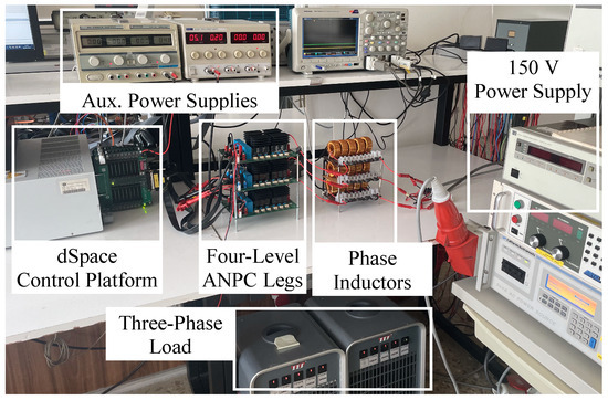
Figure 15.
Laboratory prototype of a three-phase, four-level NPC-based dc–ac converter.

4. Conclusions
The most effective and simple dc-link capacitor voltage balance control in NPC topologies is the one establishing n − 2 control loops regulating the voltage difference between neighbor capacitors. This control can be easily applied to any number of levels and features inherent decoupling among all control loops.
Reducing the complexity of the capacitor voltage control yields substantial benefits, directly influencing the system performance and enhancing its dynamic response, all while reducing the computational burden. The benefits in terms of computational cost increase with the number of levels. At the same time, the resulting reduced complexity decreases the required expertise for the implementation of multilevel converters, thereby facilitating their market adoption. The robustness of the proposed decoupling method is verified against different nonidealities. The precise regulation of the capacitor voltages of the proposed balancing control, in combination with a virtual vector pulsewidth modulation, enables the possibility to operate with multiple different capacitor voltage values along the converter dc-link without introducing low-frequency harmonic distortion in the converter ac voltages and currents.
The main limitation of this balancing method is that the maximum value of the neutral-point current idck that the converter can inject depends on the value of the converter leg output current ip and on the value of the converter modulation index. The lower the output leg current and the higher the modulation index, the lower the regulation margin. Thus, the regulation margin has some limits. This regulation margin also depends on the number of balancing control loops enabled and the sign and value of their commands [12]. One possible future research topic is to study how to optimally distribute this regulation margin among the different balancing control loops.
Author Contributions
Conceptualization, G.G.-R. and S.B.-M.; methodology, G.G.-R. and S.B.-M.; software, J.M.C.-S.; validation, R.G., J.M.C.-S. and S.B.-M.; formal analysis, R.G.; investigation, S.B.-M.; resources, S.B.-M.; writing—original draft preparation, S.B.-M.; writing—review and editing, S.B.-M., G.G.-R., R.G., J.M.C.-S.; supervision, S.B.-M.; project administration, S.B.-M.; funding acquisition, S.B.-M. All authors have read and agreed to the published version of the manuscript.
Funding
This work was supported by the European Union’s Horizon Europe research and innovation program under grant agreement No. 101056781. Views and opinions expressed are however those of the authors only and do not necessarily reflect those of the European Union or CINEA. Neither the European Union nor the granting authority can be held responsible for them. This work was supported in part by the Generalitat de Catalunya under Grant 2021 SGR 00376.
Data Availability Statement
The original contributions presented in the study are included in the article, further inquiries can be directed to the corresponding author.
Conflicts of Interest
The authors declare no conflicts of interest. The funders had no role in the design of the study; in the collection, analyses, or interpretation of data; in the writing of the manuscript; or in the decision to publish the results.
References
- Kouro, S.; Malinowski, M.; Gopakumar, K.; Pou, J.; Franquelo, L.G.; Wu, B.; Rodriguez, J.; Perez, M.A.; Leon, J.I. Recent advances and industrial applications of multilevel converters. IEEE Trans. Ind. Electron. 2010, 57, 2553–2580. [Google Scholar] [CrossRef]
- Akagi, H. Multilevel Converters: Fundamental Circuits and Systems. Proc. IEEE 2017, 105, 2048–2065. [Google Scholar] [CrossRef]
- Leon, J.I.; Vazquez, S.; Franquelo, L.G. Multilevel converters: Control and modulation techniques for their operation and industrial applications. Proc. IEEE 2017, 105, 2066–2081. [Google Scholar] [CrossRef]
- Alepuz, S.; Busquets-Monge, S.; Nicolas-Apruzzese, J.; Filbà-Martínez, À.; Bordonau, J.; Yuan, X.; Kouro, S. A survey on capacitor voltage control in neutral-point-clamped multilevel converters. Electronics 2022, 11, 527. [Google Scholar] [CrossRef]
- Busquets-Monge, S.; Griñó, R.; Nicolas-Apruzzese, J.; Bordonau, J. Decoupled dc-link capacitor voltage control of dc-ac multilevel multileg converters. IEEE Trans. Ind. Electron. 2016, 63, 1344–1349. [Google Scholar] [CrossRef]
- Wu, M.; Wang, K.; Yang, K.; Konstantinou, G.; Li, Y.W.; Li, Y. Unified Selective Harmonic Elimination Control for Four-Level Hybrid-Clamped Inverters. IEEE Trans. Power Electron. 2020, 35, 11488–11501. [Google Scholar] [CrossRef]
- Wodajo, E.T.; Elbuluk, M.; Choi, S.; Abu-Rub, H. Hybrid dc link voltage balancing for two-leg five-level neutral point clamped inverter. In Proceedings of the IEEE Energy Conversion Congress and Exposition, Baltimore, MD, USA, 29 September–3 October 2019. [Google Scholar]
- Debnath, T.; Gopakumar, K.; Umanand, L.; Zielinski, D.; Rajashekara, K. A nine-level inverter with single dc-link and low-voltage capacitors as stacked voltage sources with capacitor voltage control irrespective of load power factor. IEEE Open J. Ind. Electron. Soc. 2022, 3, 522–536. [Google Scholar] [CrossRef]
- Wang, J.; Yuan, X.; Jin, B. Carrier-based closed-loop dc-link voltage balancing algorithm for four level NPC converters based on redundant level modulation. IEEE Trans. Ind. Electron. 2021, 68, 11707–11718. [Google Scholar] [CrossRef]
- Wang, K.; Zheng, Z.; Xu, L.; Li, Y. Neutral-Point Voltage Balancing Method for Five-Level NPC Inverters Based on Carrier-Overlapped PWM. IEEE Trans. Power Electron. 2021, 36, 1428–1440. [Google Scholar] [CrossRef]
- Busquets-Monge, S.; Maheshwari, R.; Nicolas-Apruzzese, J.; Lupon, E.; Munk-Nielsen, S.; Bordonau, J. Enhanced DC-link capacitor voltage balancing control of DC–AC multilevel multileg converters. IEEE Trans. Ind. Electron. 2015, 62, 2663–2672. [Google Scholar] [CrossRef]
- Cervone, A.; Brando, G.; Dordevic, O.; Pizzo, A.D.; Meo, S. An adaptive multistep balancing modulation technique for multipoint-clamped converters. IEEE Trans. Ind. Appl. 2020, 56, 465–476. [Google Scholar] [CrossRef]

Disclaimer/Publisher’s Note: The statements, opinions and data contained in all publications are solely those of the individual author(s) and contributor(s) and not of MDPI and/or the editor(s). MDPI and/or the editor(s) disclaim responsibility for any injury to people or property resulting from any ideas, methods, instructions or products referred to in the content. |
© 2024 by the authors. Licensee MDPI, Basel, Switzerland. This article is an open access article distributed under the terms and conditions of the Creative Commons Attribution (CC BY) license (https://creativecommons.org/licenses/by/4.0/).