
A Geometrically Scalable Lumped Model for Spiral Inductors in Radio Frequency GaN Technology on Silicon


Abstract
1. Introduction
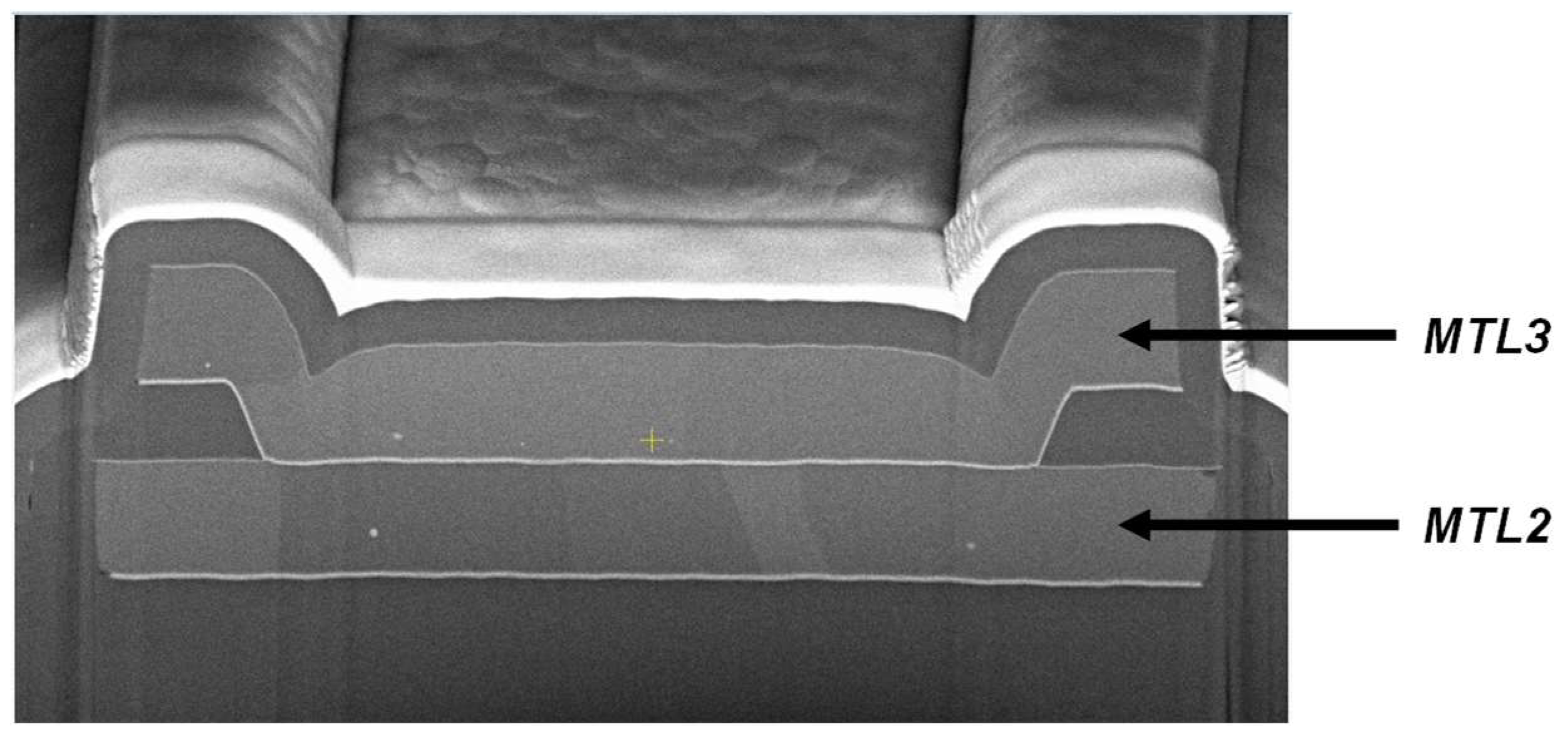
2. RF GaN Technology
3. Integrated Inductor Physics: Design Guidelines
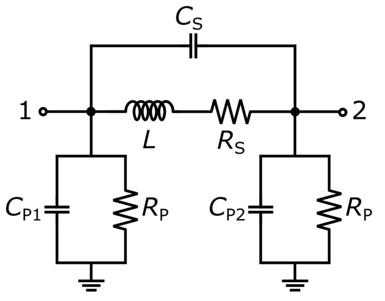
4. Geometrically Scalable Lumped Model Description
5. Model Validation
6. Conclusions
Author Contributions
Funding
Data Availability Statement
Conflicts of Interest
References
- Scuderi, A.; Ragonese, E.; Biondi, T.; Palmisano, G. Integrated Inductors and Transformers: Characterization, Design and Modeling for RF and MM-Wave Applications; CRC Press: Boca Raton, FL, USA; Taylor & Francis Group: Boca Raton, FL, USA, 2010. [Google Scholar]
- Ragonese, E.; Nocera, C.; Cavarra, A.; Papotto, G.; Spataro, S.; Palmisano, G. A Comparative analysis between standard and mm-wave optimized BEOL in a nanoscale CMOS technology. Electronics 2020, 9, 2124. [Google Scholar] [CrossRef]
- Salnikov, A.S.; Goryainov, A.E.; Dobush, I.M.; Kalentyev, A.A.; Garays, D.V. Approach to scalable modeling for planar inductor using EM simulation and a few samples measurement. In Proceedings of the 2017 IEEE MTT-S International Conference on Numerical Electromagnetic and Multiphysics Modeling and Optimization for RF, Microwave, and Terahertz Applications (NEMO), Seville, Spain, 17–19 May 2017; pp. 55–57. [Google Scholar]
- Dobush, I.M.; Vasil’evskii, I.S.; Zykov, D.D.; Bragin, D.S.; Salnikov, A.S.; Popov, A.A.; Gorelov, A.A.; Kargin, N.I. Development of a 0.15 μm GaAs pHEMT process design kit for low-noise applications. Electronics 2021, 10, 2775. [Google Scholar] [CrossRef]
- Eblabla, A.; Li, X.; Wallis, D.J.; Guiney, I.; Elgaid, K. High-performance MMIC inductors for GaN-on-low-resistivity silicon for microwave applications. IEEE Microw. Wirel. Compon. Lett. 2018, 28, 99–101. [Google Scholar] [CrossRef]
- Montesdeoca, M.S.M.; Angulo, S.M.; Duarte, D.M.; Del Pino, J.; García, J.A.G.Y.; Khemchandani, S.L. An analytical scalable lumped-element model for GaN on Si inductors. IEEE Access 2020, 8, 52863–52871. [Google Scholar] [CrossRef]
- Chander, S.; Bansal, K.; Gupta, S.; Gupta, M. Design and analysis of high performance air-bridge spiral circular inductors for GaN MMICs up to Ku band. In Proceedings of the 2017 Devices for Integrated Circuit (DevIC), Kalyani, India, 23–24 March 2017; pp. 734–736. [Google Scholar]
- Chander, S.; Bansal, K.; Gupta, S.; Gupta, M. Design and analysis of spiral circular inductors for GaN based low noise amplifier (MMICs). In Proceedings of the 2015 International Conference on Microwave, Optical and Communication Engineering (ICMOCE), Bhubaneswar, India, 18–20 December 2015; pp. 292–294. [Google Scholar]
- Wang, H.-S.; He, W.-L.; Wang, R.-D.; Zhang, M.-H. A double-π equivalent circuit model for GaN on-chip inductors. In Proceedings of the IEEE International Conference on Solid-State and Integrated Circuit Technology, Hangzhou, China, 25–28 October 2016; pp. 811–815. [Google Scholar]
- Long, J.R.; Copeland, M.A. The modeling, characterization, and design of monolithic inductors for silicon RF IC’s. IEEE J. Solid-State Circuits 1997, 32, 357–369. [Google Scholar] [CrossRef]
- Kapur, S.; Long, D.E. Modeling of integrated RF passive devices. In Proceedings of the IEEE Custom Integrated Circuits Conference, San Jose, CA, USA, 19–22 September 2010; pp. 1–8. [Google Scholar]
- Cavarra, A.; Nocera, C.; Papotto, G.; Ragonese, E.; Palmisano, G. Transformer design for 77-GHz down-converter in 28-nm FD-SOI CMOS technology. In Applications in Electronics Pervading Industry, Environment and Society, ApplePies 2018; Saponara, S., De Gloria, A., Eds.; Lecture Notes in Electrical Engineering; Springer: Cham, Switzerland, 2019; Volume 573. [Google Scholar]
- Huo, X.; Chan, P.C.H.; Chen, K.J.; Luong, H.C. A physical model for on-chip spiral inductors with accurate substrate modeling. IEEE Trans. Electron Devices 2006, 53, 2942–2949. [Google Scholar] [CrossRef]
- Sia, C.B.; Ong, B.H.; Chan, K.W.; Yeo, K.S.; Ma, J.G.; Do, M.A. Physical layout design optimization of integrated spiral inductors for silicon-based RFIC applications. IEEE Trans. Electron Devices 2005, 52, 2559–2567. [Google Scholar] [CrossRef]
- Biondi, T.; Scuderi, A.; Ragonese, E.; Palmisano, G. Characterization and modeling of silicon integrated spiral inductors for high-frequency applications. Analog. Integr. Circuits Signal Process. 2007, 51, 89–100. [Google Scholar] [CrossRef]
- Ragonese, E.; Scuderi, A.; Biondi, T.; Palmisano, G. Scalable lumped modeling of single-ended and differential inductors for RF IC Design. Wiley Int. J. RF Microw. Comput.-Aided Eng. 2009, 19, 110–119. [Google Scholar]
- Biondi, T.; Scuderi, A.; Ragonese, E.; Palmisano, G. Analysis and modeling of layout scaling in silicon integrated stacked transformers. IEEE Trans. Microw. Theory Tech. 2006, 54, 2203–2210. [Google Scholar] [CrossRef]
- El-Gharniti, O.; Kerherve, E.; Begueret, J.-B. Modeling and characterization of on-chip transformers for silicon RFIC. IEEE Trans. Microw. Theory Tech. 2007, 55, 607–615. [Google Scholar] [CrossRef]
- Cerantonio, V.; Giuffrida, M.; Miccoli, C.; Chini, A.; Iucolano, F. From T-CAD simulations to large signal model for GaN RF device. In Proceedings of the 2020 AEIT International Conference of Electrical and Electronic Technologies for Automotive (AEIT AUTOMOTIVE), Turin, Italy, 8–10 November 2020; pp. 1–6. [Google Scholar]
- Giorgino, G.; Cioni, M.; Miccoli, C.; Gervasi, L.; Giuffrida, M.F.S.; Ruvolo, M.; Castagna, M.E.; Cappellini, G.; Luongo, G.; Moschetti, M.; et al. Study of 100V GaN power devices in dynamic condition and GaN RF device performances in sub-6GHz frequencies. Elsevier E-Prime Adv. Electr. Eng. Electron. Energy 2023, 6. [Google Scholar] [CrossRef]
- Vandendaele, W.; Leurquin, C.; Lavieville, R.; Jaud, M.A.; Viey, A.G.; Gwoziecki, R.; Mohamad, B.; Nowak, E.; Constant, A.; Iucolano, F. Reliability of GaN MOSc-HEMTs: From TDDB to threshold voltage instabilities (Invited). In Proceedings of the IEEE International Reliability Physics Symposium (IRPS), Monterey, CA, USA, 26–30 March 2023; pp. 1–8. [Google Scholar]
- Scandurra, A.; Testa, M.; Franzò, G.; Greco, G.; Roccaforte, F.; Castagna, M.E.; Calabretta, C.; Severino, A.; Iucolano, F.; Bruno, E.; et al. Isolation of bidimensional electron gas in AlGaN/GaN heterojunction using Ar ion implantation. Mater. Sci. Semicond. Process. 2023, 168, 107871. [Google Scholar] [CrossRef]
- Santhakumar, R.; Pei, Y.; Mishra, U.K.; York, R.A. Monolithic millimeter-wave distributed amplifiers using AlGaN/GaN HEMTs. In Proceedings of the IEEE MTT-S Int. Microwave Symposium Digest, Atlanta, GA, USA, 15–20 June 2008; pp. 1063–1066. [Google Scholar]
- Korndorfer, F.; Muhlhaus, V. Lumped modeling of integrated MIM capacitors for RF applications. In Proceedings of the Microwave Measurement Conference (ARFTG), Austin, TX, USA, 8–9 December 2016; pp. 1–4. [Google Scholar]
- Bevilacqua, A. Fundamentals of integrated transformers: From principles to applications. IEEE Solid-State Circuits Mag. 2020, 12, 86–100. [Google Scholar] [CrossRef]
- Long, J.R. Monolithic transformers for silicon RF IC design. IEEE J. Solid-State Circuits 2000, 35, 1368–1382. [Google Scholar] [CrossRef]
- Giammello, V.; Ragonese, E.; Palmisano, G. Transmitter chipset for 24/77-GHz automotive radar sensors. In Proceedings of the IEEE Radio Frequency Integrated Circuits Symposium (RFIC) Technical Digest, Anaheim, CA, USA, 23–25 May 2010; pp. 75–78. [Google Scholar]
- Nocera, C.; Papotto, G.; Cavarra, A.; Ragonese, E.; Palmisano, G. A 13.5-dBm 1-V power amplifier for W-band automotive radar applications in 28-nm FD-SOI CMOS technology. IEEE Trans. Microw. Theory Tech. 2021, 69, 1654–1660. [Google Scholar] [CrossRef]
- Papotto, G.; Nocera, C.; Finocchiaro, A.; Parisi, A.; Cavarra, A.; Castorina, A.; Ragonese, E.; Palmisano, G. A 27-mW W-band radar receiver with effective TX leakage suppression in 28-nm FD-SOI CMOS. IEEE Trans. Microw. Theory Tech. 2021, 69, 4132–4141. [Google Scholar] [CrossRef]
- Kuhn, W.B.; Ibrahim, N.M. Approximate analytical modeling of current crowding effects in multi-turn spiral inductors. In Proceedings of the 2000 IEEE MTT-S International Microwave Symposium Digest, Boston, MA, USA, 11–16 June 2000; pp. 405–408. [Google Scholar]
- Craninckx, J.; Steyaert, M.S.J. A 1.8-GHz low-phase-noise CMOS VCO using optimized hollow spiral inductors. IEEE J. Solid State Circuits 1997, 32, 736–744. [Google Scholar] [CrossRef]
- Greco, N.; Parisi, A.; Lombardo, P.; Spina, N.; Ragonese, E.; Palmisano, G. A double-isolated dc–dc converter based on integrated LC resonant barriers. IEEE Trans. Circuits Syst. I Reg. Pap. 2018, 65, 4423–4433. [Google Scholar] [CrossRef]
- Greco, N.; Parisi, A.; Spina, N.; Ragonese, E.; Palmisano, G. Scalable lumped models of integrated transformers for galvanically isolated power transfer systems. Integration 2018, 63, 323–331. [Google Scholar] [CrossRef]
- Keysight Helpfiles. PCB Material Characterization. Available online: https://helpfiles.keysight.com/csg/N1930xB/ToolsAndUtilities/PCB_Material_Characterization.htm#The_Svensson-Djordjevic_Model (accessed on 3 June 2024).
- Kuhn, W.B.; Ibrahim, N.M. Analysis of current crowding effects in multiturn spiral inductors. IEEE Trans. Microw. Theory Tech. 2001, 49, 31–38. [Google Scholar] [CrossRef]
- Kuhn, W.B. Loss mechanisms and quality factor improvement for inductors in high-resistivity SOI processes. In Proceedings of the IEEE 12th Topical Meeting on Silicon Monolithic Integrated Circuits in RF Systems, Santa Clara, CA, USA, 16–18 January 2012; pp. 29–32. [Google Scholar]
- Kuhn, W.B.; He, S.; Mojarrad, M. Modeling spiral inductors in SOS processes. IEEE Trans. Electron Devices 2004, 51, 677–683. [Google Scholar] [CrossRef]
- Mohan, S.S.; del Mar Hershenson, M.; Boyd, S.P.; Lee, T.H. Simple accurate expressions for planar spiral inductances. IEEE J. Solid-State Circuits 1999, 34, 1419–1424. [Google Scholar] [CrossRef]
- Mohan, S.S. The Design, Modeling and Optimization of on Chip Inductor and Transformer Circuit. Ph.D. Thesis, Stanford University, Stanford, CA, USA, 1999. [Google Scholar]


| Inductors | 1 | 2 | 3 | 4 | 5 | 6 | 7 | 8 | 9 | 10 |
|---|---|---|---|---|---|---|---|---|---|---|
| w [μm] | 10 | 10 | 20 | 20 | 40 | 40 | 60 | 60 | 100 | 100 |
| n | 3.5 | 6.5 | 1.5 | 3.5 | 1.5 | 2.5 | 1.5 | 2.5 | 1.5 | 1.5 |
| din [μm] | 60 | 60 | 220 | 150 | 120 | 200 | 290 | 240 | 100 | 300 |
| Errors | Maximum | Minimum |
|---|---|---|
| L @ 100 MHz | 9.2% | 1.7% |
| QMAX | 16.4% | 3.6% |
| SRF | 12.3% | 0.3% |
Disclaimer/Publisher’s Note: The statements, opinions and data contained in all publications are solely those of the individual author(s) and contributor(s) and not of MDPI and/or the editor(s). MDPI and/or the editor(s) disclaim responsibility for any injury to people or property resulting from any ideas, methods, instructions or products referred to in the content. |
© 2024 by the authors. Licensee MDPI, Basel, Switzerland. This article is an open access article distributed under the terms and conditions of the Creative Commons Attribution (CC BY) license (https://creativecommons.org/licenses/by/4.0/).
Share and Cite
Spataro, S.; Sapone, G.; Giuffrida, M.; Ragonese, E. A Geometrically Scalable Lumped Model for Spiral Inductors in Radio Frequency GaN Technology on Silicon. Electronics 2024, 13, 2665. https://doi.org/10.3390/electronics13132665
Spataro S, Sapone G, Giuffrida M, Ragonese E. A Geometrically Scalable Lumped Model for Spiral Inductors in Radio Frequency GaN Technology on Silicon. Electronics. 2024; 13(13):2665. https://doi.org/10.3390/electronics13132665
Chicago/Turabian StyleSpataro, Simone, Giuseppina Sapone, Marcello Giuffrida, and Egidio Ragonese. 2024. "A Geometrically Scalable Lumped Model for Spiral Inductors in Radio Frequency GaN Technology on Silicon" Electronics 13, no. 13: 2665. https://doi.org/10.3390/electronics13132665
APA StyleSpataro, S., Sapone, G., Giuffrida, M., & Ragonese, E. (2024). A Geometrically Scalable Lumped Model for Spiral Inductors in Radio Frequency GaN Technology on Silicon. Electronics, 13(13), 2665. https://doi.org/10.3390/electronics13132665