Article

An Analog Delay-Locked Loop with Digital Coarse Lock Incorporating Error Compensation for Fast and Robust Locking

1
School of Electronic Engineering, Engineering Research Institute (ERI), Gyeongsang National University, Jinju 52828, Republic of Korea
2
Department of Semiconductor Systems Engineering, Sejong University, Seoul 05006, Republic of Korea
3
Department of Electronic Engineering, Hanbat National University, Daejeon 34158, Republic of Korea
*
Author to whom correspondence should be addressed.
These authors contributed equally to this work.
Electronics 2024, 13(13), 2514; https://doi.org/10.3390/electronics13132514
Submission received: 22 May 2024 / Revised: 17 June 2024 / Accepted: 25 June 2024 / Published: 27 June 2024
(This article belongs to the Special Issue Advances in Analog and Mixed-Signal Integrated Circuits)

Abstract

:
This paper presents an analog delay-locked loop (DLL) with a digital coarse lock and error compensation, designed to enhance locking speed in duty-cycled operation while ensuring reliability. To accelerate coarse locking speed and prevent coarse lock failure, the proposed DLL combines a low-resolution digital-to-analog converter (DAC) with an analog method for accurate lock range identification, efficiently handling scenarios where the DAC’s limited resolution could lead to failure. Additionally, it enables the rapid control of voltage adjustments by disconnecting a loop filter during the coarse lock, eliminating the need for a buffer. The DLL improves the coarse lock process reliability by compensating for potential false lock errors caused by circuit non-idealities, such as residual RC delay and amplifier offset. Furthermore, it reuses the previously identified DAC input for the duty-cycled operation to significantly reduce relock time. To mitigate the risk of potential false lock resulting from changes in locking conditions, it can update the previous DAC input upon relocking, ensuring more reliable relocking. The proposed DLL, implemented in a 28 nm CMOS process, reduces initial lock and relock times by an average of 49.3% and 65.9% at a supply voltage of 0.5 V, and 42.4% and 70.2% at 1 V, respectively, compared to the conventional analog DLL.

1. Introduction

In neural network hardware, analog multiplier accumulators often utilize pulse width modulation (PWM) to convert multi-bit digital inputs into time-domain signals [1,2,3] (Figure 1a). Increasing the clock frequency (fCLK) is a straightforward approach to enhance PWM resolution and achieve higher throughput. However, multiphase clock generators, such as phase-locked loops (PLLs) [4,5] or delay-locked loops (DLLs) [6,7,8,9,10,11,12,13,14,15,16,17,18,19,20,21,22,23], provide a potentially more power-efficient alternative without increasing the fCLK (Figure 1b). If frequency multiplication is unnecessary, DLLs may be preferable to PLLs because they provide better jitter performance and stability [6,7,8,9,10]. However, DLLs, particularly those with a wide range, can cause multiphase clock malfunctions due to false lock issues [11], such as harmonic or stuck false locks, depending on their initial delay. Also, since the PWM in in-memory or near-memory computing can be performed in a duty-cycled manner [1,2,3], energy efficiency can be improved by operating DLLs in duty-cycled mode instead of keeping them always on. Thus, a false-locking-free DLL with fast relocking is beneficial for energy-efficient PWM.
DLLs can be classified into analog and digital according to their delay line control method. Compared with digital DLLs, analog DLLs generally provide better jitter characteristics, smaller static phase offsets, and more precise multiphase generation due to their continuous delay control [12,13]. However, analog DLLs typically have a slower locking speed than digital DLLs. This is because, unlike analog DLLs, digital DLLs can directly adopt fast lock point search algorithms, such as successive approximation register (SAR) logic [12].
To prevent false locks, the initial delay of the delay line (TDL) must satisfy the following condition (i.e., coarse lock) [6] before starting the DLL locking process:
0.5 · T R E F < T D L < 1.5 · T R E F
where TREF is the period of the reference clock (CLKREF). In conventional analog DLLs (Figure 2a), the control voltage (VC) of the voltage-controlled delay line (VCDL) is initially set to the supply voltage (VDD) to achieve the minimum delay. Then, VC is gradually decreased by using an additional current source (IB) to find the suitable condition for TDL. However, while increasing IB can accelerate the overall lock time, including initial TDL adjustment, it may cause overly rapid changes in VC. These rapid changes may fail to meet (1) due to nonlinear VCDL phase gain, increasing lock failure rate, as indicated in Monte Carlo simulation results (Figure 2b).
Various architectures have been proposed to accelerate the lock time without the false lock issues. The analog DLL with multiple loops [15] can shorten lock time by starting from a nearly locked state, utilizing the VC from the locked reference loop (Figure 3a). However, an offset in the unity-gain buffer and mismatches between loops can decelerate locking. An analog DLL with a digital-controlled delay line (DCDL) [12] can achieve both a fast lock and false lock avoidance by employing SAR logic before fine lock using VCDL (Figure 3b). Yet, it increases the design complexity due to two distinct types of delay lines and may not be suitable for multiphase generation since VCDL and DCDL are separated. Similarly, an analog DLL with a time-to-digital converter (TDC) and a digital-to-analog converter (DAC) [17] can also achieve a fast coarse lock and a wide operational range free from false locks by applying quantized voltages to VCDL (Figure 3c). However, this may require a high-bit DAC to find a suitable quantization voltage that fulfills (1) [20,21]. While using exponential steps rather than linear ones in the DAC reduces the required bit number, a low-dropout regulator (or a unity-gain buffer) can still be needed during the coarse lock to supply the VCDL (or to handle the loop filter’s large capacitance) [17].
This paper presents an analog DLL featuring a digital coarse lock with error compensation, which enables fast locking for duty-cycled operation. The DLL identifies the coarse lock range satisfying (1) through a linear search algorithm with a low-resolution DAC. Even if the initial search fails due to the DAC’s coarse resolution, the DLL can fine-tune the VC in an analog manner to meet (1) from the quantization voltage closest to the required TDL condition. Moreover, by disconnecting the loop filter with large capacitance during the coarse lock process, the DLL allows rapid VC adjustments without needing a unity-gain buffer, thus speeding up the coarse lock time. The buffer is activated only when charging the loop filter. It also compensates for errors caused by circuit non-idealities, such as parasitic RC delay or amplifier offset, reducing the risk of lock failure. The rest of the paper is organized as follows: Section 2 introduces the proposed architecture, Section 3 describes the circuit implementation, Section 4 presents the simulation and measurement results, and Section 5 concludes this work.

2. Architecture

Figure 4 presents a block diagram of the proposed DLL, which includes a conventional analog DLL, phase range detector (PRD), digital control block, DAC, unity-gain buffer, and switch controller for the VC tuning. The proposed DLL’s locking process is divided into coarse lock and fine lock. The coarse lock employs the DAC and an analog tuning method to find an appropriate VC satisfying (1), followed by the fine lock with the phase detector in the analog DLL. As depicted in Figure 5, the overall lock process comprises three key states: the phase range detection state, loop filter charging state, and analog DLL state. Initially, in the phase range detection state, the PRD classifies the VCDL delay (TVCDL) phase range into three groups:
U n d e r   R a n g e :         T V C D L 0.5 · T R E F + T m , u n d e r
L o c k   R a n g e : 0.5 · T R E F + T m , u n d e r < T V C D L 1.5 · T R E F T m , o v e r
O v e r   R a n g e : T V C D L > 1.5 · T R E F T m , o v e r
where T m , u n d e r and T m , o v e r are the timing margins for the under range and the over range, respectively.
The PRD uses multiple phases based on these timing margins (which will be discussed in Section 3.1). During this state, the DLL incrementally increases the TVCDL from the minimum delay to achieve the lock range (i.e., linear search). Accordingly, the DAC’s digital input (DIN) starts at its maximum value, decreasing by 1 LSB from its previous DIN to increase the TVCDL whenever the PRD indicates the under range. To quickly apply DIN adjustments to the TVCDL, the DAC’s output resistance should be sufficiently low, given the high capacitance of the loop filter. This requirement increases the DAC’s power consumption due to the need for an output buffer. To reduce power consumption, the DLL temporarily disconnects the loop filter during this state, achieving a 90% reduction in capacitance at the DAC output, as confirmed by post-layout simulation, and eliminating the buffer requirement [24].
When the PRD output transitions from the under range to the lock range, the phase range detection state completes, indicating that the DLL has successfully identified the suitable DIN value for the lock range (Figure 6a). Identifying the lock range across a wide CLKREF typically requires a high-resolution DAC for fine TVCDL control. However, this may slow the coarse lock process due to the increased number of voltage levels, adding to the design complexity. Conversely, a low-resolution DAC can accelerate the coarse lock process but may not always identify the lock range due to coarse TVCDL control. To relax this trade-off, the proposed DLL employs an analog tuning method in the subsequent state, which is detailed later in this section, to fine-tune the VC for the lock range. This approach efficiently identifies the lock range without the high-resolution DAC, simplifying the design. If the PRD output jumps directly from the under range to the over range, bypassing the lock range due to the low-resolution DAC, the search is halted. The DIN corresponding to the over range then increases by 1 LSB. This adjustment returns the DIN to its previous value, positioning the TVCDL within the under range and close to the lock range, thereby completing the current state as the under-range condition (Figure 6b).
In the loop filter charging state, the loop filter is reconnected and charged through the unity-gain buffer with the DAC output voltage corresponding to the final DIN value from the phase range detection state. After the predefined charging cycles are complete, the DLL transitions to the analog DLL state. Before describing the subsequent state, it is important to note two primary causes of potential lock failure: parasitic RC delay in the phase range detection state and buffer offset (or insufficient charging cycles) in the loop filter charging state.
Even though disconnecting the loop filter in the phase range detection state significantly reduces its capacitance, residual capacitance and resistance still introduce a delay in this state, which is particularly noticeable as TREF decreases. In the phase range detection state, the actual TVCDL can be less than the ideal value due to the RC delay at the input node of the VCDL, which elevates the average VC level above the ideal DAC output level. However, if an ideal buffer is used, the VC level in the loop filter charging state is precisely charged to the desired ideal level. Therefore, the PRD output of the loop filter charging state can differ from that of the phase range detection state (Figure 7a), potentially leading to lock failure. For example, even when the DIN corresponding to the lock range is successfully identified in the phase range detection state, harmonic lock can occur if the TVCDL falls into the over range in the loop filter charging state. This issue arises from an underestimation of the phase range, which can be attributed to the RC delay previously mentioned.
Additionally, even in the absence of RC delay in the phase range detection state, a similar problem can arise from buffer offset (or insufficient charging cycles) in the loop filter charging state. A negative offset (or insufficient cycles) can induce the over-range condition by increasing the TVCDL (Figure 7b).
In the analog DLL state, operation depends on the phase range induced by the actual VC after the loop filter charging state. There are three cases: (1) If the PRD output indicates the under range, the switch controller initiates the VC tuning step by turning on IB to gradually increase the TVCDL. Once the PRD output reaches the lock range, the switch controller turns off IB. Subsequently, the proposed DLL completes the VC tuning step and transitions to the fine lock step. (2) If the PRD output indicates the lock range, the fine lock step is immediately initiated using the phase detector. (3) If the over-range condition is detected, the proposed DLL transitions back to the loop filter charging state by increasing the DIN by 1 LSB to reduce the TVCDL. This action aims to exit the over-range condition and achieve either the under-range or lock-range conditions. It then transitions back to the analog DLL state to reclassify the phase range of the reduced TVCDL. Even if a delay error greater than 2 LSBs occurs, causing the over-range condition, this sequence repeats until the PRD output indicates the under range or lock range. This initiates the VC tuning step if the under-range condition is detected or the fine lock step if the lock-range condition is detected. Consequently, the proposed DLL can lock to CLKREF without encountering the false lock issue.
Furthermore, whenever the DLL restarts after achieving the initial lock in the duty-cycled operation, the previous final DIN can generally be reused to bypass the phase range detection state, significantly reducing the relock time. However, if the locking conditions have changed between the previous lock and the restart, the reused DIN may lead to the over-range condition, making the reused DIN unsuitable (Figure 7c). In such cases, the DLL updates the DIN using the same compensation strategy as described earlier, ensuring a reliable relock process. In conclusion, the proposed architecture achieves fast locking without the risk of false locks, even when utilizing a low-resolution DAC.

3. Circuit Implementation

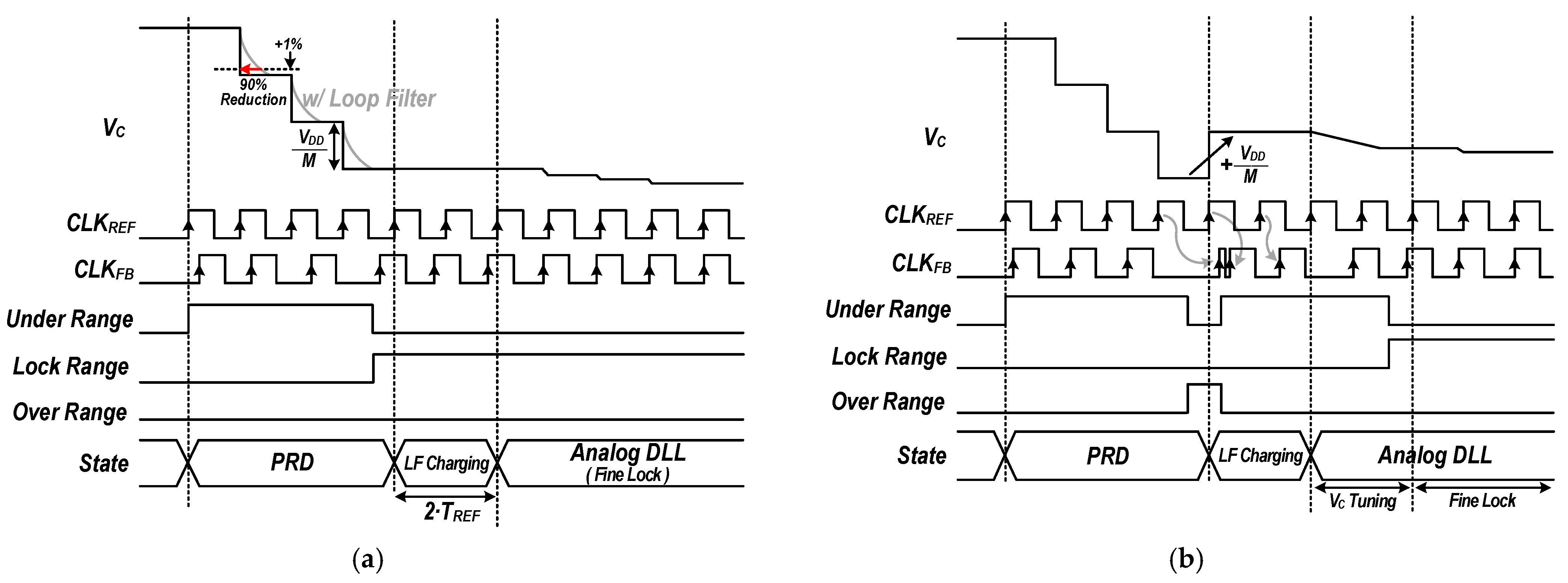
3.1. Phase Range Detector

Figure 8a,b illustrate the proposed PRD circuit and the defined ranges, respectively. These defined ranges, as specified in (2)–(4), are determined by the positions of the feedback clock (CLKFB) relative to the phase of CLKREF. The PRD captures CLKREF at the rising edges of the DLL’s multiphase outputs using D flip-flops (DFFs) [25]. The outputs Q [11:1] from these DFFs enable combinational logic to classify the TVCDL into the lock range, under range, or over range. For the VCDL with M delay stages, the phase range of TVCDL can be determined by the AND gating of the Nth Q (=Q [N]) and the inverted (N + 1)th Q (=Q [N + 1]), as follows:
M · D · T R E F N + 1 < T V C D L M · D · T R E F N
where D denotes the duty cycle of the CLKREF. To define the lock range, the phase range in (5) is extended by OR gating multiple AND gate outputs. In this work, with 50% duty cycled CLKREF, the lock range is defined as
8 11 · T R E F < T V C D L 4 3 · T R E F
This configuration sets the T m , u n d e r and the T m , o v e r in (3) to 5 / 22 · T R E F and 1 / 6 · T R E F , respectively. The values 5/22 and 1/6 were determined based on simulations and are intended to provide sufficient margin under typical PVT variations. Additionally, to guarantee T V C D L 1.6 · T R E F , the AND gating of Q [5:1] is included in the lock range logic. For the under range, the AND gating of Q [11:1] indicates the following range:
T V C D L 8 11 · T R E F
The over-range signal occurs when both the lock-range and the under-range signals are 0, identified by NOR gating.

3.2. DAC, Auto-Zero Buffer, and Voltage-Boosting Circuits (VBCs)

The DAC is designed with a resistor ladder structure using unary resistors and includes a footer transistor, which helps reduce static power consumption by deactivating the DAC when it is not in use (Figure 9). Although the proposed algorithm, presented in Section 2, can compensate for buffer offset error, an excessive offset may delay the locking process, as it requires additional time for compensation. Thus, the auto-zero technique is utilized for robust operation during the loop filter charging state. Even if some residual offset remains after auto-zeroing, the proposed algorithm can still compensate for it.
At a low VDD (e.g., 0.5 V), the DAC switches face challenges in turning on, leading to substantial signal-dependent delays in the phase range detection state. To address this, a voltage-boosting circuit [26] is used (Figure 10), enabling efficient switch operation with a smaller transistor size. These circuits can be manually disabled when VDD is sufficiently high.

3.3. Self-Resetting Phase Detector

Figure 11a,b show the proposed phase detector (PD) and its operations, respectively. Local feedback is employed for static logic design to ensure the PD’s reliable operation even at low frequencies of CLKREF, where dynamic circuits may face challenges. For the PD’s normal operation, the rising edge timing difference between CLKREF and CLKFB should be less than 0.5 · T R E F . When CLKREF leads (or lags) CLKFB, the pulse width of the UP (or DN) signal is proportional to the input phase difference while maintaining a low DN (or UP) signal. This single-output approach helps reduce the power consumption during the fine lock process by preventing short currents. However, the PD’s dead zone can worsen jitter performance due to its range of undetectable phase differences. To mitigate this, the PD is designed to generate short pulses for both UP and DN in the locked state, effectively reducing the dead zone [4].

3.4. Digital Building Blocks

The digital blocks, including the FSM, control logic, counter, and decoder, were designed with a hardware description language and synthesized with automated placement and routing. To ensure a 50% duty cycle for CLKREF, which is necessary for the normal operation of the PRD circuit, the external clock is halved. Additionally, these digital blocks support configurable options that allow for adjusting cycles as needed to accommodate the settling time required for VC changes due to DIN settings or for loop filter charging. To further reduce power consumption, clock gating is applied to these digital blocks.

4. Experimental Results

The proposed DLL was fabricated using a 28 nm CMOS process. The chip micrograph, shown in Figure 12, indicates that the core circuit occupies an active area of 0.013 mm2. As a building block of a low-power neural network system with a processing-in-memory architecture for biomedical applications (e.g., a standard clinical ECG application has a bandwidth of 0.05 Hz to 100 Hz), the DLL was designed to operate at a VDD of 0.5 V and within the CLKREF frequency range of several MHz, generating 16 multiphases.
To determine the minimum DAC level required for lock range detection without employing the analog tuning method, Monte Carlo simulations were conducted at various CLKREF frequencies and DAC levels under consistent conditions, including at the VDD of 0.5 V, and including both global and local process variations. The results, illustrated in Figure 13, show that the lock range detection rate increases with the DAC level, suggesting that a minimum of 30 levels is necessary for the given VDD.
Further Monte Carlo simulations were conducted to determine appropriate DAC levels when the analog tuning method is employed, focusing on the coarse lock time across different CLKREF frequencies and DAC levels (Figure 14). As expected, the mean coarse lock time tends to increase as the CLKREF frequency decreases at the same DAC levels because the VC required for the lock range also decreases at these lower frequencies.
Additionally, the simulations revealed that lower DAC levels initially reduce the mean coarse lock time, which can be attributed to the larger voltage step per LSB during the phase range detection state. However, if the DAC level is too low (e.g., five levels in Figure 14), this large voltage step can lead to severe over-range conditions at some CLKREF frequencies, resulting in excessive TVCDL. These conditions prolong the cycles for phase range detection because correct PRD outputs are only obtained after all PRD inputs have been updated.
Furthermore, as DAC levels continue to decrease, the lock range detection rate, using only the DAC, drops. This necessitates an increase in the average number of cycles required for the analog tuning method. Therefore, using excessively low DAC levels can ultimately result in increased coarse lock time. Additionally, the standard deviations (σ), as seen in Figure 14, tend to increase as the DAC level decreases, indicating more frequent activation of the analog tuning method. Based on these findings, the prototype employed seven DAC levels with the VDD of 0.5 V.
Figure 15a,b show the measured DLL output and state transitions for scenarios without and with error compensation, respectively, confirming alignment with the previously described timing diagrams. These measurements were conducted using a core VDD of 0.5 V and an I/O VDD of 0.7 V. The CLKREF frequency was set at 0.75 MHz for the former scenario and 1.25 MHz for the latter.
Figure 16a,b show the measured lock times for various CLKREF frequencies at core VDDs of 0.5 V and 1 V, respectively. By disabling the digital coarse lock feature, the proposed DLL can function as the conventional analog DLL, allowing for direct comparisons that demonstrate the effectiveness of the proposed design; these results are summarized in Table 1. When the digital coarse lock feature is enabled, it significantly reduces both initial lock and relock times. On average, at a VDD of 0.5 V, initial lock time is reduced by 49.3% and relock time by 65.9%; at 1 V, the reductions are 42.4% for initial lock time and 70.2% for relock time, compared to those of the conventional analog DLL. Furthermore, the proposed DLL shows an average reduction in relock time over initial lock time by 32.7% at 0.5 V and 48.3% at 1 V, making it particularly suitable for applications requiring duty-cycled operations.
Figure 17 shows the simulated power breakdown under different VDD conditions during the coarse lock process, where the buffer, DAC, PRD, and digital control block are activated. It should be noted that the DAC and analog DLL dominate the overall power consumption across different frequencies of the CLKREF.
The external clock of the DLL, sourced from a waveform generator, is halved by the system’s main control block and routed through a synthesized clock tree, resulting in the CLKREF. This CLKREF has an RMS jitter of 16.64 ps at 40 MHz, which is the primary contributor to the DLL’s overall jitter. The DLL output exhibits an RMS jitter of 24.57 ps at a core VDD of 1 V (Figure 18).
The performance of the proposed DLL compared with previous works is summarized in Table 2, highlighting its fast locking time and comparable figure of merit (FoM) for power.

5. Conclusions

A false-lock-free analog DLL with digital coarse lock and error compensation demonstrates significant improvements in lock speed. Using a low-resolution DAC alongside an analog tuning method, the DLL not only quickly and accurately identifies the lock range but also enhances its reliability by compensating for errors caused by circuit non-idealities, such as parasitic RC delays and amplifier offsets. Furthermore, the DLL achieves fast relock while minimizing potential false locks by reusing or updating the previous DAC input during duty-cycled operations. Fabricated using a 28 nm CMOS technology, the proposed DLL shows promise for applications requiring efficient phase synchronization, especially in environments with frequent on–off cycling.

Author Contributions

Conceptualization, H.K. and H.S.; methodology, H.K., J.K., J.-M.W. and H.S.; validation, H.K. and J.-M.W.; formal analysis, H.K., J.K. and H.S.; data curation, H.K. and J.-M.W.; writing—original draft preparation, H.K., J.K., J.-M.W., Y.J. and H.S.; writing—review and editing, J.K., Y.J. and H.S.; visualization, H.K. and J.-M.W.; supervision, H.S.; project administration, H.S.; funding acquisition, H.S. All authors have read and agreed to the published version of the manuscript.

Funding

This research was funded in part by a National Research Foundation of Korea (NRF) grant funded by the Korea government (MSIT) (NRF-2021R1C1C1014592) and in part the MSIT under the ICAN (ICT Challenge and Advanced Network of HRD) program (RS-2022-00156409).

Data Availability Statement

Data are contained within the article.

Acknowledgments

The chip fabrication and EDA tool were supported by the IC Design Education Center (IDEC), Korea.

Conflicts of Interest

The authors declare no conflicts of interest.

References

  1. Cho, H.; Son, H.; Seong, K.; Kim, B.; Park, H.-J.; Sim, J.-Y. An On-Chip Learning Neuromorphic Autoencoder with Current-Mode Transposable Memory Read and Virtual Lookup Table. IEEE Trans. Biomed. Circuits Syst. 2018, 12, 161–170. [Google Scholar] [CrossRef] [PubMed]
  2. Son, H.; Cho, H.; Lee, J.; Bae, S.; Kim, B.; Park, H.-J.; Sim, J.-Y. A Multilayer-Learning Current-Mode Neuromorphic System with Analog-Error Compensation. IEEE Trans. Biomed. Circuits Syst. 2019, 13, 986–998. [Google Scholar] [CrossRef] [PubMed]
  3. Kim, Y.; Jin, H.; Kim, D.; Ha, P.; Park, M.-K.; Hwang, J.; Lee, J.; Woo, J.-M.; Choi, J.; Lee, C.; et al. Design of Synaptic Driving Circuit for TFT eFlash-Based Processing-In-Memory Hardware Using Hybrid Bonding. Electronics 2023, 12, 678. [Google Scholar] [CrossRef]
  4. Kim, S.; Jeong, D.-K.; Choi, Y.; Lim, H.K. A 960-Mb/s/pin Interface for Skew-Tolerant Bus Using Low Jitter PLL. IEEE J. Solid-State Circuits 1997, 32, 691–700. [Google Scholar]
  5. Sun, L.; Kwasniewski, T.A. A 1.25-GHz 0.35-μm monolithic CMOS PLL based on a multiphase ring oscillator. IEEE J. Solid-State Circuits 2001, 36, 910–916. [Google Scholar]
  6. Moon, Y.; Choi, J.; Lee, K.; Jeong, D.-K.; Kim, M.-K. An All-Analog Multiphase Delay-Locked Loop Using a Replica Delay Line for Wide-Range Operation and Low-Jitter Performance. IEEE J. Solid-State Circuits 2000, 35, 377–384. [Google Scholar] [CrossRef]
  7. Chang, H.-H.; Lin, J.-W.; Yang, C.-Y.; Liu, S.-I. A Wide-Range Delay-Locked Loop with a Fixed Latency of One Clock Cycle. IEEE J. Solid-State Circuits 2002, 37, 1021–1027. [Google Scholar] [CrossRef]
  8. Chang, H.-H.; Lin, J.-W.; Liu, S.-I. A fast locking and low jitter delay-locked loop using DHDL. IEEE J. Solid-State Circuits 2003, 38, 343–346. [Google Scholar] [CrossRef]
  9. Bae, S.-J.; Chi, H.-J.; Sohn, Y.-S.; Park, H.-J. A VCDL-Based 60–760-MHz Dual-Loop DLL with Infinite Phase-Shift Capability and Adaptive-Bandwidth Scheme. IEEE J. Solid-State Circuits 2005, 40, 1119–1129. [Google Scholar]
  10. Cheng, K.-H.; Lo, Y.-L. A Fast-Lock Wide-Range Delay-Locked Loop Using Frequency-Range Selector for Multiphase Clock Generator. IEEE Trans. Circuits Syst. II 2007, 54, 561–565. [Google Scholar] [CrossRef]
  11. Moon, Y.-H.; Kong, I.-S.; Ryu, Y.-S.; Kang, J.-K. A 2.2-mW 20–135-MHz False-Lock-Free DLL for Display Interface in 0.15-μm CMOS. IEEE Trans. Circuits Syst. II 2014, 61, 554–558. [Google Scholar]
  12. Dehng, G.-K.; Lin, J.-W.; Liu, S.-I. A Fast-Lock Mixed-Mode DLL Using a 2-b SAR Algorithm. IEEE J. Solid-State Circuits 2001, 36, 1464–1471. [Google Scholar] [CrossRef]
  13. Ryu, K.; Jung, D.-H.; Jung, S.-O. A DLL with Dual Edge Triggered Phase Detector for Fast Lock and Low Jitter Clock Generator. IEEE Trans. Circuits Syst. I 2012, 59, 1860–1870. [Google Scholar] [CrossRef]
  14. Chuang, C.-N.; Liu, S.-I. A 0.5–5-GHz Wide-Range Multiphase DLL with a Calibrated Charge Pump. IEEE Trans. Circuits Syst. II 2007, 54, 939–943. [Google Scholar] [CrossRef]
  15. Lee, K.-W.; Cho, J.-H.; Choi, B.-J.; Lee, G.-I.; Jung, H.-D.; Lee, W.-Y.; Park, K.-C.; Joo, Y.-S.; Cha, J.-H.; Choi, Y.-J.; et al. A 1.5-V 3.2 Gb/s/pin Graphic DDR4 SDRAM with Dual-Clock System, Four-Phase Input Strobing, and Low-Jitter Fully Analog DLL. IEEE J. Solid-State Circuits 2007, 42, 2369–2377. [Google Scholar] [CrossRef]
  16. Kuo, C.-H.; Lai, H.-J.; Lin, M.-F. A Multi-Band Fast-Locking Delay-Locked Loop with Jitter-Bounded Feature. IEEE Trans. Ultrason. Ferroelectr. Freq. Control 2011, 58, 51–59. [Google Scholar]
  17. Park, S.; Kim, J.; Hwang, C.; Park, H.; Yoo, S.; Seong, T.; Choi, J. A 0.1–1.5-GHz Wide Harmonic-Locking-Free Delay-Locked Loop Using an Exponential DAC. IEEE Microw. Wirel. Compon. Lett. 2019, 29, 548–550. [Google Scholar] [CrossRef]
  18. Tong, X.; Wu, J.; Chen, D. Low-Phase-Error Small-Area 4-Phase DLL with a Single-Ended-Differential-Single-Ended Voltage-Controlled Delay Line. IEEE Trans. Circuits Syst. II 2022, 69, 25–29. [Google Scholar] [CrossRef]
  19. Yang, J.; Pan, Q.; Yin, J.; Mak, P.-I. A 2.0-to-7.4-GHz 16-Phase Delay-Locked Loop with a Sub-0.6-ps Phase-Delay Error in 40-nm CMOS. IEEE Trans. Microw. Theory Tech. 2023, 71, 3596–3604. [Google Scholar] [CrossRef]
  20. Hoyos, S.; Tsang, C.W.; Vanderhaegen, J.; Chiu, Y.; Aibara, Y.; Khorramabadi, H.; Nikolic, B. A 15 MHz to 600 MHz, 20 mW, 0.38 mm2 Split-Control, Fast Coarse Locking Digital DLL in 0.13 μm CMOS. IEEE Trans. VLSI Syst. 2012, 20, 564–568. [Google Scholar] [CrossRef]
  21. Zhang, D.; Yang, H.-G.; Zhu, W.; Li, W.; Huang, Z.; Li, L.; Li, T. A Multiphase DLL with a Novel Fast-Locking Fine-Code Time-to-Digital Converter. IEEE Trans. VLSI Syst. 2015, 23, 2680–2684. [Google Scholar] [CrossRef]
  22. Rehman, M.R.U.; Hejazi, A.; Ali, I.; Lee, J.J.; Oh, S.J.; Pu, Y.; Lee, K.-Y. A Design of 6.8 mW All Digital Delay Locked Loop with Digitally Controlled Dither Cancellation for TDC in Ranging Sensor. IEEE Access 2020, 8, 57722–57732. [Google Scholar] [CrossRef]
  23. Byun, S.; Park, C.-H.; Song, Y.; Wang, S.; Conroy, C.S.G.; Kim, B. A Low-Power CMOS Bluetooth RF Transceiver with a Digital Offset Canceling DLL-Based GFSK Demodulator. IEEE J. Solid-State Circuits 2003, 38, 1609–1618. [Google Scholar] [CrossRef]
  24. Son, H.; Cho, H.; Koo, J.; Ji, Y.; Kim, B.; Park, H.-J.; Sim, J.-Y. A Low-Power Wide Dynamic-Range Current Readout Circuit for Ion-Sensitive FET Sensors. IEEE Trans. Biomed. Circuits Syst. 2017, 11, 523–533. [Google Scholar] [CrossRef] [PubMed]
  25. Daly, D.C.; Chandrakasan, A.P. A 6-bit, 0.2 V to 0.9 V Highly Digital Flash ADC with Comparator Redundancy. IEEE J. Solid-State Circuits 2009, 44, 3030–3038. [Google Scholar] [CrossRef]
  26. Ryu, K.; Jung, D.-H.; Jung, S.-O. Process-Variation-Calibrated Multiphase Delay Locked Loop with a Loop-Embedded Duty Cycle Corrector. IEEE Trans. Circuits Syst. II 2014, 61, 1–5. [Google Scholar] [CrossRef]
  27. Yoon, Y.; Park, H.; Kim, C. A DLL-Based Quadrature Clock Generator with a 3-Stage Quad Delay Unit Using the Sub-Range Phase Interpolator for Low-Jitter and High-Phase Accuracy DRAM Applications. IEEE Trans. Circuits Syst. II 2020, 67, 2342–2346. [Google Scholar] [CrossRef]
Figure 1. (a) Current-mode multiplier accumulator with PWM blocks; (b) timing diagram of the PWM without and with a DLL.
Electronics 13 02514 g001
Figure 2. (a) Block diagram of the conventional analog DLL and its corresponding timing diagram; (b) an example of the trade-off between coarse lock time and lock failure rate with increasing IB.
Electronics 13 02514 g002
Figure 3. Previous approaches to accelerate the lock time of analog DLLs without the false lock issues with (a) multiple loops; (b) DCDL; and (c) TDC and DAC.
Electronics 13 02514 g003
Figure 4. Block diagram of the proposed DLL.
Electronics 13 02514 g004
Figure 5. Proposed DLL’s operation with states.
Electronics 13 02514 g005
Figure 6. Timing diagrams for (a) lock range detected and (b) lock range not detected cases in phase range detection (PRD) state.
Electronics 13 02514 g006
Figure 7. Timing diagrams showing compensation for errors caused by (a) parasitic RC delay, (b) buffer offset, and (c) change in the locking condition between the previous lock and the restart attempt.
Electronics 13 02514 g007
Figure 8. (a) Schematic of the proposed phase range detector; (b) mapping of CLKFB phase range on CLKREF cycles.
Electronics 13 02514 g008
Figure 9. Schematic and waveforms of the DAC and the auto-zero buffer with switch control signals.
Electronics 13 02514 g009
Figure 10. Schematic of the voltage-boosting circuit.
Electronics 13 02514 g010
Figure 11. Proposed phase detector: (a) schematic; (b) operations.
Electronics 13 02514 g011
Figure 12. Chip photo.
Electronics 13 02514 g012
Figure 13. Simulated lock range detection rates at different DAC levels without VC tuning.
Electronics 13 02514 g013
Figure 14. Simulated coarse lock times: 30 DAC levels without VC tuning versus fewer DAC levels with VC tuning.
Electronics 13 02514 g014
Figure 15. Measured DLL output and state transitions for scenarios (a) without and (b) with error compensation.
Electronics 13 02514 g015
Figure 16. Measured lock times for various CLKREF frequencies with a core VDD of (a) 0.5 V; (b) 1 V.
Electronics 13 02514 g016
Figure 17. Power breakdown during coarse lock process with a core VDD of (a) 0.5 V with a CLKREF of 2.5 MHz; (b) 1 V with a CLKREF of 40 MHz, based on post-layout simulation.
Electronics 13 02514 g017
Figure 18. Measured jitter histogram of CLKREF and CLKFB at 40 MHz.
Electronics 13 02514 g018
Table 1. Measured lock time summary.
VDD
(V)
Average Lock Time (Cycles)Lock Time Reduction (%)
* Conv.Proposed
(Initial Lock)
Proposed
(Relock)
Initial Lock
vs. Conv.
Relock vs. Conv.Initial Lock vs. Relock
0.529.61510.149.365.932.7
134.920.110.442.470.248.3
* Conv.: conventional.
Table 2. Performance comparison.
TCAS-I’
2012
[13]
TCAS-II’
2022
[18]
TVLSI’
2015
[21]
Access’
2020
[22]
TCAS-II’
2014
[26]
TCAS-II’
2020
[27]
This Work
Process (nm)1801801301801302828
Loop FilterAnalogAnalogDigitalDigitalDigitalDigitalAnalog
VDD (V)1.81.81.51.81.210.5–1
Area (mm2)0.0350.00920.080.060.0250.00720.013
Locking Freq.
(MHz)
400–80025080–450350–900400–8001800–25000.5–2.5 @0.5 V
1–40 @1 V
RMS Jitter (ps)2.81
@800 MHz
1 14.72
@250 MHz
2.3
@180 MHz
1.2
@625 MHz
2.3
@800 MHz
1.7
@2.5 GHz
24.57
@40 MHz, 1 V
Power (mW)19
@800 MHz
2.28
@250 MHz
26
@180 MHz
6.8
@625 MHz
7.2
@800 MHz
3.7
@2.5 GHz
0.107
@40 MHz, 1 V
2 FOMPOWER7.332.8164.23.356.251.483.50 @0.5 V
2.68 @1 V
Lock Time
(Cycle)
<52-8–16-75–374<729–25
1 RMS jitter estimated from peak-to-peak jitter/6; 2 FoMPOWER = power consumption (μW)/operating frequency (MHz)/supply voltage2 (V2).
Disclaimer/Publisher’s Note: The statements, opinions and data contained in all publications are solely those of the individual author(s) and contributor(s) and not of MDPI and/or the editor(s). MDPI and/or the editor(s) disclaim responsibility for any injury to people or property resulting from any ideas, methods, instructions or products referred to in the content.

