Abstract
Based on the enormous application potential of GaN-based high electron mobility transistors (HEMT) in high-frequency and high-power scenarios, this article focuses mainly on the study of the Gunn oscillation effect of GaN-based HEMT devices. From the perspective of electric field regulation, a sandwich structure GaN HEMT device model with field plate structure is proposed, and a hydrodynamic physical model is established. The negative resistance characteristics in the GaN HEMT are obtained by the finite element method and the influence of the gate field plate on the Gunn oscillation frequency in the device channel is studied. The numerical simulation results show that the suitable field plate structure can modulate the distribution of the channel electric field below the gate, promote the electric field to enter the negative differential mobility region, undergo valley to valley electron transfer, form electron domains, and generate the Gunn oscillation currents in the terahertz band. Meanwhile, the length of the field plate regulates the oscillation current frequency of the device, and the stable and usable terahertz frequency band signal can be realized. This research opens up the possibility for semiconductor solid-state devices to realize terahertz frequency band radiation, and provides the basis for realizing new breakthroughs in HEMT for terahertz applications.
1. Introduction
In the 6G era, electromagnetic (EM) waves will enter the terahertz frequency band, and their special position in the electromagnetic spectrum makes them have great potential for applications in communication, aerospace, materials, medical, security, and other fields [1,2,3]. A key factor currently limiting the application of terahertz technology is that terahertz radiation sources cannot meet application requirements, such as radar and communication applications, security inspection applications, biomedical applications, etc. However, with the development of semiconductor materials, terahertz solid-state sources based on this have the advantages of smaller volume, higher integration, and longer service life, and have gradually pushed vacuum electronic tubes and optical radiation sources out of the historical stage. In addition, the emergence of the third-generation semiconductor material gallium nitride (GaN), with its superior material properties (such as wide band-gap, breakdown field strength, high temperature resistance, etc.), has now shown great potential in achieving high-frequency and high-power terahertz radiation sources [4,5]. Also, due to the formation of a heterojunction between GaN material and materials such as AlGaN, two-dimensional electron gas (2DEG) is formed at the interface, resulting in high electron mobility [6]. Therefore, high electron mobility transistors (HEMTs) are expected to achieve usable terahertz radiation.
The semiconductor materials used for preparing Gunn devices generally need to meet several conditions [7]. First, the bandgap width of semiconductor material should be greater than the energy band difference between the lowest energy valley and the satellite valley, which can avoid direct avalanche breakdown before the negative resistance effect occurs. Second, the energy band difference between the lowest energy valley and the satellite valley is significantly greater than the lattice temperature kT. In this case, all electrons are in the lowest energy valley without bias voltage, otherwise a thermal electron effect may occur. Finally, after the electrons enter the satellite valley, the effective mass will increase, and then the mobility and drift speed will decrease, resulting in a negative resistance effect. There has been extensive research on planar Gunn devices before HEMT devices, such as GaAs-based planar Gunn diode [8], InAlAs/InGaAs heterojunction diode [9], self-switching diode (SSD) [10], and Like HEMT device.
To further investigate the Gunn oscillation effect in GaN-based devices, A. Iniguez-de-la Torre et al. [11] used Monte Carlo simulation to predict the generation of 300 GHz oscillating current in GaN-based self-switching diodes, with a maximum efficiency between 0.1% and 0.5%. In 2013, Y. Wang et al. [12] reported a HEMT like planar Gunn diode with an AlGaN/GaN/AlGaN double heterojunction structure. The high concentration of 2DEG allowed for the simultaneous presence of multiple electronic domains in the channel, which increased the output harmonic component and brought the device oscillation frequency into the THz range. In 2018, J. T. Pan et al. [13] proposed a self-switching diode structure with a gate electrode structure. Monte Carlo simulation showed that Gunn oscillating signals with the highest output frequency around 1 THz could be generated. At the same time, channel electric field distribution was changed by adjusting the gate bias, so that the oscillation frequency could be regulated in the range of 0.35 THz–0.56 THz. H. L. Zhao et al. [14] proposed a recessed barrier layer (RBL) structure to adjust the peak electric field at the gate–drain edge and improve the field strength in other parts, allowing the channel electric field to enter the negative differential resistance region and generate Gunn oscillations. H. Zhou et al. [15] investigated the effect of notch structure on the DC and RF performance of AlGaN/GaN HEMT and obtained the Gunn oscillation phenomenon. Due to the limitation of AlGaN material, the GaN material growth process, and the HEMT device manufacturing process, the trap effect and self-heating effect are inevitable in HEMT devices, and the Gunn effect has not yet been directly measured in actual HEMT devices. However, through computer simulation methods, the Gunn effect has been theoretically discovered in GaN materials, and a significant negative differential mobility phenomenon of 2DEG with changes in electric field has also been observed in AlGaN/GaN heterojunctions [14]. In addition, although significant Gunn oscillation currents were not actually measured in GaN-based HEMT devices, GaN materials such as resonant tunneling diode (RTD) devices have already achieved actual negative differential characteristics. Therefore, GaN material systems with high defect density also have great research potential. Meanwhile, the above literature reports focus on ordinary sandwich structure models, but the impact of field plate structures on the Gunn oscillation effect is only small.
Based on the above phenomena, this paper proposes a GaN-based HEMT model with field plate structure to achieve stable, reliable, and useful terahertz wave output. Based on the hydrodynamic model, the Gunn oscillation effect and its generation mechanism in the conductive channel of the field plate HEMT device and the modulation effect of the field plate structure on the Gunn oscillation were studied. Within a certain range, a shorter gate field plate length helps to increase the current oscillation frequency of the device. This study can provide a certain reference value for the study of the Gunn oscillation effect in practical devices, so as to illustrate the potential of GaN HEMT devices in the application of terahertz radiation sources.
2. Physical Models
Compared with Si-based and GaAs-based semiconductor devices, GaN-based semiconductor devices can withstand higher breakdown electric fields, higher output power, better switching characteristics, higher operating frequencies, stronger anti-interference ability, and higher reliability. For the heterojunction between AlGaN and GaN materials, under the effects of piezoelectric polarization and spontaneous polarization, a high concentration of 2DEG is formed on the side of the heterojunction interface near GaN, which is at least 5 times the concentration of AlGaN/GaAs heterojunction formation. In addition, 2DEG is highly separated from impurities in the material, with almost no scattering effect, and its electron mobility is high. The high concentration of 2DEG is also conducive to the formation of Gunn oscillation domains. To obtain terahertz oscillations in HEMT, it is necessary to obtain the nonlinear characteristics generated in HEMT devices. This nonlinear characteristic comes from the negative differential conductance effect generated by two-dimensional electron gas under the action of a channel electric field, which can produce a high frequency oscillation in the channel of HEMT devices [16,17]. Therefore, the concentration of 2DEG can be expressed as follows [18,19,20]:
where d represents thickness of the AlGaN barrier layer, denotes the relative dielectric constant, signifies the Schottky barrier height, which varies with the Al composition, refers to the polarization charge at the AlGaN/GaN interface, e represents the electric charge, represents the Fermi level, is the discontinuous difference between AlGaN/GaN conduction bands. Due to the higher bandgap width of AlGaN compared to GaN, there will be band order differences at the bottom of the conduction band at the interface. Under the influence of order difference and interface charge aggregation, the conduction band at the interface bends to form a two-dimensional potential well, and electrons are confined to the triangular quantum well formed on the GaN side, resulting in a limited range of longitudinal motion. And because the bottom of the conduction band on one side of GaN is lower than the Fermi level EF, the electrons in the potential well can conduct electricity, but can only move in the plane parallel to the channel [21]. For computational efficiency, the surface density of the polarization charge at the AlGaN/GaN interface in this study was set to 1 × 1013 cm−2.
For the study of high-frequency characteristics of submicron devices, simplified fluid dynamic transport models are proposed, which typically include the Poisson equation, carrier continuity equations, and temperature-dependent drift–diffusion equations [22,23,24,25]. Therefore, the models can be expressed as follows:
where , , , , , and represent dielectric constant of semiconductor materials, electrostatic potential, spatial charge density, electron concentration, hole concentration and electron charge, respectively. and are the electron current density and hole current density. and represent the generation rate of electrons and the recombination rate of electrons. and represent the generation rate of holes and the recombination rate of holes. , , , , , , , and are electron diffusion coefficient, hole diffusion coefficient, electron mobility, hole mobility, thermal diffusivity of electrons, thermal diffusivity of holes, electron temperature, and hole temperature, respectively.
The introduction of impurities and defects is inevitable in the actual device fabrication process, and the electrical properties of the HEMT will be significantly affected due to the presence of impurities and defects. The total spatial charge density be written as below:
where and stand for the ionizing donor impurity concentration and ionizing acceptor impurity concentration, is the trap and defect charge.
The Gunn effect is the basis for generating oscillating currents in HEMT devices. Compared to GaN material in the buffer layer, the electron mobility in the AlGaN/GaN heterojunction channel exhibits higher saturation velocity and a larger negative differential mobility (NDM) region slope. To describe the change of electron mobility caused by the Gunn effect, the electron mobility under low and high electric fields is redefined here, which can be expressed as follows [26,27,28]:
where (8) and (9) represent the electron mobility under low and high field effects, respectively. represents lattice temperature, is total doping concentration, represents the saturation velocity of an electron, is electric field, is the conduction band energy level. The other fitting parameters are shown in Table 1, of which the mentioned parameters are determined from [27].

Table 1.
Parameters of GaN under low and high electric field.
In the simulation, Shockley–Read–Hall (SRH) recombination and impact ionization were also considered [29]. The relaxation times of energy and momentum are very important because they determine the time constants for energy exchange, which are set to 500 fs and 4 fs, respectively. The momentum relaxation time is much smaller than the energy relaxation time, and velocity over shoot and undershoot will play a major role in the electron transport process, especially when the device becomes smaller or operates at higher frequencies, which is typical of III-nitride based devices. According to the report of [30], energy and momentum relaxation times of electron are related to electron temperature, which cause a change in the drain current. After the transient dynamic characteristics of electrons in the channel are obtained through modeling and simulation, the fast Fourier transform (FFT) algorithm can be used to analyze the frequency spectrum of the oscillating currents.
3. Result and Discussion
To verify the correctness of the simulation method and process, a typical GaN HEMT device model from [31] was built to simulate drain current characteristics, as shown in Figure 1. In order to keep up with actual test results, trap models and self heating effects were introduced. The simulation results are consistent with the test results in [31], which proves the correctness of our simulation method and process. Figure 1 shows that the drain current increases with the drain voltage, and when the voltage increases to a certain value, the current decreases due to the self-heating effect. Due to the presence of self-heating effects, small oscillating currents may be obscured, while there is the same trend under other gate voltages. With the increase of gate voltage, the peak drain current also increases correspondingly, and the self-heating effect gradually becomes obvious. By changing the gate voltage in HEMT devices, the depth of the potential well in the AlGaN/GaN heterojunction can be changed, and the concentration of two-dimensional electron gas in the channel can be directly controlled, achieving the “on” and “off” changes of the conductive channel. Ref. [32] reports that when the lattice temperature increase in the device is taken into account, the oscillation current appears lower and its amplitude is also smaller due to a degradation of the transport properties. When considering the thermal effect, the oscillation period is slightly longer due to a higher transit time in the device. To analyze better and more clearly the Gunn oscillation effect, self-heating effects are disregarded in the subsequent simulations.
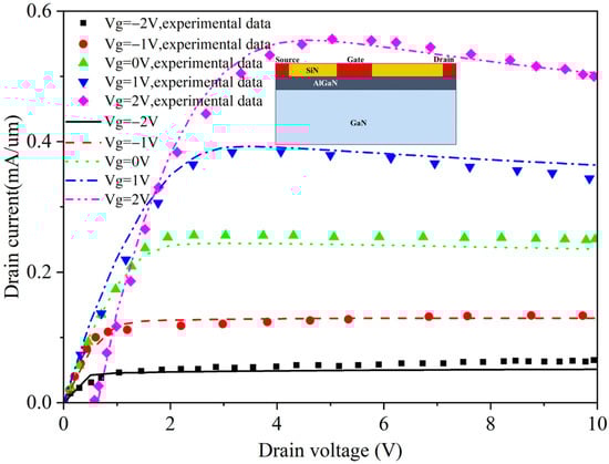
Figure 1.
Comparison of simulated drain currents with experimental drain currents. The experimental data in the figure comes from Ref. [31].
To study the Gunn oscillation effect in the channel of GaN HEMT devices, a sandwich structure GaN HEMT device model with field plate structure is proposed in Figure 2a. This structure is commonly used to suppress the peak electric field in the channel, thereby improving the breakdown characteristics of HEMT devices. The bottom is a 2-um thick GaN buffer layer, which forms a heterojunction with a 25-nm thick unintentionally doped Al0.2Ga0.8N barrier layer, and the top is a 65-nm thick SiN passivation layer. The gate length (Lg) is 300 nm, and the distances from the gate to the source (Lsg) and drain (Lgd) are 500 nm and 1200 nm, respectively. Compared to the conventional HEMT (Figure 2b), the field plate HEMT has an additional field plate structure on the right side above the gate, of which the field plate length is Lr. The gate contact is a Schottky contact with a work function of 5.1 eV; source contact and drain contact are ohmic contact.
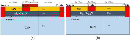
Figure 2.
GaN HEMT structural model: (a) field plate HEMT; (b) conventional HEMT.
For the transient simulations, the applied gate voltage is set to 2 V, and the drain voltage increases from 0 V to 20 V, while the field plate length of the field plate HEMT is set to 300 nm. The resulting drain current curve changes as shown in Figure 3. In the drain current curve of traditional HEMT devices, no significant oscillation current is observed. However, when the drain bias voltage reaches a certain range, there is a significant oscillation in the drain current curve of the field plate HEMT device. When the Vds is small, the electric field does not enter the NDM region. As the Vds increases, the electric field gradually increases until it exceeds the NDM region. In both cases, electrons are unable to accumulate to form electron domains, so the oscillations are not observed when the Vds is too small or too large. This indicates that compared to traditional HEMT device structures, the field plate structure can promote the generation of Gunn oscillation current by modulating the channel electric field of HEMT devices. For the GaN HEMT model with a field plate structure, the field plate, insulation layer and semiconductor constitute the MIS structure. The gate voltage causes the MIS structure to be in a depleted state, and the depletion region is connected with the depletion region of the Schottky junction of the gate electrode. In the AlGaN depletion layer, part of the electric field lines that originally ended at the gate are changed to end at the field plate. This is equivalent to introducing an additional fixed negative charge to the depletion layer surface below the field plate, which generates an electric field parallel to the surface in addition to an electric field perpendicular to the surface. At the edge of the field plate, the rightward transverse electric field generated by all negative charges is mutually reinforcing, resulting in a peak electric field at the edge of the field plate. Therefore, there is a high electric field intensity in the channel below the field plate. In this region, the electric field enters the NDM region, and the larger the electric field, the lower is the average drift velocity of electrons. Due to the difference in the velocity of electrons inside and outside this region, electrons accumulate to form electron domains, which generate oscillating currents.
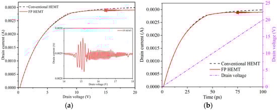
Figure 3.
Comparison of drain currents. (a) Curve of drain current variation with drain voltage; (b) drain current and voltage curve with time.
To investigate the modulation effect of the field plate on the channel electric field of the HEMT device, the channel electric field distribution is recorded as in Figure 4. Here, the applied gate voltage is set to 2 V, the drain voltage is set to 16 V, and the field plate length of the field plate HEMT is set to 300 nm. The time interval of extracting the channel electric field distribution is 0.1 ps. It is found in Figure 4a that the peak electric field intensity of conventional GaN HEMT is as high as 1.28 × 10⁶ V/cm. It can be seen in Figure 4b that when the length of the gate field plate Lr is 300 nm, the peak electric field intensity of the gate near the drain end is 1.15 × 10⁶ V/cm. In Figure 4a, except for the strong electric field in the channel region corresponding to the gate electrode, the electric field intensity in other regions of the channel is very low, and the distribution is also very uniform. When a bias voltage is applied to the drain, a peak electric field is generated near the drain edge under the gate, but it is too narrow to satisfy the conditions for domain formation due to the short drift time. The electric field distribution remains unchanged. Therefore, for conventional HEMT devices, the I–V characteristic curve shows a relatively smooth curve form, and no current oscillation phenomenon is observed, as shown in Figure 3. Due to the connection between the field plate and the gate, the field plate has a potential similar to that of the gate, which can modulate the local electric field under the gate. In Figure 4b, the field plate weakens the peak of the peak electric field below the gate, and introduces a new peak electric field at the channel below the edge of the field plate. The introduction of a new peak electric field broadens the high electric field region in the channel of the HEMT device, making the area that can enter the NDM region more extensive, and electrons can accumulate to form electron domains. The length of the negative differential mobility region is sufficient for the electron domains to grow and mature until the domain drift reaches a steep drop in field strength after the second peak value, and the domains are depleted rapidly. This is the termination region of the Gunn domain for this device, and the dual-field peak structure of the field plate (FP) HEMT can induce spatial charge disturbances at each peak, potentially serving as nucleation zones for the electron domains. The oscillation mode of multi-domain oscillations at dual nucleation points can significantly enhance the oscillation frequency of the current. Moreover, by varying the gate bias, the two peaks can be controlled to be within or outside the negative differential mobility (NDM) region, thus regulating the number of nucleation points and altering the oscillation frequency. Under the same applied voltage, the peak value of the channel electric field at the gate edge of the HEMT with the field plate decreases, and a second peak appears near the drain electrode at the edge of the field plate, increasing the coverage area of the electric field curve. The results are consistent with those of [33]. In addition, the depletion layer is formed in the AlGaN barrier layer by the field plate, which alleviates the bending degree of the depletion layer at the gate edge and reduces the peak electric field at the gate edge, thus affecting the distribution of the channel electron density.
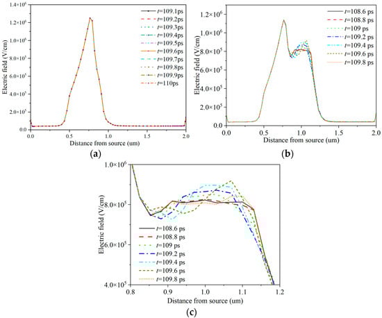
Figure 4.
Transient distribution of the electric field in the channel: (a) conventional HEMT; (b) FP HEMT; (c) corresponding partial view of (b).
The structure parameters of field plate HEMT devices remain unchanged, and the influence of changing the field plate length Lr on the Gunn oscillation effect is considered. The resulting drain current is described in Figure 5. Here, the gate applied voltage is set to 2 V, and the range of the drain voltage is set to 0~30 V. It can be seen from Figure 5 that within a certain range, with the increase of the Lr, the drain voltage range can make the current oscillation increase. Figure 6 shows electric field and electron concentration distributions at the channel of the GaN HEMT with different field plate lengths at 100 ps. At the position of 0.7 um, corresponding to the edge position of gate electrode near the leakage electrode of the GaN HEMT device, the channel electric field intensity decreases rapidly under the action of the gate field plate. The distribution of electric field along the channel direction also varies significantly depending on the length of the gate field plate. With the increase of gate field plate length Lr, the peak value of the secondary electric field increases gradually, but the peak and valley of the channel electric field near the edge of the gate electrode decrease continuously. In addition, the positions of electron domains generated in the channel are also different. This is because different gate field plate structures have different regulatory effects on the channel electric field. This further widens the high electric field region where the device can enter the negative differential mobility region, extending the length of the region where electron accumulation can occur, leading to an increase in the crossing distance of the electron domains. To illustrate the position of electron domain formation, the distributions of channel electron concentration at different times at Lr = 0.2 um are described in Figure 7 which shows the obvious resonance phenomenon under the Lr = 0.2 um field plate. Therefore, the distribution of electrons along the channel direction corresponds to the distribution of the electric field. Figure 8a illustrates the evolution of drain current under the application of drain voltage capable of generating a stable oscillating current in devices of different field plate lengths. Figure 8b shows the frequency characteristics of drain current after FFT transformation. As the length of the gate field plate Lr increases, the length of the transit region increases and the fundamental frequency and second harmonic frequency generated by the device continuously decrease. The increase in the length of the gate field plate will lead to an increase in the parasitic capacitance Cgs and Cgd of GaN HEMT devices, ultimately resulting in a weakening of the frequency characteristics. However, it is also not possible to use a gate field plate structure that is too short for regulation. This is because a short field plate forms a narrow region of high electric field in the channel, and it is too narrow to form electron domains.
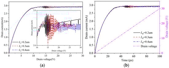
Figure 5.
Drain current at different Lr. (a) Curve of drain current variation with drain voltage; (b) drain current and voltage curve with time.
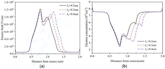
Figure 6.
Electric field and electron concentration distribution at the channel: (a) Channel electric field distribution; (b) electron concentration distribution at different Lr.
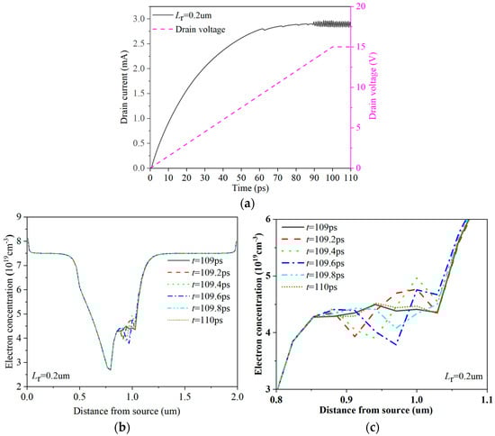
Figure 7.
Distributions of channel electron concentration at different times at Lr = 0.2 um. (a) The I−t curve and the voltage corresponding to the time; (b) channel electron concentration distribution at different times; (c) local distribution map of channel electron concentration at different times.
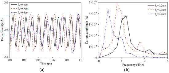
Figure 8.
Drain current characteristics: (a) evolution of drain current; (b) frequency characteristics.
By applying voltage at the gate extreme to modulate the electric field distribution in the channel below the gate, the frequency of the oscillation current can be adjusted. Drain current characteristics under different gate voltages Vg are shown in Figure 9, where the field plate length of the field plate HEMT is set to 300 nm. As the gate voltage increases, drain current also increases. The reason is that the increase of Vg leads to an increase in the depth of potential wells in the AlGaN/GaN heterojunction, thereby affecting the density of two-dimensional electron gases and subsequently affecting the current. In addition, as the gate voltage Vg increases, the drain source voltage Vds required for current oscillation also increases. This is because the height of the Schottky gate barrier decreases with increasing Vgs, resulting in a decrease in the electric field in the channel below the gate. Therefore, a larger drain source voltage Vds is required to elevate the electric field to the negative differential mobility region, thereby generating electron domains.
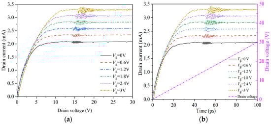
Figure 9.
Drain current characteristics under different gate voltages. (a) Curve of drain current variation with drain voltage; (b) drain current and voltage curve with time.
Figure 10 shows the transient distribution of the channel electric field Ex under different gate voltages Vg, where the drain-source bias Vds is set to 16 V and the field plate length of the field plate HEMT is set to 300 nm. With increasing gate voltage, there is a noticeable change in the electron domain crossover distance. This can be explained by the fact that as the applied bias increases, more electrons fill the channel, resulting in more electron transitions. Consequently, the electron domains become larger. When they pass through the region where the transverse electric field decreases due to the field plate, the electron domains require a longer time to neutralize. The increase in bias also amplifies the electric field on the side of the field plate, expanding the negative differential mobility region. Therefore, the distance covered by the electronic domain has been extended. Figure 11 shows the frequency characteristics of drain current under different gate voltage Vg at Vds = 16 V and Lr = 300 nm. The increase in the electron domain crossover distance d will lead to a decrease in frequency.
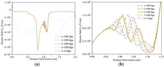
Figure 10.
Transient distribution of channel electric field under different gate voltages Vg: (a) Vg = 0 V; (b) partial enlarged view of (a); (c) Vg = 0.75 V; (d) partial enlarged view of (c).
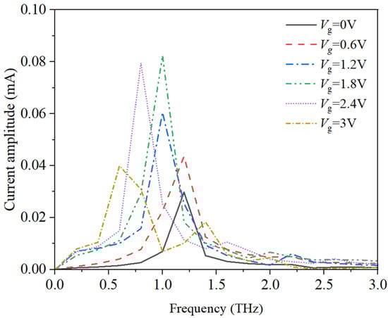
Figure 11.
Frequency characteristics of drain current at different gate voltages.
The related problems caused by defects in GaN-based HEMTs have always been an important factor limiting their development, and the trap effect caused by defects has a serious impact on the performance of devices [34,35,36]. In actual HEMT devices, the presence of defects can mask the small oscillating currents, making them difficult to measure. Figure 12 illustrates the impact of trap effects on the oscillating current of HEMT devices. As the trap concentration Ntrap increases, the oscillation phenomenon begins to advance accordingly. When the trap concentration increases to a certain extent, the current oscillation phenomenon will gradually disappear. The acceptor trap in the GaN buffer layer will trap electrons and reduce the two-dimensional electron gas concentration, so that the output current is reduced, and the electron domain cannot be formed. Because the thickness of the buffer layer is large, the trap has the obvious effect of trapping electrons, so the trap in the buffer layer is also the main cause of the current collapse effect.
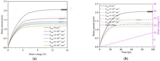
Figure 12.
Output current at different trap concentrations. (a) Curve of drain current variation with drain voltage; (b) Drain current and voltage curve with time.
Figure 13 illustrates the effect of different SiN passivation layer thicknesses (hSiN) on the transient drain current for the GaN-based HEMT model with the field plate structure. Here, Vg is set to 2 V and the field plate length Lr is set to 300 nm. With the passage of time, with the smaller the thickness of the passivation layer hSiN, the first current oscillation occurs. When the drain voltage is stabilized, there is a stable current oscillation. Therefore, the regulatory effect of the field plate structure on the electric field distribution in the channel below the gate is also greatly influenced by the SiN passivation layer. The thickness of the passivation layer in the conventional field-plate HEMT structure is usually more than 500 nm, and it is difficult for electrons to form stable electron domains. Reducing the thickness of the passivation layer within a certain range can indeed disperse the electric field under the gate, reduce the peak value, and improve the breakdown voltage. However, an excessively thin passivation layer can cause the peak electric field near the drain side of the channel below the field plate to be greater than the peak electric field strength on the gate drain side, thereby reducing the voltage resistance performance and making the device more susceptible to breakdown. Therefore, with the increase of the passivation layer thickness hSiN, the modulation effect of the field plate on electric field distribution in the lower channel is also weakened, resulting in the hysteresis of the current oscillation phenomenon.
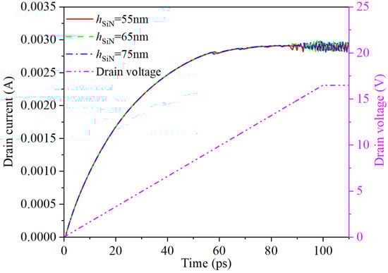
Figure 13.
Transient drain current under different SiN passivation layer thicknesses (hSiN).
Figure 14 describes the electric field distribution in the channels of HEMT devices and the current frequency characteristics under different SiN passivation layer thicknesses hSiN. For the current frequency characteristics, the current values come from drain current values within the time period of 109 ps–110 ps in Figure 13. It can be seen from the figure that the modulation ability of the field plate on the channel electric field distribution weakens with the increase of the passivation layer hSiN. The peak electric field near the edge of the drain side of the channel below the field plate decreases, the electron domain becomes smaller, and the transition distance of the electron domain decreases. For Figure 14g, it is obvious that increasing the thickness of the passivation layer within a certain range can increase the frequency and amplitude of the current oscillation, but this increase becomes relatively weak when reaching a certain value. Because the thickness of the passivation layer will affect the modulation ability of the field plate, it is important to choose a reasonable thickness.
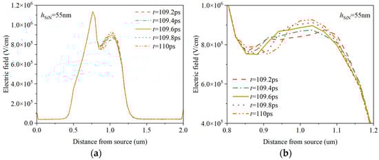
Figure 14.
Channel electric field distributions and current frequency characteristics under different SiN passivation layer thicknesses hSiN. (a) hSiN = 55 nm; (b) partial enlarged view of (a); (c) hSiN = 65 nm; (d) partial enlarged view of (c); (e) hSiN = 75 nm; (f) partial enlarged view of (e); (g) current frequency characteristics.
4. Conclusions
In this paper, a GaN-based HEMT model with a field plate structure was proposed to achieve stable, reliable, and useful terahertz wave output. The hydrodynamic physical model was established and solved by the finite element method. The suitable field plate structure can modulate the distribution of the channel electric field below the gate, and promote the electric field to enter the negative differential mobility region. Within a certain range, a shorter gate field plate length helps to increase the current oscillation frequency of the device. When the trap concentration increases a certain extent, the current oscillation phenomenon will gradually disappear. This study provides a theoretical basis for semiconductor solid-state devices to realize terahertz band radiation.
Author Contributions
Conceptualization, R.Y.; methodology, R.Y.; software, R.Y.; validation, R.Y. and J.W.; formal analysis, R.Y.; investigation, R.Y. and J.W.; data curation, R.Y. and J.W.; writing—original draft preparation, R.Y.; writing—review and editing, L.W.; visualization, R.Y. and J.W.; supervision, L.W.; project administration, L.W.; funding acquisition, L.W. All authors have read and agreed to the published version of the manuscript.
Funding
This research was funded by the National Natural Science Foundation of China, grant number 62301449, the Natural Science Foundation of Sichuan Province, China, grant number 24NSFSC3981, the Electromagnetic Technology and Engineering Key Laboratory of Nanchong City, grant number NCKL202005, and the Fundamental Research Funds of China West Normal University, grant number 22kE005 and 23kc003.
Data Availability Statement
The original contributions presented in the study are included in the article, further inquiries can be directed to the corresponding author.
Conflicts of Interest
The authors declare no conflicts of interest.
References
- Bradley, F.; Zhang, X.C. Materials for terahertz science and technology. Nat. Mater. 2002, 1, 26–33. [Google Scholar]
- Peng, L.; Zhang, Z.H.; Zhang, G. Efficient GaN-on-Si power amplifier design using analytical and numerical optimization methods for 24–30 GHz 5G applications. Electronics 2023, 12, 1750. [Google Scholar] [CrossRef]
- Yu, D.Y.; Yang, H.R.; Li, H.G. Analysis and processing of noise in weak terahertz signal detection system. J. Appl. Opt. 2012, 33, 1101–1104. [Google Scholar]
- Zhou, Y.L.; Qin, J.; Xie, Z.J.; Wang, H. Performance enhancement for AlGaN/GaN HEMTs with dual discrete field-plate. Solid-State Electron. 2023, 200, 108571. [Google Scholar] [CrossRef]
- Patiño-Gómez, M.; Ortega-González, F.J. High-efficiency GaN-Based power amplifiers for envelope nonlinearities’ mitigation in VHF wideband polar-mode transmitters. Electronics 2023, 12, 3866. [Google Scholar] [CrossRef]
- Higashiwaki, M.; Onojima, N.; Matsui, T.; Mimura, T. Effects of SiN passivation by catalytic chemical vapor deposition on electrical properties of AlGaN/GaN heterostructure field-effect transistors. J. Appl. Phys. 2006, 100, 033714. [Google Scholar] [CrossRef]
- Zybura, M.F.; Jones, S.H.; Tait, G.B.; Tait, G.B. 100–300 GHz Gunn oscillator simulation through harmonic balance circuit analysis linked to a hydrodynamic device simulator. IEEE Microw. Guided Wave Lett. 1994, 4, 282–284. [Google Scholar] [CrossRef]
- Khalid, A.; Pilgrim, N.J.; Dunn, G.M.; Holland, M.C.; Stanley, C.R.; Thayne, I.G.; Cumming, D.R.S. A planar Gunn diode operating above 100 GHz. IEEE Electron Device Lett. 2007, 28, 10. [Google Scholar] [CrossRef]
- Pérez, S.; González, T.; Pardo, D.; Mateos, J. Terahertz Gunn-like oscillations in InGaAs/InAlAs planar diodes. J. Appl. Phys. 2008, 103, 094516. [Google Scholar] [CrossRef]
- Xu, K.Y.; Wang, G.; Song, A.M. Gunn oscillations in a self-switching nanodiode. Appl. Phys. Lett. 2008, 93, 233506. [Google Scholar] [CrossRef]
- Íñiguez-de-la-Torre, A.; Íñiguez-de-la-Torre, I.; Mateos, J.; González, T.; Sangaré, P.; Faucher, M.; Grimbert, B.; Brandli, V.; Ducournau, G.; Gaquière, C. Searching for THz Gunn oscillations in GaN planar nanodiodes. J. Appl. Phys. 2012, 111, 113705. [Google Scholar] [CrossRef]
- Wang, Y.; Yang, L.A.; Mao, W.; Long, S.; Hao, Y. Modulation of multidomain in AlGaN/GaN HEMT-like planar Gunn diode. IEEE Trans. Electron Devices 2013, 60, 1600–1606. [Google Scholar] [CrossRef]
- Pan, J.T.; Wang, Y.; Xu, K.Y.; Xiong, J.W.; Tang, Z.L. Tunable Gunn oscillations in a top-gated planar nanodevice. Solid State Commun. 2018, 271, 85–88. [Google Scholar] [CrossRef]
- Zhao, H.L.; Yang, L.A.; Zou, H.; Ma, X.H.; Hao, Y. Enhancement of negative differential mobility effect in recessed barrier layer Al-GaN/GaN HEMT for terahertz applications. IEEE Trans. Electron Devices 2019, 66, 1236–1242. [Google Scholar] [CrossRef]
- Zou, H.; Yang, L.A.; Ma, X.H.; Hao, Y. Effects of notch structures on DC and RF performances of AlGaN/GaN high electron mobility transistors. Chin. Phys. B 2021, 30, 040502. [Google Scholar] [CrossRef]
- Basumatary, B.; Maity, S.; Muchahary, D. Improvement of drain current of AlGaN/GaN-HEMT through the modification of negative differential conductance (NDC), current collapse, self-heating and optimization of double hetero structure. Superlattices Microstruct. 2016, 97, 606–616. [Google Scholar] [CrossRef]
- Binder, A.T.; Yuan, J.S.; Krishnan, B.; Shea, P.M.; Yeh, W.K. Trap induced negative differential conductance and back-gated charge redistribution in AlGaN/GaN power devices. Microelectron. Reliab. 2019, 102, 113495. [Google Scholar] [CrossRef]
- Delagebeaudeuf, D.; Linh, N.T. Metal-(n) AlGaAs-GaAs two-dimensional electron gas FET. IEEE Trans. Electron Devices 1982, 29, 955–960. [Google Scholar] [CrossRef]
- An, Y.; Ren, K.; Yin, L.Q.; Zhang, J.H. Modeling on monolithic integration structure of AlGaN/InGaN/GaN high electron mobility transistors and LEDs: 2DEG density and radiative recombination. Electronics 2023, 12, 1087. [Google Scholar] [CrossRef]
- Smorchkova, I.P.; Elsass, C.R.; Ibbetson, J.P.; Vetury, R.; Heying, B.; Fini, P.; Haus, E.; DenBaars, S.P.; Speck, J.S.; Mishra, U.K. Polariza-tion-induced charge and electron mobility in AlGaN/GaN heterostructures grown by plasma-assisted molecular-beam epitaxy. J. Appl. Phys. 1999, 86, 4520–4526. [Google Scholar] [CrossRef]
- Ambacher, O.; Foutz, B. Two-dimensional electron gases induced by spontaneous and piezoelectric polarization charges in N- and Ga-face AlGaN/GaN heterostructures. J. Appl. Phys. 1999, 85, 3222–3233. [Google Scholar] [CrossRef]
- Mo, J.H.; Cai, S.J. Summarize for the investigation of the filed-plate structure in GaN-based HEMT. Semicond. Technol. 2006, 31, 402–405. [Google Scholar]
- Stratton, R. Semiconductor current-flow equations (diffusion and degeneracy). IEEE Trans. Electron Devices 1972, 19, 1288–1292. [Google Scholar] [CrossRef]
- Nuo, M.Q.; Wei, J.; Wang, M.J.; Yang, J.J.; Wu, Y.L.; Hao, Y.L.; Shen, B. Gate/drain coupled barrier lowering effect and negative threshold voltage shift in schottky-type p-GaN gate HEMT. IEEE Trans. Electron Devices 2022, 69, 3630–3635. [Google Scholar] [CrossRef]
- Liao, H.; Zheng, Z.Y.; Chen, T.; Zhang, L.; Cheng, Y.; Feng, S.R.; Ng, Y.H.; Chen, L.; Yuan, L.; Chen, K.J. Normally-off p-GaN gate double-channel HEMT with suppressed hot-electron-induced dynamic on-resistance degradation. IEEE Electron Device Lett. 2022, 43, 1424–1427. [Google Scholar] [CrossRef]
- Alekseev, E.; Pavlidis, D. Large-signal microwave performance of GaN-based NDR diode oscillators. Solid State Electron. 2000, 44, 941–947. [Google Scholar] [CrossRef]
- Zybura, M.F.; Jones, S.H.; Tait, G.; Duva, J.M. Efficient computer aided design of GaAs and InP millimeter wave transferred electron devices including detailed thermal analysis. Solid-State Electron. 1995, 38, 873–880. [Google Scholar] [CrossRef]
- Farahmand, M.; Garetto, C.; Bellotti, E.; Brennan, K.F.; Goano, M.; Ghillino, E.; Ghione, G.; Albrecht, J.D.; Ruden, P.P. Monte Carlo simulation of electron transport in the III-nitride wurtzite phase materials system: Binaries and ternaries. IEEE Trans. Electron Devices 2001, 48, 535–542. [Google Scholar] [CrossRef]
- Sun, S.C.; Plummer, J.D. Electron mobility in inversion and accumulation layers on thermally oxidized silicon surfaces. IEEE J. Solid-State Circ. 1980, 15, 1497–1508. [Google Scholar] [CrossRef]
- Wang, S.L.; Dou, Y.L.; Liu, H.X.; Lin, Z.Y.; Zhang, H.L. Electron momentum and energy relaxation times in Wurtzite GaN, InN and AlN: A Monte Carlo study. J. Electron. Mater. 2017, 47, 1560–1568. [Google Scholar] [CrossRef]
- Maeda, T.; Narita, T.; Ueda, H.; Kanechika, M.; Uesugi, T.; Kachi, T.; Kimoto, T.; Horita, M.; Suda, J. Shockley–Read–Hall lifetime in homoepitaxial p-GaN extracted from recombination current in GaN p–n+ junction diodes. Jpn. J. Appl. Phys. 2019, 58, SCCB14. [Google Scholar] [CrossRef]
- Zou, H.; Yang, L.A.; Ma, X.H.; Hao, Y. The dual-suppression of peak electric field in AlGaN/GaN HEMT with sandwich structure. Superlattices Microstruct. 2021, 152, 106843. [Google Scholar] [CrossRef]
- Tang, X.; Rousseau, M.; Dalle, C.; De Jaeger, J.C. Physical analysis of thermal effects on the optimization of GaN Gunn diodes. Appl. Phys. Lett. 2009, 95, 142102. [Google Scholar] [CrossRef]
- Zheng, X.; Feng, S.W.; Zhang, Y.M.; He, X.; Wang, Y. A new differential amplitude spectrum for analyzing the trapping effect in GaN HEMTs based on the drain current transient. IEEE Trans. Electron Devices 2017, 64, 1498–1504. [Google Scholar] [CrossRef]
- Makaram, P.; Joh, J.; Del Alamo, J.A.; Palacios, T.; Thompson, C.V. Evolution of structural defects associated with electrical degradation in AlGaN/GaN high electron mobility transistors. Appl. Phys. Lett. 2010, 96, 233509. [Google Scholar] [CrossRef]
- Chini, A.; Soci, F.; Meneghini, M.; Meneghesso, G.; Zanoni, E. Deep levels characterization in GaN HEMTs—part II: Experimental and numerical evaluation of self-heating effects on the extraction of traps activation energy. IEEE Trans. Electron Devices 2013, 60, 3176–3182. [Google Scholar] [CrossRef]
Disclaimer/Publisher’s Note: The statements, opinions and data contained in all publications are solely those of the individual author(s) and contributor(s) and not of MDPI and/or the editor(s). MDPI and/or the editor(s) disclaim responsibility for any injury to people or property resulting from any ideas, methods, instructions or products referred to in the content. |
© 2024 by the authors. Licensee MDPI, Basel, Switzerland. This article is an open access article distributed under the terms and conditions of the Creative Commons Attribution (CC BY) license (https://creativecommons.org/licenses/by/4.0/).