Article

A Broadband Three-Way Series Doherty Power Amplifier with Deep Power Back-Off Efficiency Enhancement for 5G Application

by
Xianfeng Que
1,
Jun Li
2 and
Yanjie Wang
2,*
1
School of Electronic and Information Engineering, South China University of Technology, Guangzhou 510641, China
2
School of Microelectronics, South China University of Technology, Guangzhou 510641, China
*
Author to whom correspondence should be addressed.
Electronics 2024, 13(10), 1882; https://doi.org/10.3390/electronics13101882
Submission received: 4 April 2024 / Revised: 7 May 2024 / Accepted: 9 May 2024 / Published: 11 May 2024

Abstract

:
This article presents a new broadband three-way series Doherty power amplifier (DPA) topology, which enables a broadband output power back-off (OBO) efficiency enhancement of up to 10 dB or higher. The proposed DPA topology achieves Doherty load modulation and three-way power combining through a transformer, which requires only a low coupling factor, thus facilitating its implementation in double-sided PCBs or monolithic microwave integrated circuit (MMIC) processes. The design equations for the proposed DPA topology are proposed and analyzed in detail. A proof-of-concept PA at the 2.1–2.8 GHz band using commercial GaN transistors was designed and fabricated to validate the proposed concept. Within the operating frequency band, it achieves a saturated output power ( P sat ) of 44.5–46.5 dBm with a peak drain efficiency (DE) of 60–72%, and 43–52% DE at 10 dB OBO. Moreover, under a 20 MHz long-term evolution (LTE)-modulated signal, the PA demonstrates a 36.8–37.5 dBm average output power ( P avg ) and 47–53% average drain efficiency ( DE avg ). Notably, the adjacent channel leakage ratio (ACLR) is as low as −35–−28.2 dBc without any digital predistortion (DPD).

1. Introduction

Demands for elevated data rates and expanded capacity mandate the incorporation of intricate signal modulation techniques in fifth-generation (5G) communication systems, including high-order quadrature amplitude modulation (QAM), massive multiple-input multiple-output (MIMO), and orthogonal frequency-division multiplexing (OFDM) [1,2]. However, these techniques pose challenges, such as a high peak-to-average power ratio (PAPR) of up to 9–12 dB, coupled with the necessity for a high degree of linearity in communication systems [3,4,5]. Consequently, power amplifiers (PAs) must operate at deep output power back-off (OBO), resulting in a diminished average efficiency [6]. Given that PAs are typically the most power-consuming components in wireless communication systems, their inefficiency engenders significant concerns such as constrained battery life and heightened heat dissipation [7]. This underscores the pressing need to augment the efficiency of PAs operating at deep OBO.
The Doherty power amplifier (DPA) is the most widely used architecture for improving the OBO efficiency of PAs due to its intrinsic linearity and low baseband overhead [8,9,10,11,12,13,14,15,16,17,18,19,20,21,22,23]. A DPA typically comprises a Main PA and an Auxiliary PA, with its OBO efficiency enhanced through active load modulation between these two sub-PAs. At low power levels with OBO above 6 dB, the Auxiliary PA is off, while the Main PA has a high load impedance and maintains a high efficiency owing to the large drain voltage swing. At high power levels, the Auxiliary PA turns on, modulating the load impedance of the Main PA from high impedance to optimal impedance ( R opt ), thereby ensuring maximum output power.
DPA comprises two fundamental topologies: parallel and series, as depicted in Figure 1 [8]. In the parallel topology, the Main PA is connected in parallel with the Auxiliary PA via a λ / 4 transmission line (TL), resulting in a load impedance of R opt / 2 . In the series topology, the Auxiliary PA is connected in series with the Main PA through a λ / 4 TL and a transformer, resulting in a load impedance of 2   ×   R opt .
The parallel topology has been the prevalent choice for reported DPAs due to its ease of implementation [15,16,17,18,19]. Nevertheless, a two-way parallel DPA is restricted to providing efficiency improvements within 6 dB OBO, which is insufficient for the 5G NR waveform. To extend the OBO range, N-way (where N = 3 or 4) parallel DPAs have been developed, achieving a deep OBO range of up to 9–12 dB [20,21,22,23]. However, N-way parallel DPAs typically have a larger impedance transformation ratio (ITR) due to the need for impedance matching between R opt / N and 50 Ω at the combining node, resulting in a reduced bandwidth and efficiency, as well as significant area overhead [9,20]. This issue becomes more pronounced in high-power PA designs, where R opt commonly falls below 30 Ω [15].
Recently, a Doherty-like topology, known as the load-modulated balanced amplifier (LMBA), has been proposed and developed for broadband active load modulation [24,25,26,27,28,29,30]. However, LMBAs are prone to experiencing significant nonlinear gain compression during load modulation, which adversely impacts their linearity [26].
For high-power DPA designs, the series topology may offer more advantages. First, the ITR between N × R opt and 50 Ω is substantially lower than that of the parallel topology when R opt is small [9]. Second, the elimination of the λ / 4 TL after the Main PA enhances both the bandwidth and the linearity [8]. Nonetheless, while the series DPA topology has been successfully implemented in CMOS processes [8,9,10,11,12,13,14], its application in printed circuit board (PCB) or monolithic microwave integrated circuit (MMIC) processes is still rarely reported. This is primarily attributed to the constraints of these processes, which generally contain only two or three metal layers (including the ground layer), posing significant challenges in the fabrication of transformers with high coupling factors.
To address this issue, this paper presents a novel three-way series Doherty topology, which employs a transformer with a low coupling factor to achieve Doherty load modulation and efficient three-way power combining. The low-coupling transformer can be readily implemented in PCB and MMIC processes. Furthermore, by arranging the power ratio of the Main and Auxiliary PAs, this topology ensures a deep OBO efficiency enhancement with a low ITR, thus facilitating a high efficiency and a broad bandwidth. For the experimental validation, a prototype PA is designed, fabricated, and measured, showing good agreement between the simulated and measured results.

2. Analysis of Proposed Three-Way DPA

The conventional series DPA depicted in Figure 1b typically employs a single transformer for two-way power combining, providing an OBO range of 6 dB. However, the transformers utilized in such topology generally require high coupling factors exceeding 0.7 [12], which is difficult to achieve in double-sided PCB and MMIC processes [31,32]. Consequently, implementing conventional series Doherty PAs in these processes presents notable challenges.
In contrast, the novel series Doherty topology introduced in this paper contains a Main PA and two Auxiliary PAs, employing a single transformer along with two λ / 4 transmission lines (TLs) to realize three-way power combining, as depicted in Figure 2a. This topology not only enables higher output power but also extends the OBO range to 10 dB or deeper by arranging the power ratio between the Main PA and the Auxiliary PAs. Moreover, the load impedance seen by the Main PA at low input power remains constant at R L due to the connection setup of the Main PA and the load R L at opposite ends of the secondary coil, and is unaffected by the transformer’s turns ratio. Meanwhile, the impedance seen by the Auxiliary PAs is determined by both the turns ratio k and the characteristic impedance Z 0 of the λ / 4 TL. Therefore, the transformer in the proposed topology can exhibit a low coupling factor, which is advantageous for implementing this topology in PCB and MMIC processes. A detailed analysis of this topology is presented in this section.

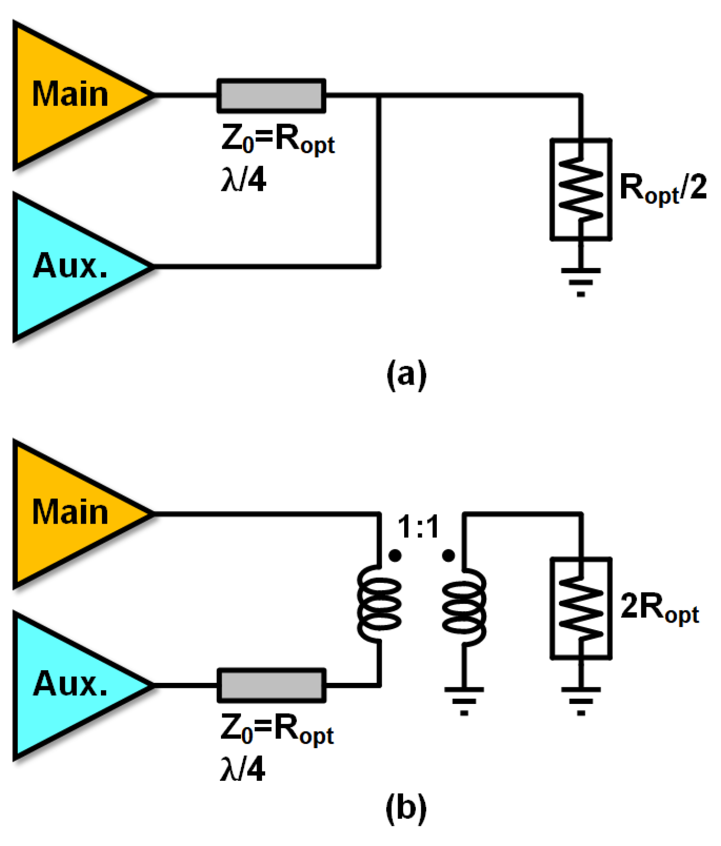
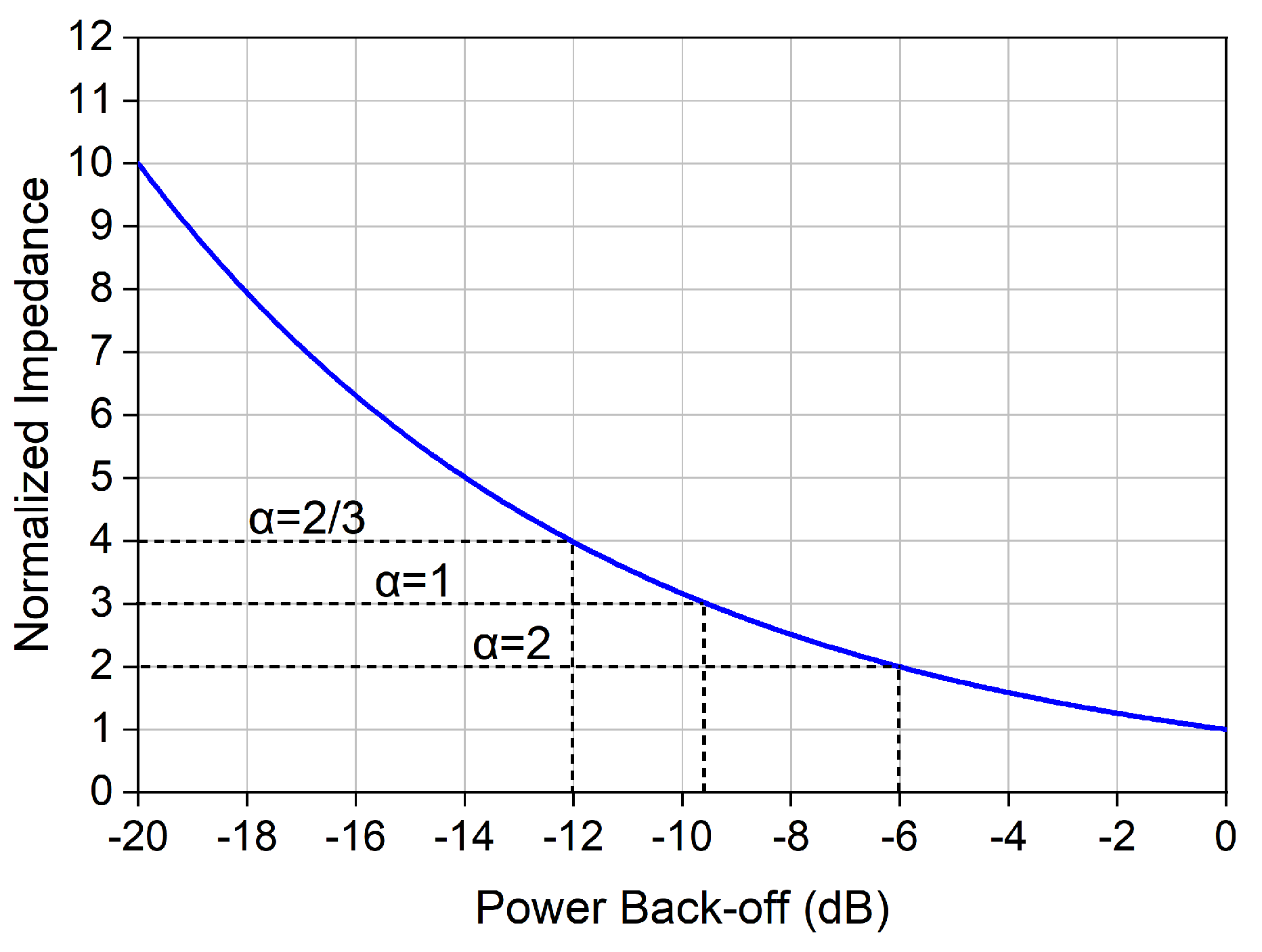
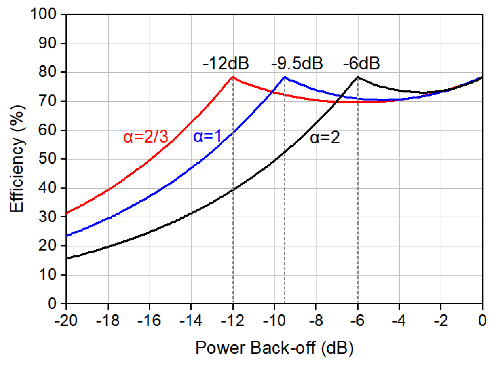
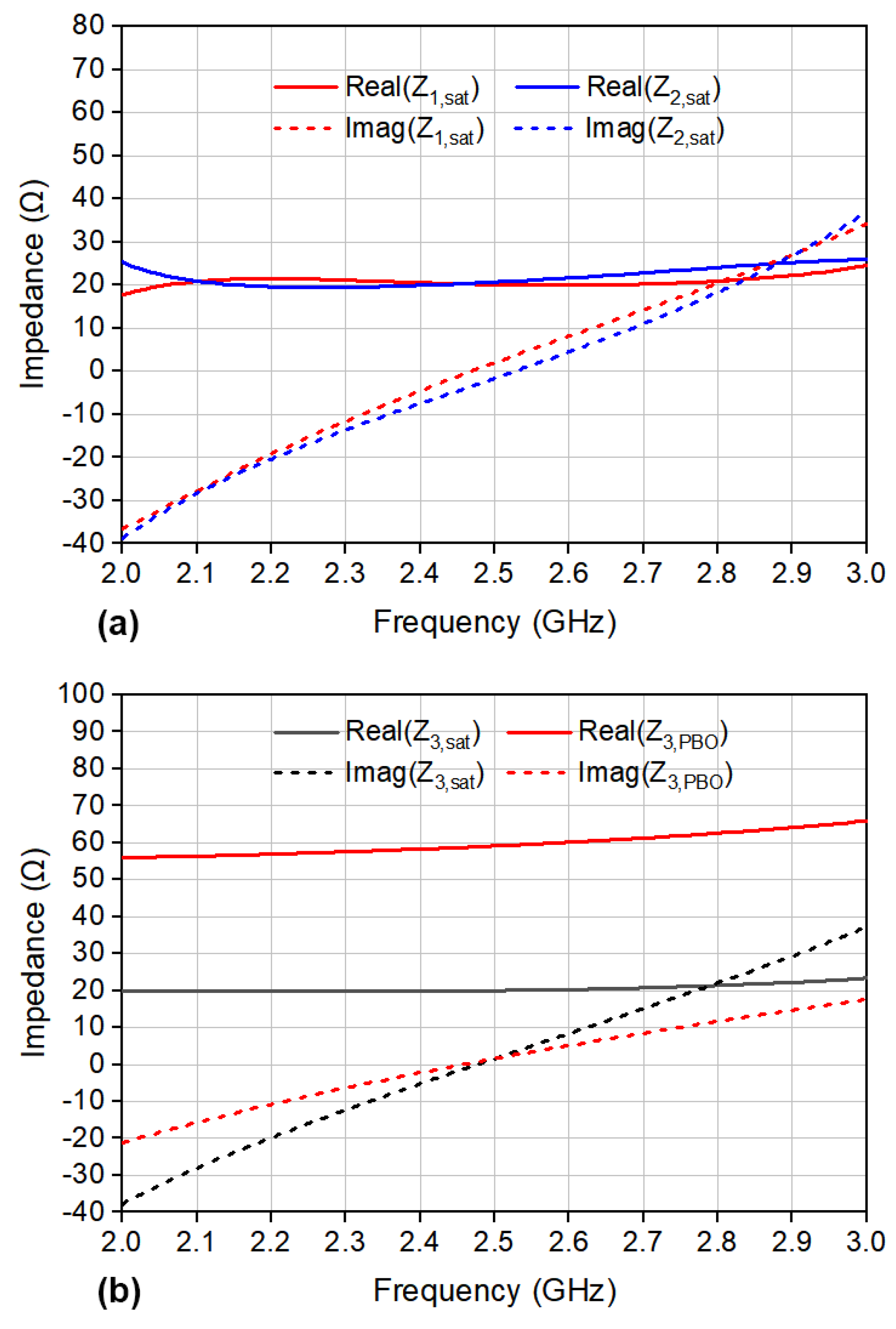
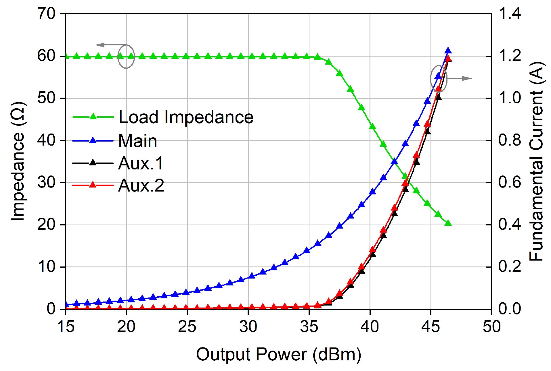
2.1. Load Modulation Analysis
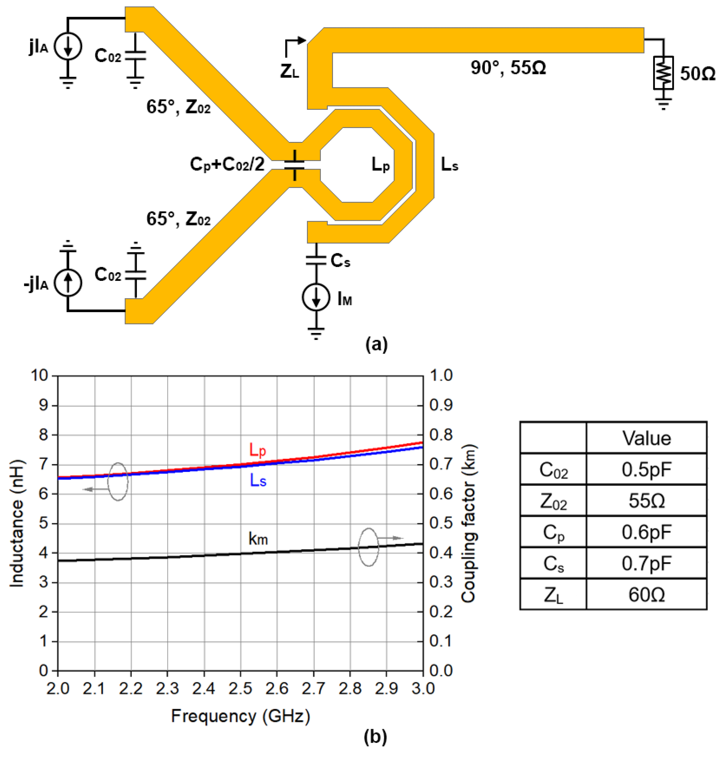
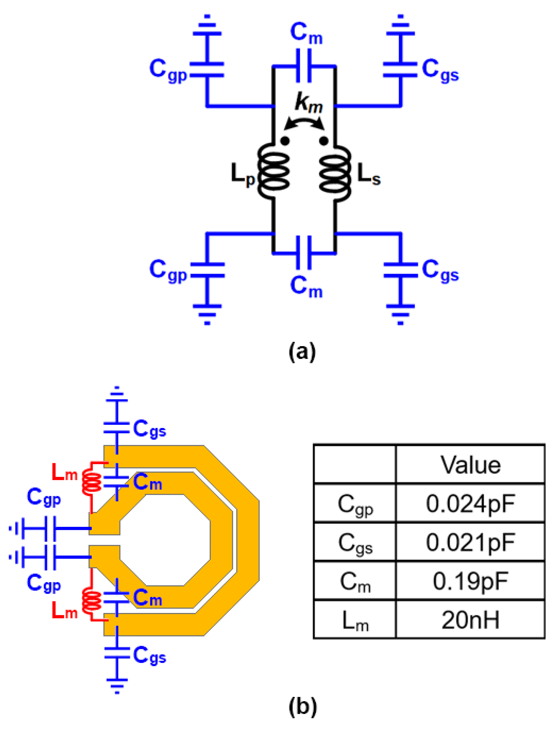
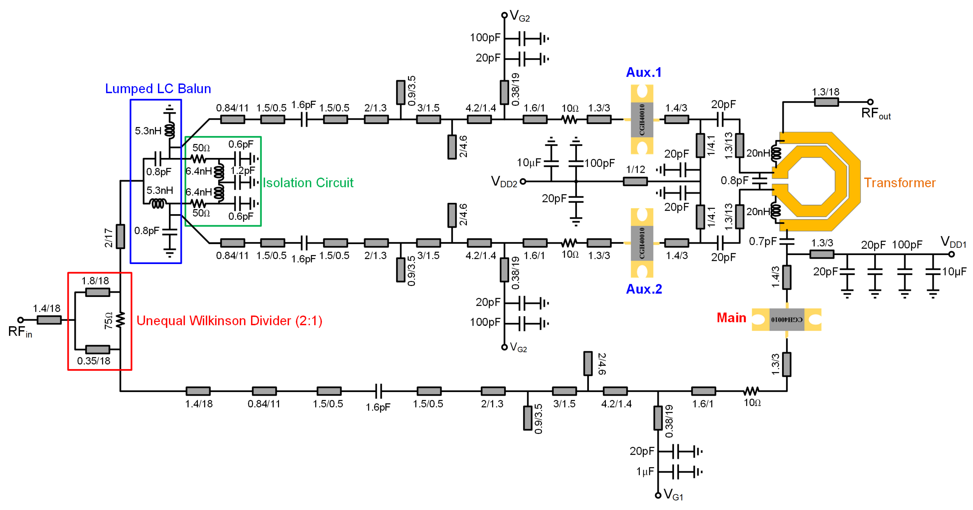
In the proposed Doherty topology, the Aux.1 and Aux.2 PAs are biased at the same gate voltage, both operating at Class-C, while the Main PA is biased at Class-AB. The active load modulation can be analyzed by examining the three-port Z-matrix (1) of the proposed topology, where ports 1 and 2 are connected to the Aux.1 PA and Aux.2 PA, respectively, and port 3 is linked to the Main PA. I 1 = j I A , I 2 = j I A , and I 3 = I M .
V 1 V 2 V 3 = 0 0 j k Z 0 0 0 j k Z 0 j k Z 0 j k Z 0 R L I 1 I 2 I 3
Z 1 = V 1 I 1 = k Z 0 I M I A Z 2 = V 2 I 2 = k Z 0 I M I A Z 3 = V 3 I 3 = R L 2 k Z 0 I A I M
It is indicated in (2) that the two Auxiliary PAs have identical load impedances, determined by the current ratio I M / I A , Z 0 , and k. At low input power, only the Main PA is active, while the Auxiliary PAs are off (i.e., I A = 0 ). Therefore, the Main PA sees a load impedance of R L , while the Auxiliary PAs see an infinite impedance (). At high input power, the Auxiliary PAs turn on and deliver currents to the output network. In this phase, the impedances of the Main PA and Auxiliary PAs decrease as I A increases. At saturation, all three sub-PAs obtain their optimal impedances, guaranteeing maximum output power.
The output powers of each sub-PA are derived from (2), expressed as follows:
P A = 1 2 I A 2 Z 1 = 1 2 k Z 0 I M I A P M = 1 2 I M 2 Z 3 = 1 2 I M 2 R L 2 k Z 0 I A I M
The calculation formula for the OBO range is given in (4) by combining (2) and (3).
O B O = P M P M + 2 P A × Z 3 R L = I M 2 R L 2 k Z 0 I A I M 2 I M 2 R L R L 2 k Z 0 I A I M + 2 k Z 0 R L I M I A
Typically, the saturated output current of a transistor exhibits direct proportionality to its saturated output power ( P s a t ) and inverse proportionality to R o p t . Let α = I M , s a t / I A , s a t . Then, the following formulas can be derived:
P A , s a t = 1 α P M , s a t
R o p t , A = α R o p t , M
Substituting (5) and (6) into (2) and (3) gives the following:
Z 1 , s a t = α k Z 0 = α R o p t , M Z 2 , s a t = α k Z 0 = α R o p t , M Z 3 , s a t = k Z 0 = R o p t , M Z 3 , l o w = R L = R o p t , M ( α + 2 ) α
O B O = α α + 2 2
Some important conclusions can be drawn from (7) and (8). First, with given values of α and R o p t , M , the load modulation behavior of the proposed Doherty topology can be determined. Second, the product of k and Z 0 equals R o p t , M . By selecting a higher Z 0 value, the k value can be reduced, thereby avoiding the need for a high-coupling transformer. Third, the OBO range is solely determined by α . A smaller α results in a deeper OBO range, and the ITR of the Main PA increases correspondingly, as shown in Figure 3. The efficiency curves for different α values are illustrated in Figure 4.
It is assumed that the three sub-PAs are of identical sizes, i.e., α = 1 . It is indicated from (7) that Z 1 , s a t = Z 2 , s a t = Z 3 , s a t = k Z 0 = R o p t and Z 3 , O B O = R L = 3 k Z 0 = 3 R o p t . If R o p t is less than 25 Ω , the ITR between R L and 50 Ω is very small, thus facilitating wide bandwidth and high efficiency. The OBO range is calculated from (8) as 9.54 dB, and the corresponding efficiency curve versus OBO is illustrated in Figure 4. The load modulations of the Main PA and Auxiliary PAs are presented in Figure 5.

2.2. Implementation

The ideal transformer in the proposed Doherty topology is realized using a pair of coupled inductors in practice, as described in Figure 2b. It is well known that the equivalent circuit of a pair of coupled inductors comprises an ideal transformer, a magnetizing inductor, and a leakage inductor. In this design, the magnetizing and leakage inductors are resonated out by adding the capacitors C p and C s , respectively. The formulas for calculating these parameters are provided in (9).
k = k m L s L p C p = 1 ( 2 π f 0 ) 2 L p C s = 1 ( 2 π f 0 ) 2 ( 1 k 2 ) L s
Furthermore, to save the circuit area, the λ / 4 TL can be replaced by a shorter TL with an electrical length of θ and a characteristic impedance of Z 02 , along with two shunt capacitors C p , as shown in Figure 2c. The calculation formulas for Z 02 , θ , and C 02 are given in (10), revealing that choosing a lower θ leads to higher values of both Z 02 and C 02 . Additionally, C 02 can be integrated with C p to obtain a capacitance value of C p + C 02 / 2 , as depicted in Figure 2d.
Z 02 = Z 0 sin θ C 02 = cos θ 2 π f 0 Z 0

3. Design Procedure

To verify the proposed theory, a prototype DPA is designed on a Rogers 4350B substrate ( ε r = 3.66 and tan δ = 0.004 ) with a thickness of 0.762 mm. The target frequency range is from 2.2 to 2.8 GHz to cover the 5G NR bands for cellular communication systems, including n40 of 2300–2400 MHz, n41 of 2496–2690 MHz, and n7 of 2620–2690 MHz. Circuit and electromagnetic (EM) simulations are conducted using the PathWave Advanced Design System (ADS) and the ANSYS High-Frequency Structure Simulator (HFSS), respectively. For ease of design, the three sub-PAs use the same packaged 10 W GaN HEMTs from MACOM (CGH40010F), i.e., α = 1 . The Main PA is biased at Class-AB with a gate voltage ( V G ) of −2.7 V and a supply voltage of 28 V, and the quiescent drain current is set at 200 mA. The Auxiliary PA is biased at Class-C with a gate voltage ( V G ) of −5.4 V, and is supplied with a slightly higher drain voltage of 32 V. This compensates for the weaker output power capability inherent in the Class-C mode [15], thereby ensuring that the P s a t of the Auxiliary PA is close to that of the Main PA. The R o p t and output capacitance ( C o u t ) of the HEMTs are extracted from a load-pull simulation, as shown in Figure 6. For maximum output power and optimal bandwidth, the load impedance is selected as 15.9 + j8.1 Ω at a center frequency of 2.5 GHz, with its conjugate value corresponding to 20 Ω R o p t in parallel with 1.6 pF C o u t .
The design of the output network is a crucial task in this work. The transformer features a uniplanar structure, with both the primary and secondary coils comprising a single turn. The width of the coils is designed to be 1 mm to guarantee adequate power-carrying capacity. According to the IPC-2221A standard [33], a 1 mm wide microstrip line carrying a current of 1.5–5.5 A experiences a temperature rise of 10–100 °C. For a 50 Ω load, the current corresponds to an output power of 112.5–1512.5 W. In this design, with a maximum output power of 46.5 dBm (i.e., 44.7 W), employing a line width of 1 mm ensures that the temperature rise remains below 10 °C. The layout of the output network is illustrated in Figure 7a. The values of L p , L s , and k m are extracted from the EM simulation results, as shown in Figure 7b. L p and L s are both approximately 7 nH, and k m is 0.4. The other parameters are subsequently calculated from (9) and displayed in Figure 7b. The physical lengths of the two TLs are 13 mm, corresponding to an electrical length of 65°, with a characteristic impedance Z 02 and an associated shunt capacitance C 02 calculated as 55 Ω and 0.54 pF, respectively, using (10). Additionally, a λ / 4 TL with a characteristic impedance of 55 Ω is positioned after the combining node, serving as a post-matching network to transform R L to 50 Ω . It is crucial to note that the ITR between R L and 50 Ω is merely 1.2 in this topology. In comparison, the parallel Doherty counterpart has a much higher ITR of 7.5.
The equivalent circuit of the ideal coupled inductor is illustrated in Figure 2b. However, practical coupled coils exhibit parasitic capacitors C m between the primary and secondary coils, as well as parasitic capacitors C g p and C g s between the coils and the ground [34], as depicted in Figure 8a. These parasitic capacitors cause deviations in the performance of the coupled inductor from the ideal model. The values of C m , C g p , and C g s in the proposed output network are extracted from the EM simulation and presented in Figure 8b. Among them, the values of C g p and C g s are relatively small and can be neglected, while the value of C m is 0.19 pF. To resonate out C m , two 20 nH packaged inductors are inserted between the primary and secondary coils, bringing the performance of the coupled coils closer to that of the ideal coupled inductors.
The three-way Doherty behavior of the output network is simulated by modeling the three sub-PAs as ideal current sources, with the results depicted in Figure 9. At the peak output power, the output network provides nearly identical impedances of approximately 20 Ω ( R o p t ) for all three sub-PAs. When both Auxiliary PAs are in the off state, the Main PA sees a load impedance of 59.2 Ω (2.96× R o p t ). The simulation results confirm that the output network achieves the required Doherty active load modulation across a wide bandwidth, attributed to its low ITR.
The input feed comprises a 2:1 unequal Wilkinson divider with an isolation resistor of 75 Ω and a lumped LC balun, splitting the input RF power to three paths with equal amplitude and proper phase difference. A lumped isolation circuit is inserted between the balanced ports of the lumped balun to enhance isolation between the two Auxiliary paths, thereby improving the circuit stability [31], as shown in Figure 10. The input matching network (IMN) is designed to maximize the bandwidth and minimize the input reflection coefficient. Given that all three sub-PAs employ identical transistors, the same IMNs are deployed for them to simplify the design process. Additionally, a 10 Ω resistor is included in the IMN to guarantee the PA’s stability.
A schematic of the entire PA design is illustrated in Figure 10, including the dimensions of the TLs and the values of the lumped components.
The post-layout electromagnetic (EM) simulation of the PA is conducted using ANSYS HFSS 2021 R2. The large-signal simulation results from 2.1 to 2.8 GHz are shown in Figure 11. The proposed PA achieves 63.9–73.1% drain efficiency (DE) at saturation, and 43–51.7% DE at 10 dB OBO. The saturated output power ( P s a t ) reaches 46.7 dBm and remains above 44.8 dBm across the entire frequency range.
To better illustrate the load modulation of the proposed PA, Figure 12 presents the simulated load impedance at the drain of the Main PA, and the output currents of the Main, Aux.1, and Aux.2 PAs versus the output power at 2.5 GHz. The output current of the Main PA increases monotonically as the input power increases, while the Aux.1 and Aux.2 PAs remain inactive at low input power and become activated around the 10 dB OBO point. With the activation of the Auxiliary PAs, the load impedance of the Main PA decreases from 59.6 Ω (2.98 ×   R o p t ) to 20.2 Ω (1.01 ×   R o p t ). At the saturation power, the three sub-PAs exhibit nearly identical output currents, delivering a maximum output power. The simulated load modulation aligns well with the values calculated using (5)–(8), verifying the accuracy of the theoretical analysis.

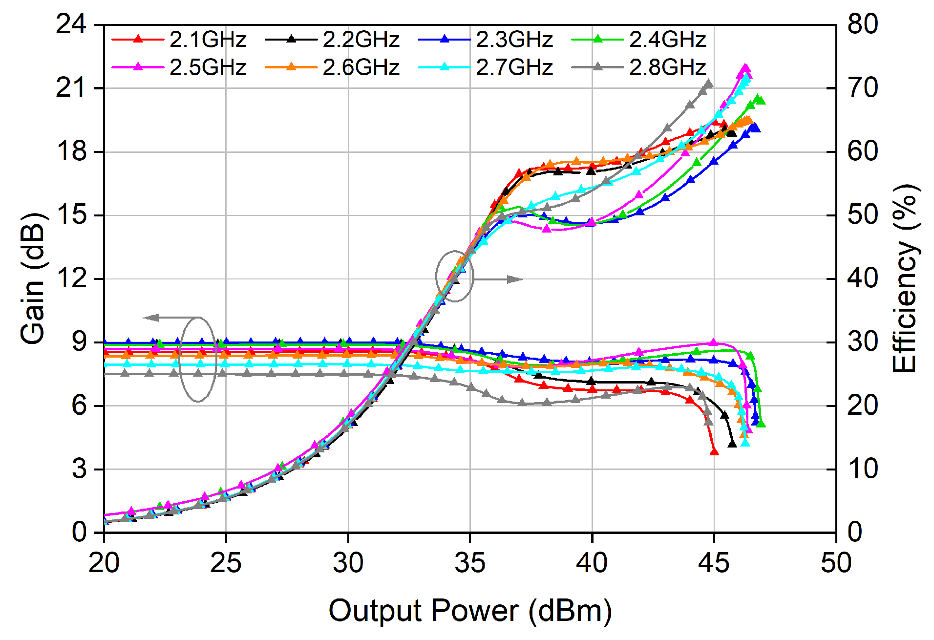
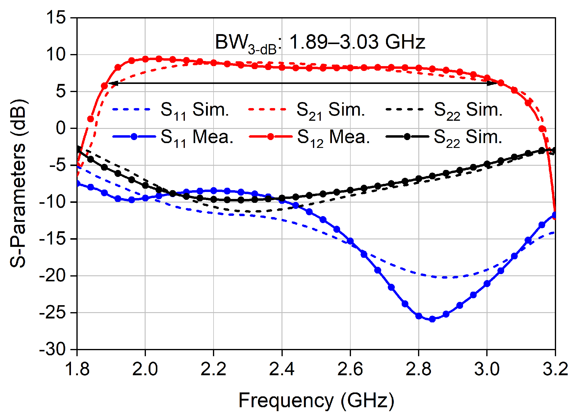
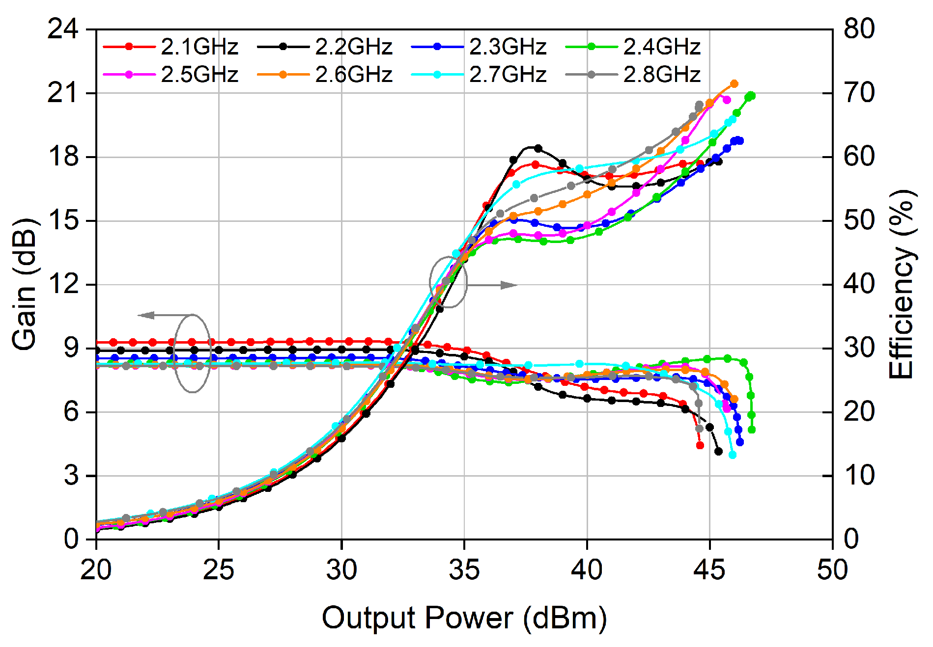
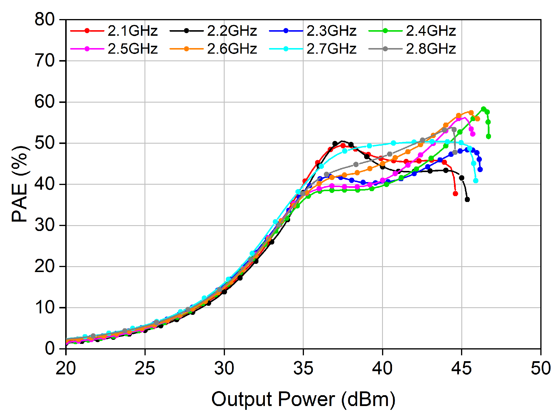
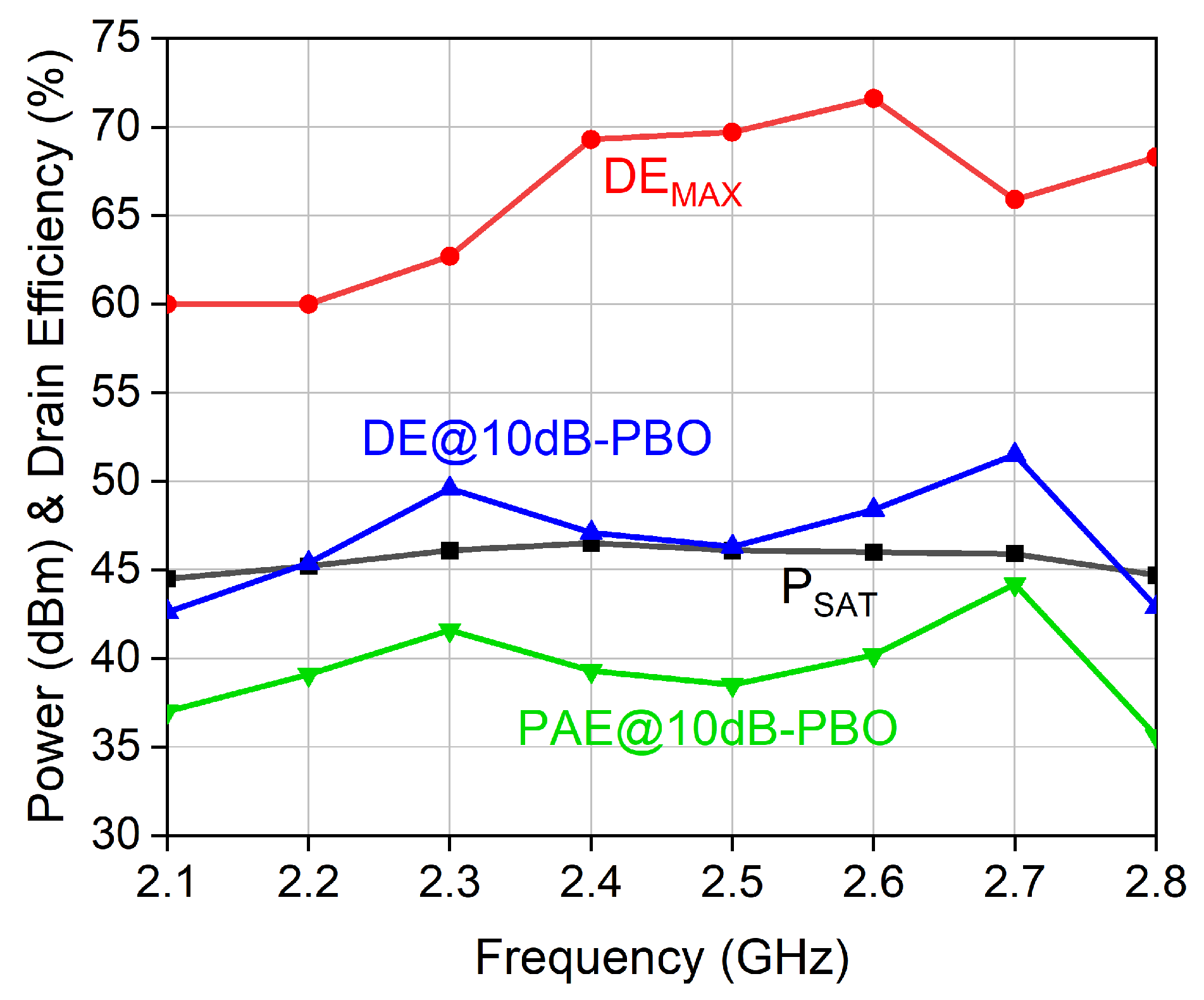
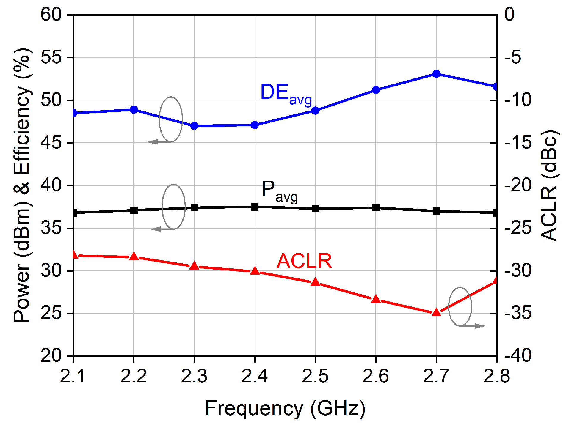
4. Measurement Results

Figure 13a presents a photograph of the fabricated DPA, which occupies an area of 66 mm × 65 mm . The DPA was mounted on a heat sink to dissipate heat during operation. Continuous-wave (CW) and modulated signal measurements were conducted. The supply voltages for the Main and Auxiliary PAs were set to 28 V and 32 V, respectively. The gate bias voltage for the Main PA was set to −2.7 V to obtain a quiescent current of 200 mA. The gate bias voltage for the Auxiliary PAs was −5.4 V.
As illustrated in Figure 13b, a signal generator was used to generate the requisite input signal, and a broadband linear driver was positioned between the signal generator and the fabricated DPA to amplify the input power. A spectrum analyzer was utilized to monitor the output signal, with a 30 dB attenuator inserted preceding it. Several DC voltage suppliers were employed to provide the DC voltages.
The measured small-signal S-parameters of the fabricated DPA are depicted in Figure 14, which includes a comparison between the measured and simulated results. The PA achieves a wide 3 dB gain bandwidth ( B W 3 d B ) of 1.14 GHz, spanning from 1.89 to 3.03 GHz, with a peak gain of 9.4 dB at 2.05 GHz. Across the frequencies within the 3 dB bandwidth, the input is well matched with S 11 below −8.5 dB.
The large-signal CW results measured in the frequency range of 2.1–2.8 GHz are shown in Figure 15, and the measured power-added efficiency (PAE) is presented in Figure 16. The large-signal performance versus frequency is summarized in Figure 17. Within the frequencies of 2.1–2.8 GHz, the PA exhibits a high P s a t , ranging from 44.5 to 46.5 dBm. The DE at saturation is in the range of 60–72%. In the deep OBO region of up to 10 dB, the PA still maintains a high measured DE from 43% to 52%, and the corresponding PAE is in the range of 36–44%. The measured results show good agreement with the simulated results, thereby validating the proposed concept.
The linearity of the PA is evaluated using a 20 MHz long-term evolution (LTE) signal with 8.5 dB PAPR. The measured output signal spectra without any digital predistortion (DPD) at several representative frequencies are presented in Figure 18. The measured modulation results over the whole operating frequency band are illustrated in Figure 19. The PA achieves a high average drain efficiency ( DE avg ) of 47–53% at an average output power ( P avg ) of 36.8–37.5 dBm. Notably, the PA exhibits a low adjacent channel leakage ratio (ACLR) ranging from −35 to −28.2 dBc without any DPD, which is attributable to the intrinsic high linearity of the series Doherty topology [8].
The CW and modulation performance comparisons of the proposed PA with prior-art three-way parallel DPAs and LMBAs are presented in Table 1 and Table 2, respectively. Owing to the low ITR of the proposed three-way series Doherty topology, this DPA demonstrates a high P s a t of 44.5–46.5 dBm and a high efficiency of 60–72%/43–52% at saturation/10 dB OBO across a broad bandwidth of 2.1–2.8 GHz, corresponding to a fractional bandwidth (FBW) of 28.6%. Notably, as can be seen from Table 2, this DPA exhibits a better linearity with a lower ACLR of −35–−28.2 dBc without any DPD. This can be attributed to the elimination of the λ /4 TL after the Main PA in the series Doherty topology [8]. Conversely, three-way LMBAs are prone to significant nonlinear gain compression during load modulation, resulting in a compromised linearity [24,25,26]. In summary, the proposed DPA exhibits outstanding performance in terms of bandwidth, efficiency, and linearity.

5. Conclusions

In this article, a new broadband three-way series Doherty topology is proposed. This topology enables a broadband output power back-off (OBO) efficiency enhancement of up to 10 dB or higher by arranging the power ratio of the Main PA and the Auxiliary PAs. A transformer is employed for Doherty load modulation and three-way power combining, and it requires only a low coupling factor. This characteristic facilitates the implementation of the proposed topology in double-sided PCBs or MMIC processes. The theory and design methodology of the proposed topology are discussed in detail. Experimental validation through the fabrication of a prototype DPA demonstrates its capability to achieve a high efficiency, wide bandwidth, and deep OBO range for both CW and modulated signal measurements. In addition, it is noteworthy that the PA achieves an ACLR of as low as −35 to −28.2 dBc without DPD, which can be attributed to the intrinsic high linearity of the series Doherty topology.

Author Contributions

Conceptualization, X.Q. and Y.W.; methodology, X.Q.; software, X.Q.; validation, X.Q., J.L. and Y.W.; formal analysis, X.Q.; investigation, X.Q.; resources, X.Q.; data curation, X.Q.; writing—original draft preparation, X.Q.; writing—review and editing, Y.W.; visualization, X.Q.; supervision, Y.W.; project administration, Y.W.; funding acquisition, Y.W. All authors have read and agreed to the published version of the manuscript.

Funding

This work was supported by the Fundamental Research Funds for the Central Universities under Grant No. 2020ZYGXZR067.

Data Availability Statement

The data that support the findings of this study are available from the corresponding author, Yanjie Wang, upon reasonable request.

Conflicts of Interest

The authors declare no conflicts of interest.

References

  1. Yang, B.; Yu, Z.; Lan, J.; Zhang, R.; Zhou, J.; Hong, W. Digital beamforming-based massive MIMO transceiver for 5G millimeter-wave communications. IEEE Trans. Microw. Theory Techn. 2018, 66, 3403–3418. [Google Scholar] [CrossRef]
  2. Zaidi, A.; Baldemair, R.; Molés-Cases, V.; He, N.; Werner, K.; Cedergren, A. OFDM numerology design for 5G new radio to support IoT, eMBB, and MBSFN. IEEE Commun. Stand. Mag. 2018, 2, 78–83. [Google Scholar] [CrossRef]
  3. Wang, F.; Wang, H. A broadband linear ultra-compact mm-wave power amplifier with distributed-balun output network: Analysis and design. IEEE J. Solid-State Circuits 2021, 56, 2308–2323. [Google Scholar] [CrossRef]
  4. Garay, E.F.; Munzer, D.J.; Wang, H. A mm-wave power amplifier for 5G communication using a dual-drive topology exhibiting a maximum PAE of 50% and maximum DE of 60% at 30GHz. In Proceedings of the 2021 IEEE International Solid-State Circuits Conference, San Francisco, CA, USA, 13–22 February 2021; pp. 258–260. [Google Scholar]
  5. Park, H.-C.; Kim, S.; Lee, J.; Jung, J.; Baek, S.; Kim, T.; Kang, D.; Minn, D.; Yang, S.-G. Single transformer-based compact Doherty power amplifiers for 5G RF phased-array ICs. IEEE J. Solid-State Circuits 2022, 57, 1267–1279. [Google Scholar] [CrossRef]
  6. de Almeida, J.V.; Gu, X.; Hussain, I.; Wu, K. High-efficiency moderate-power amplifier using packaged GaN transistor with improved average PAE and gain for batteryless IoT applications. IEEE Trans. Microw. Theory Techn. 2023, 71, 628–639. [Google Scholar] [CrossRef]
  7. Cho, Y.; Kang, D.; Kim, J.; Moon, K.; Park, B.; Kim, B. Linear Doherty power amplifier with an enhanced back-off efficiency mode for handset applications. IEEE Trans. Microw. Theory Techn. 2014, 62, 567–578. [Google Scholar] [CrossRef]
  8. Pashaeifar, M.; de Vreede, L.C.; Alavi, M.S. A millimeter-wave CMOS series-Doherty power amplifier with post-silicon inter-stage passive validation. IEEE J. Solid-State Circuits 2022, 57, 2999–3013. [Google Scholar] [CrossRef]
  9. Zong, Z.; Tang, X.; Khalaf, K.; Yan, D.; Mangraviti, G.; Nguyen, J.; Liu, Y.; Wambacq, P. A 28-GHz SOI-CMOS Doherty power amplifier with a compact transformer-based output combiner. IEEE Trans. Microw. Theory Techn. 2021, 69, 2795–2808. [Google Scholar] [CrossRef]
  10. Cho, Y.; Moon, K.; Park, B.; Kim, J.; Kim, B. Voltage-combined CMOS Doherty power amplifier based on transformer. IEEE Trans. Circuits Syst. II Exp. Briefs 2016, 64, 3612–3622. [Google Scholar] [CrossRef]
  11. Zhao, C.; Liu, H.; Wu, Y.; Kang, K. Analysis and design of CMOS Doherty power amplifier based on voltage combining method. IEEE Access 2017, 5, 5001–5012. [Google Scholar] [CrossRef]
  12. Mortazavi, M.; Shen, Y.; Mul, D.; de Vreede, L.C.N.; Spirito, M.; Babaie, M. A four-way series Doherty digital polar transmitter at mm-wave frequencies. IEEE J. Solid-State Circuits 2022, 57, 803–817. [Google Scholar] [CrossRef]
  13. Wang, F.; Wang, H. A high-power broadband multi-primary DAT-based Doherty power amplifier for mm-wave 5G applications. IEEE J. Solid-State Circuits 2021, 56, 1668–1681. [Google Scholar] [CrossRef]
  14. Li, J.; Yin, Y.; Chen, H.; Lin, J.; Li, Y.; Jia, X.; Hu, Z.; Liu, Z.; Zhang, X.; Xu, H. A transformer-based quadrature Doherty digital power amplifier with 4.1 W peak power in 28 nm bulk CMOS. J. Solid-State Circuits 2023, 58, 3296–3307. [Google Scholar] [CrossRef]
  15. Shi, W.; Shi, W.; Peng, J.; Feng, L.; Gao, Y.; He, S.; Yue, C.P. Design and analysis of continuous-mode Doherty power amplifier with second harmonic control. IEEE Trans. Circuits Syst. II Exp. Briefs 2021, 68, 2247–2251. [Google Scholar] [CrossRef]
  16. Liu, R.-J.; Zhu, X.-W.; Xia, J.; Zhao, Z.-M.; Dong, Q.; Chen, P.; Zhang, L.; Jiang, X.; Yu, C.; Hong, W. A 24-28-GHz GaN MMIC synchronous Doherty power amplifier with enhanced load modulation for 5G mm-wave applications. IEEE Trans. Microw. Theory Techn. 2022, 70, 3910–3922. [Google Scholar] [CrossRef]
  17. Nasri, A.; Estebsari, M.; Toofan, S.; Piacibello, A.; Pirola, M.; Camarchia, V.; Ramella, C. Design of a wideband Doherty power amplifier with high efficiency for 5G application. Electronics 2021, 10, 873. [Google Scholar] [CrossRef]
  18. Donati Guerrieri, S.; Catoggio, E.; Bonani, F. Analysis of Doherty power amplifier matching assisted by physics-based device modelling. Electronics 2023, 12, 2101. [Google Scholar] [CrossRef]
  19. Liang, C.; Roblin, P.; Hahn, Y.; Martinez-Lopez, J.I.; Chang, H.-C.; Chen, V. Single-input broadband hybrid Doherty power amplifiers design relying on a phase sliding-mode of the load modulation scheme. IEEE Trans. Microw. Theory Techn. 2023, 71, 1550–1562. [Google Scholar] [CrossRef]
  20. Grebennikov, A. A high-efficiency 100-W four-stage Doherty GaN HEMT power amplifier module for WCDMA systems. In Proceedings of the 2011 IEEE MTT-S International Microwave Symposium, Baltimore, MD, USA, 5–10 June 2011; pp. 1–10. [Google Scholar]
  21. Chen, S.; Wang, W.; Xu, K.; Wang, G. A reactance compensated three-device Doherty power amplifier for bandwidth and back-off range extension. Wirel. Commun. Mobile Comput. 2018, 2018, 8418165. [Google Scholar] [CrossRef]
  22. Zhou, H.; Perez-Cisneros, J.-R.; Hesami, S.; Buisman, K.; Fager, C. A generic theory for design of efficient three-stage Doherty power amplifiers. IEEE Trans. Microw. Theory Techn. 2022, 70, 1242–1253. [Google Scholar] [CrossRef]
  23. Dietrich, F.; Wei, M.-D.; Heidebrecht, E.; Bierbüsse, D.; Negra, R. Load and frequency independent Doherty power amplifier back-off extension. IEEE Trans. Microw. Theory Techn. 2024; in press. [Google Scholar] [CrossRef]
  24. Pang, J.; Li, Y.; Li, M.; Zhang, Y.; Zhou, X.Y.; Dai, Z.; Zhu, A. Analysis and design of highly efficient wideband RF-input sequential load modulated balanced power amplifier. IEEE Trans. Microw. Theory Techn. 2020, 68, 1741–1753. [Google Scholar] [CrossRef]
  25. Sun, J.; Lin, F.; Sun, H.; Chen, W.; Negra, R. Broadband three-stage pseudoload modulated balanced amplifier with power back-off efficiency enhancement. IEEE Trans. Microw. Theory Techn. 2022, 70, 2710–2722. [Google Scholar] [CrossRef]
  26. Quaglia, R.; Cripps, S. A load modulated balanced amplifier for telecom applications. IEEE Trans. Microw. Theory Techn. 2018, 66, 1328–1338. [Google Scholar] [CrossRef]
  27. Cao, Y.; Chen, K. Pseudo-Doherty load-modulated balanced amplifier with wide bandwidth and extended power back-off range. IEEE Trans. Microw. Theory Techn. 2020, 68, 3172–3183. [Google Scholar] [CrossRef]
  28. Cao, Y.; Chen, K. Hybrid asymmetrical load modulated balanced amplifier with wide bandwidth and three-way-Doherty efficiency enhancement. IEEE Trans. Microw. Theory Techn. 2021, 31, 721–724. [Google Scholar] [CrossRef]
  29. Chu, C.; Sharma, T.; Dhar, S.K.; Darraji, R.; Wang, X.; Pang, J.; Zhu, A. Waveform engineered sequential load modulated balanced amplifier with continuous Class-F-1 and Class-J operation. IEEE Trans. Microw. Theory Techn. 2022, 70, 1269–1283. [Google Scholar] [CrossRef]
  30. Que, X.; Wang, Y.; Huang, S. A 6-/12-dB back-off reconfigurable Doherty-like load modulated balanced amplifier with compact area and wide bandwidth. Microelectron. J. 2024, 148, 106198. [Google Scholar] [CrossRef]
  31. Maktoomi, M.H.; Ren, H.; Marbell, M.N.; Klein, V.; Wilson, R.; Arigong, B. A wideband isolated real-to-complex impedance transforming uniplanar microstrip line balun for push–pull power amplifier. IEEE Trans. Microw. Theory Techn. 2020, 68, 4560–4569. [Google Scholar] [CrossRef]
  32. Smolarz, R.; Gruszczynski, S.; Wincza, K. Multisection ultra-broadband directional coupler designed in MMIC technology. IEEE Access 2021, 9, 33478–33486. [Google Scholar] [CrossRef]
  33. Standard IPC-2221A; Generic Standard on Printed Board Design—A Standard Developed by IPC. IPC: Northbrook, IL, USA, 2003.
  34. El-Gharniti, O.; Kerherve, E.; Begueret, J.-B. Modeling and characterization of on-chip transformers for silicon RFIC. IEEE Trans. Microw. Theory Techn. 2007, 55, 607–615. [Google Scholar] [CrossRef]
Figure 1. (a) Parallel Doherty topology. (b) Series Doherty topology.
Electronics 13 01882 g001
Figure 2. (a) Proposed three-way Doherty topology. (b) Realization of the transformer using coupled inductors. (c) Shortening of the λ / 4 TL. (d) Integrating C 02 with C p .
Electronics 13 01882 g002
Figure 3. Normalized impedance ( R L / Z 3 , s a t ) and OBO range under various α values.
Electronics 13 01882 g003
Figure 4. Efficiency versus OBO under various α values.
Electronics 13 01882 g004
Figure 5. Load modulations of the Main PA and Auxiliary PAs under α = 1 .
Electronics 13 01882 g005
Figure 6. Optimal load impedance with maximum output power obtained from load-pull simulation.
Electronics 13 01882 g006
Figure 7. (a) Layout of the output network. (b) EM simulation and other parameters of the output network.
Electronics 13 01882 g007
Figure 8. (a) Practical coupled coils model containing parasitic capacitors C m , C g p , and C g s . (b) Values of the parasitic capacitors and resonant inductors in the proposed output network.
Electronics 13 01882 g008
Figure 9. (a) Load impedances of the Auxiliary PAs at saturation. (b) Load impedances of the Main PA at saturation and 9.5 dB OBO.
Electronics 13 01882 g009
Figure 10. Schematic of the designed DPA. Transmission line width and length (W/L) are given in millimeters.
Electronics 13 01882 g010
Figure 11. Simulated drain efficiency and gain versus output power within the frequency range of 2.1–2.8 GHz.
Electronics 13 01882 g011
Figure 12. Simulated load impedance at the drain of the Main PA and output currents of the Main, Aux.1, and Aux.2 PAs versus output power at 2.5 GHz.
Electronics 13 01882 g012
Figure 13. (a) Photograph of the fabricated PA. (b) Measurement setup.
Electronics 13 01882 g013
Figure 14. Measured and simulated S-parameters of the proposed PA.
Electronics 13 01882 g014
Figure 15. Measured drain efficiency and gain versus output power within the frequency range of 2.1–2.8 GHz.
Electronics 13 01882 g015
Figure 16. Measured PAE versus output power within the frequency range of 2.1–2.8 GHz.
Electronics 13 01882 g016
Figure 17. Measured CW results of the proposed PA.
Electronics 13 01882 g017
Figure 18. Output spectra of 20 MHz LTE signal with 8.5 dB PAPR at (a) 2.4 GHz and (b) 2.7 GHz without DPD.
Electronics 13 01882 g018
Figure 19. Measured modulation results of the proposed PA.
Electronics 13 01882 g019
Table 1. CW performance comparison of the proposed PA with prior-art three-way load modulation PAs.
Ref.ArchitectureFreq. (GHz)FBW (%)Gain (dB) P sat (dBm) DE@P sat (%)OBO (dB)DE@OBO (%)
This workthree-way series DPA2.1–2.828.68.2–9.344.5–46.560–721043–52
[21]three-way parallel DPA2.0–2.6268–1243.6–45.453–76841–48
[22]three-way parallel DPA2.04–2.249.3843.7–45.350–681029–56
[23]reflective-type DPA2.1–3.0357.5–1146.6–4948–5819/933–50
[24]SLMBA a3.05–3.5515.29.5–10.342.3–43.761–751043–51
[25]pseudo-LMBA1.6–2.022.28.5–9.743.4–4465–751049–62
a SLMBA: sequential load-modulated balanced power amplifier.
Table 2. Modulation performance comparison of the proposed PA with prior-art three-way load modulation PAs.
Ref.Freq. (GHz)ModulationPAPR (dB) P avg (dBm) DE avg (%) ACLR  b (dBc)
This work2.1–2.820 MHz LTE8.536.8–37.547–53−35–−28.2
[21]2.320 MHz LTE836.646−29
[22]2.1420 MHz LTE8.536.856.6−28.6
[23]2.1–3.020 MHz LTE94045–52−27–−23
[24]3.05–3.5540 MHz LTE835.557.8−26
[25]1.6–2.020 MHz LTE10.3233.6–34.542.8–54.6−30.76–−23.5
b without DPD.
Disclaimer/Publisher’s Note: The statements, opinions and data contained in all publications are solely those of the individual author(s) and contributor(s) and not of MDPI and/or the editor(s). MDPI and/or the editor(s) disclaim responsibility for any injury to people or property resulting from any ideas, methods, instructions or products referred to in the content.

