


How to Accurately Determine the Ohmic Contact Properties on n-Type 4H-SiC


Abstract
1. Introduction
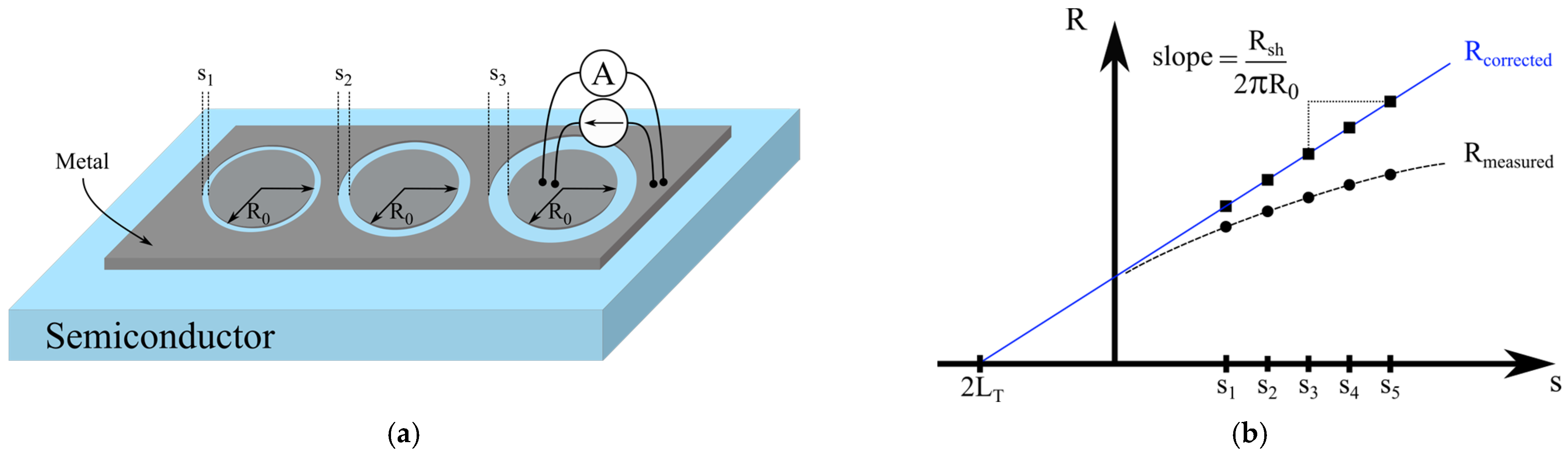
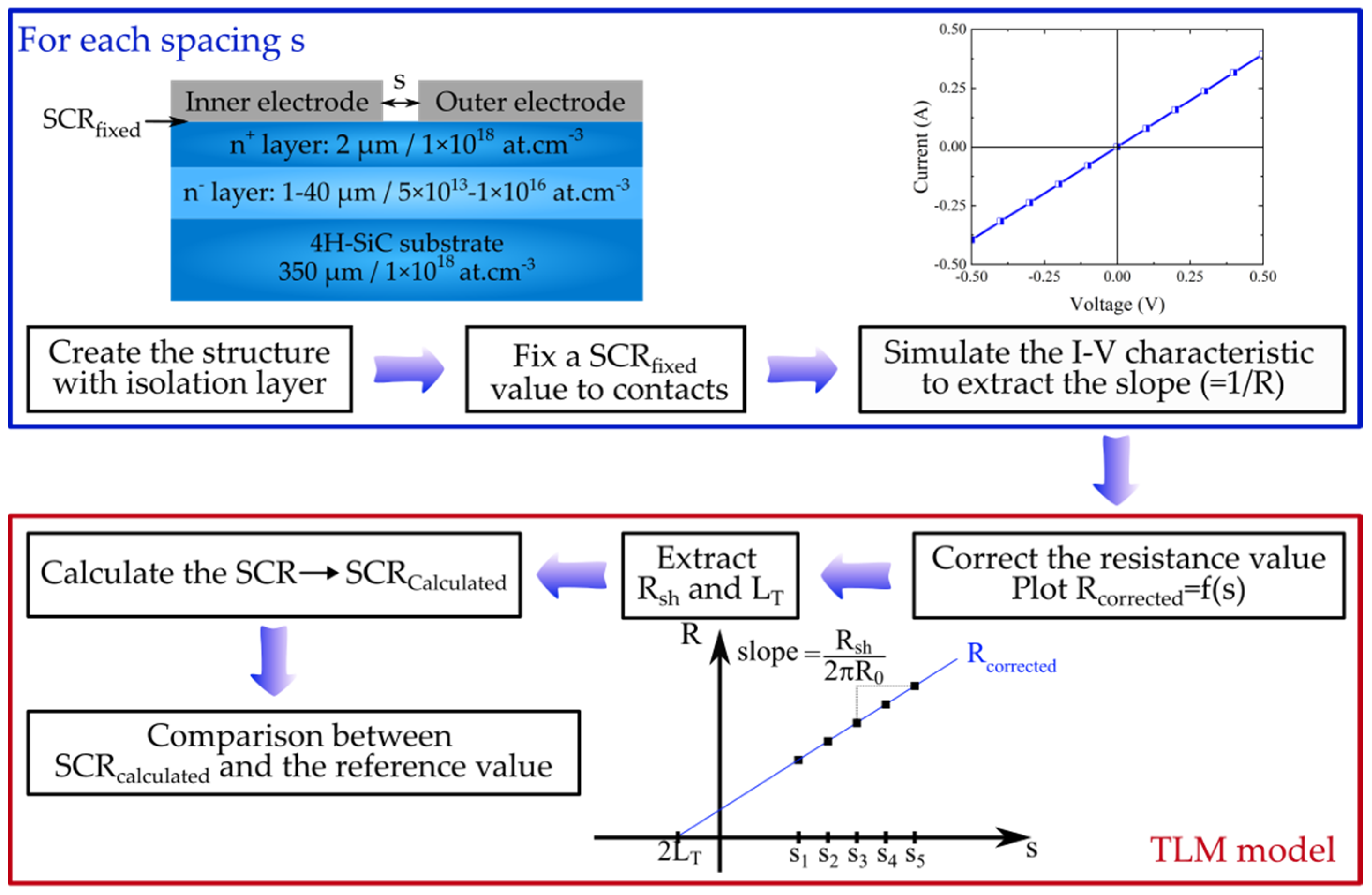
2. TLM Model
3. Motivations
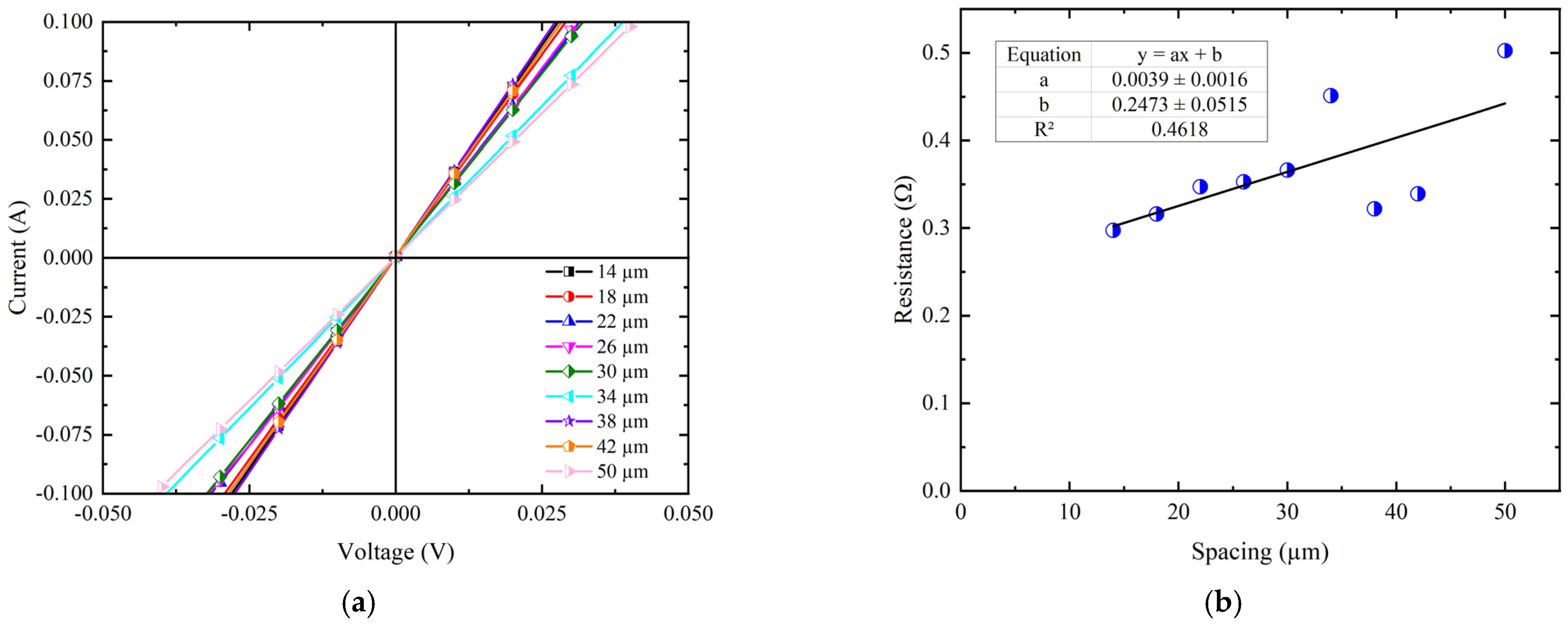
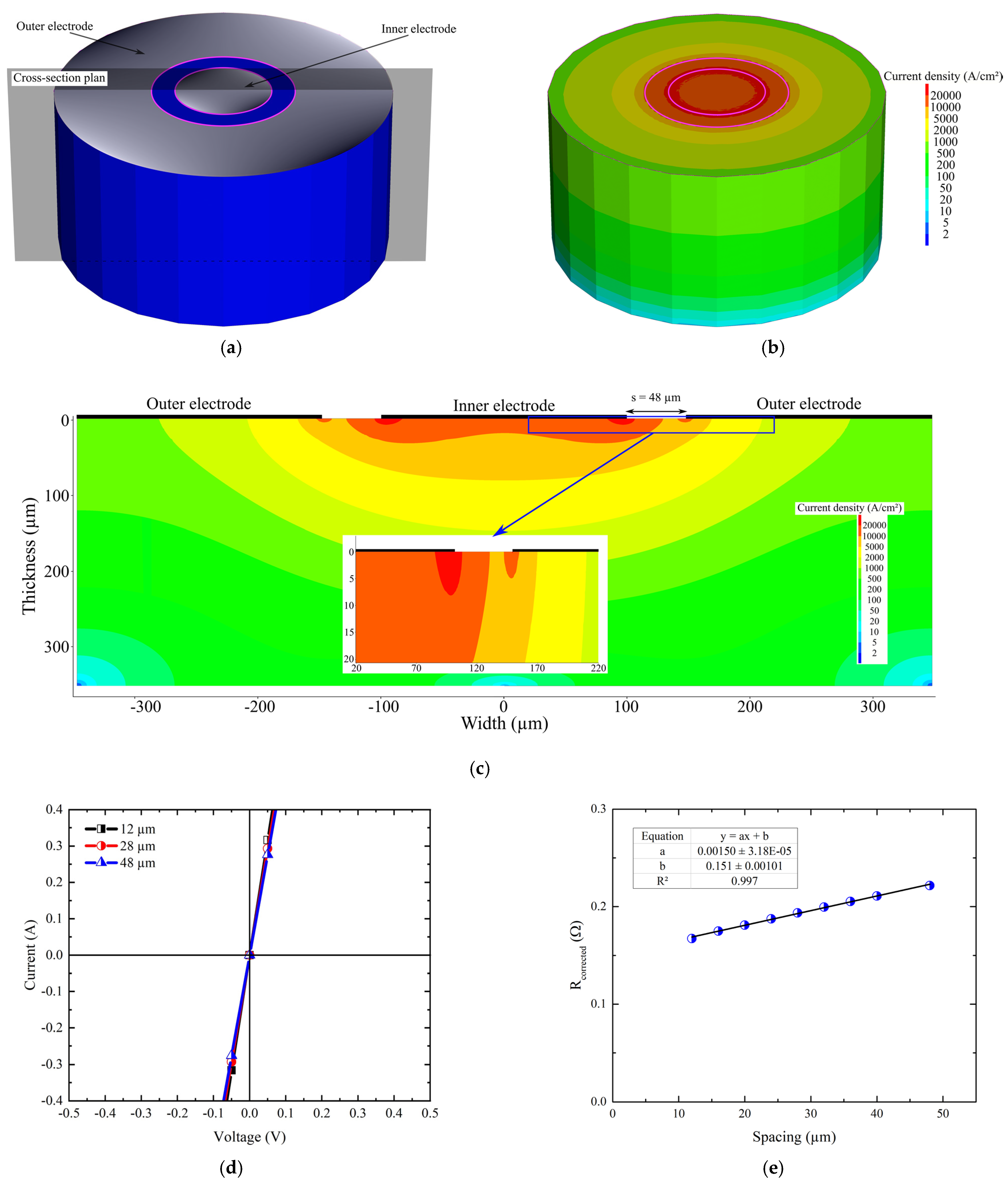
3.1. Simulations of c-TLM Structures onto 350 µm-Thick 4H-SiC Substrate
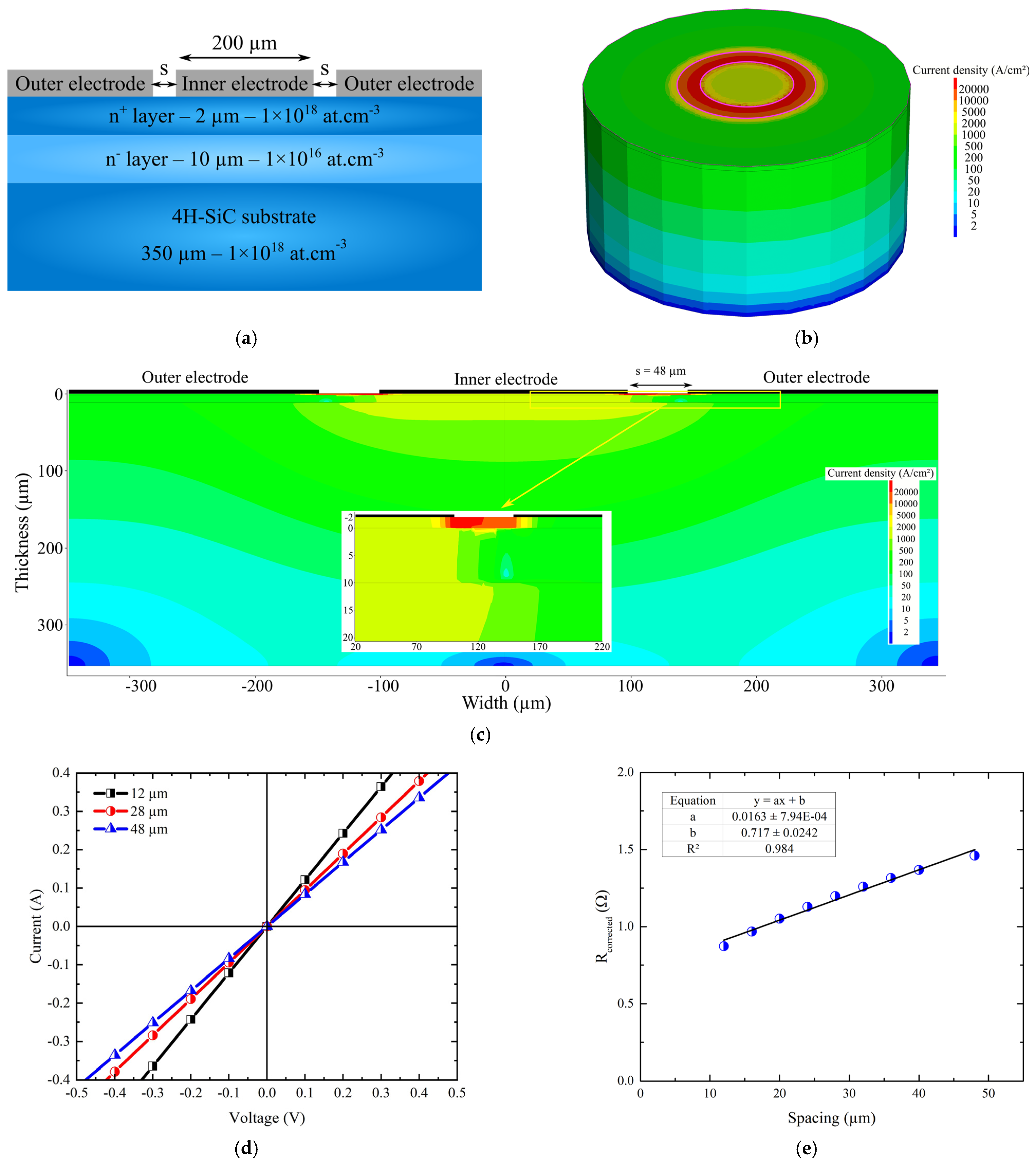
3.2. Simulations of c-TLM Structures onto 2 µm Thick 4H-SiC Substrate
3.3. Simulations of c-TLM Structures with an Electrical Isolation of the 4H-SiC Substrate
4. Design and Methods
5. Simulation Results
5.1. Influence of the Layer Thickness Undermeath the Electrodes on the SCR Determination
5.2. Influence of the Isolation Layer on the SCR Determination
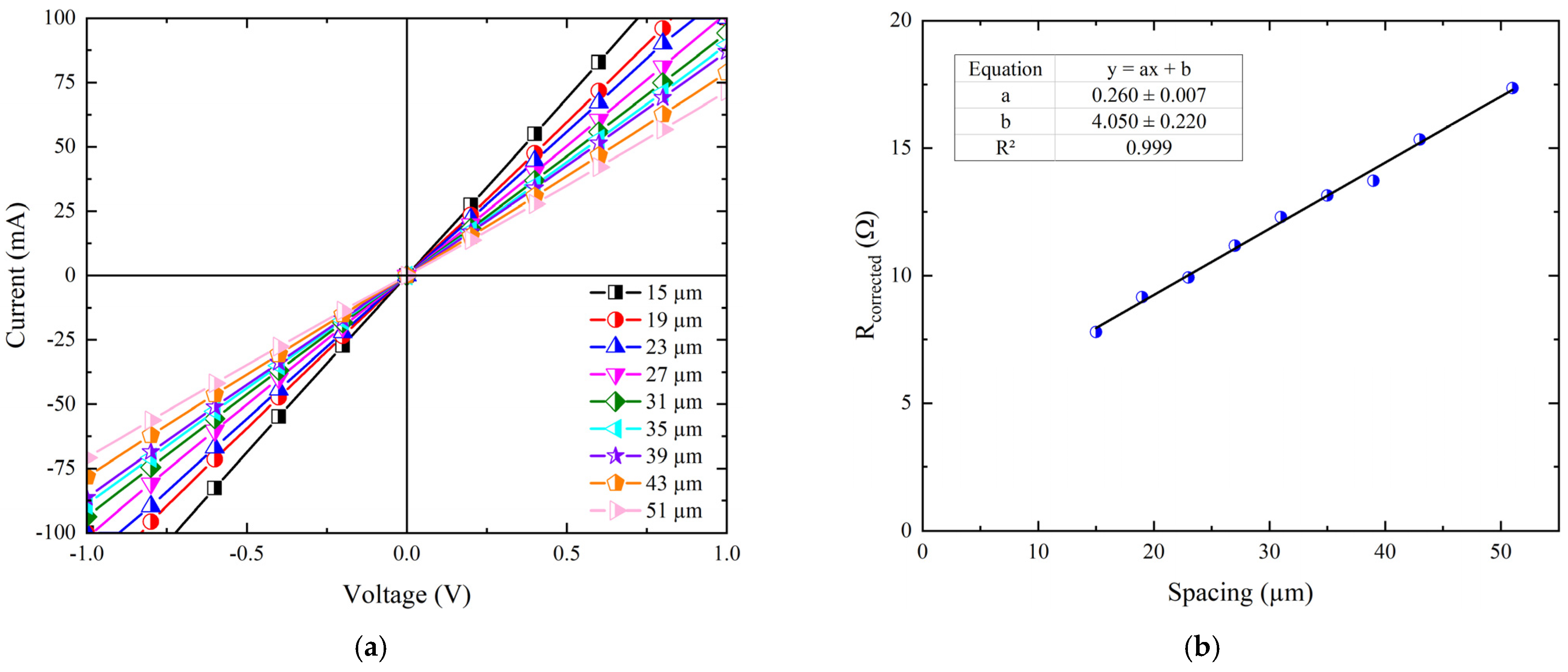
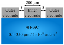
6. Experimental Results with 5 µm Thick Isolation Layer Doped at 5 × 10¹³ at·cm−3
7. Conclusions
Author Contributions
Funding
Data Availability Statement
Conflicts of Interest
References
- Crofton, J.; Porter, L.M.; Williams, J.R. The Physics of Ohmic Contacts to SiC. Phys. Status Solidi B 1997, 202, 581–603. [Google Scholar] [CrossRef]
- Chang, S.-C.; Wang, S.-J.; Uang, K.-M.; Liou, B.-W. Investigation of Au/Ti/Al Ohmic Contact to N-Type 4H–SiC. Solid State Electron. 2005, 49, 1937–1941. [Google Scholar] [CrossRef]
- Ghandi, R.; Lee, H.S.; Domeij, M.; Zetterling, C.M.; Östling, M. Backside Nickel Based Ohmic Contacts to N-Type Silicon Carbide. Mater. Sci. Forum 2008, 600–603, 635–638. [Google Scholar] [CrossRef]
- Han, L.; Shen, H.; Liu, K.; Wang, Y.; Tang, Y.; Bai, Y.; Xu, H.; Wu, Y.; Liu, X. Improved Adhesion and Interface Ohmic Contact on N-Type 4H-SiC Substrate by Using Ni/Ti/Ni. J. Semicond. 2014, 35, 072003. [Google Scholar] [CrossRef]
- Ito, K.; Onishi, T.; Takeda, H.; Kohama, K.; Tsukimoto, S.; Konno, M.; Suzuki, Y.; Murakami, M. Simultaneous Formation of Ni/Al Ohmic Contacts to Both n- and p-Type 4H-SiC. J. Electron. Mater. 2008, 37, 1674–1680. [Google Scholar] [CrossRef]
- Cho, N.-I.; Jung, K.-H.; Choi, Y. Improved Ohmic Contact to the N-Type 4H-SiC Semiconductor Using Cobalt Silicides. Semicond. Sci. Technol. 2004, 19, 306–310. [Google Scholar] [CrossRef]
- Rupp, R.; Kern, R.; Gerlach, R. Laser Backside Contact Annealing of SiC Power Devices: A Prerequisite for SiC Thin Wafer Technology. In Proceedings of the 2013 25th International Symposium on Power Semiconductor Devices & IC’s (ISPSD), Kanazawa, Japan, 26–30 May 2013; pp. 51–54. [Google Scholar]
- Berger, C.; Michaud, J.F.; Chouteau, D.; Alquier, D. Laser Annealing Simulations of Metallisations Deposited on 4H-SiC. Mater. Sci. Forum 2019, 963, 502–505. [Google Scholar] [CrossRef]
- Ding, J.; Li, X.; Yang, K.; Zhu, Y. Numerical Simulation on Controlling the Front-Side Temperature of Thinned SiC Substrate during Ohmic Contact to Ni or Ti Using Back-Side Laser Annealing. J. Appl. Phys. 2022, 132, 035703. [Google Scholar] [CrossRef]
- De Silva, M.; Kawasaki, T.; Miyazaki, T.; Koganezawa, T.; Yasuno, S.; Kuroki, S.-I. Formation of Epitaxial Ti-Si-C Ohmic Contact on 4H-SiC C Face Using Pulsed-Laser Annealing. Appl. Phys. Lett. 2017, 110, 252108. [Google Scholar] [CrossRef]
- Berger, C.; Alquier, D.; Bah, M.; Michaud, J.-F. Electrical, Morphological and Structural Properties of Ti Ohmic Contacts Formed on n-Type 4H–SiC by Laser Thermal Annealing. Mater. Sci. Semicond. 2022, 151, 106983. [Google Scholar] [CrossRef]
- Rascunà, S.; Badalà, P.; Tringali, C.; Bongiorno, C.; Smecca, E.; Alberti, A.; Di Franco, S.; Giannazzo, F.; Greco, G.; Roccaforte, F.; et al. Morphological and Electrical Properties of Nickel Based Ohmic Contacts Formed by Laser Annealing Process on N-Type 4H-SiC. Mater. Sci. Semicond. 2019, 97, 62–66. [Google Scholar] [CrossRef]
- Badalà, P.; Deretzis, I.; Sanzaro, S.; Pennisi, F.M.; Bongiorno, C.; Fisicaro, G.; Rascunà, S.; Bellocchi, G.; Bassi, A.; Boscaglia, M.; et al. Ni-Silicide Ohmic Contacts on 4H-SiC Formed by Multi Pulse Excimer Laser Annealing. Solid State Phenom. 2023, 344, 15–22. [Google Scholar] [CrossRef]
- Zhou, Z.; He, W.; Zhang, Z.; Sun, J.; Schöner, A.; Zheng, Z. Characteristics of Ni-Based Ohmic Contacts on n-Type 4H-SiC Using Different Annealing Methods. Nanotechnol. Precis. Eng. 2021, 4, 013006. [Google Scholar] [CrossRef]
- Cheng, Y.; Lu, W.; Wang, T.; Chen, Z. Fabrication of Ohmic Contact on Semi-Insulating 4H-SiC Substrate by Laser Thermal Annealing. J. Appl. Phys. 2016, 119, 225705. [Google Scholar] [CrossRef]
- Schroder, D.K. Semiconductor Material and Device Characterization, 3rd ed.; John Wiley & Sons: Hoboken, NJ, USA, 2006; ISBN 978-0-471-73906-7. [Google Scholar]
- Cao, Y.; Perez-Garcıa, S.A.; Nyborg, L. Investigation of Ni/Ta Contacts on 4H Silicon Carbide upon Thermal Annealing. Appl. Surf. Sci. 2007, 254, 139–142. [Google Scholar] [CrossRef]
- Kuchuk, A.; Kladko, V.; Guziewicz, M.; Piotrowska, A.; Minikayev, R.; Stonert, A.; Ratajczak, R. Fabrication and Characterization of Nickel Silicide Ohmic Contacts to N-Type 4H Silicon Carbide. J. Phys. Conf. Ser. 2008, 100, 042003. [Google Scholar] [CrossRef]
- Jiang, S.-Y.; Li, X.-Y.; Chen, Z.-Z. Role of W in W/Ni Bilayer Ohmic Contact to n-Type 4H-SiC from the Perspective of Device Applications. IEEE Trans. Electron. Devices 2018, 65, 641–647. [Google Scholar] [CrossRef]
- Wang, Z.; Liu, W.; Wang, C. Recent Progress in Ohmic Contacts to Silicon Carbide for High-Temperature Applications. J. Electron. Mater. 2016, 45, 267–284. [Google Scholar] [CrossRef]
- Roccaforte, F.; La Via, F.; Raineri, V. Ohmic contacts to SiC. Int. J. High Speed Electron. Syst. 2005, 15, 781–820. [Google Scholar] [CrossRef]
- Rideout, V.L. A Review of the Theory, Technology and Applications of Metal-Semiconductor Rectifiers. Thin Solid Film. 1978, 48, 261–291. [Google Scholar] [CrossRef]
- Kawahara, K.; Suda, J.; Pensl, G.; Kimoto, T. Reduction of Deep Levels Generated by Ion Implantation into N- and p-Type 4H–SiC. J. Appl. Phys. 2010, 108, 033706. [Google Scholar] [CrossRef]
- Michaud, J.F.; Song, X.; Biscarrat, J.; Cayrel, F.; Collard, E.; Alquier, D. Aluminum Implantation in 4H-SiC: Physical and Electrical Properties. Mater. Sci. Forum 2012, 740–742, 581–584. [Google Scholar] [CrossRef]
- Han, S.Y.; Kim, K.H.; Kim, J.K.; Jang, H.W.; Lee, K.H.; Kim, N.-K.; Kim, E.D.; Lee, J.-L. Ohmic Contact Formation Mechanism of Ni on n-Type 4H–SiC. Appl. Phys. Lett. 2001, 79, 1816–1818. [Google Scholar] [CrossRef]
- Klootwijk, J.H.; Timmering, C.E. Merits and Limitations of Circular TLM Structures for Contact Resistance Determination for Novel 111-V HBTs. In Proceedings of the 2004 International Conference on Microelectronic Test Structures (IEEE Cat. No. 04CH37516), Awaji, Japan, 22–25 March 2004. [Google Scholar]
- Michaud, J.F.; Berger, C.; Alquier, D. Nickel Ohmic Contacts Formed on 4H-SiC by UV Laser Annealing. In Proceedings of the International Conference on Silicon Carbide and Related Materials (ICSCRM), Sorrento, Italy, 17–22 September 2023. [Google Scholar]


| SCRfixed | |||||||||
|---|---|---|---|---|---|---|---|---|---|
| 10−3 Ω·cm2 | 10−4 Ω·cm2 | 10−5 Ω·cm2 | 10−6 Ω·cm2 | ||||||
 | 4H-SiC thickness (µm) | SCRcalculated (×10−3 Ω·cm2) | SCRcalculated (×10−4 Ω·cm2) | SCRcalculated (×10−5 Ω·cm2) | SCRcalculated (×10−6 Ω·cm2) | ||||
| 350 | 1.41 | ⚠ | 1.49 | ⚠ | 2.38 | ⚠ | 9.99 | ⚠ | |
| 10 | 1.20 | ⚠ | 1.01 | ⚠ | 1.16 | 2.62 | |||
| 5 | 1.12 | ⚠ | 0.98 | 1.06 | 1.84 | ||||
| 2 | 1.03 | ⚠ | 0.97 | 1.00 | 1.31 | ||||
| 1 | 0.99 | ⚠ | 0.96 | 0.97 | 1.14 | ||||
| 0.5 | 0.97 | 0.96 | 0.96 | 1.04 | |||||
| 0.1 | 0.96 | 0.95 | 0.93 | 0.96 | |||||
| SCRfixed | |||||||||
|---|---|---|---|---|---|---|---|---|---|
| 10−3 Ω·cm2 | 10−4 Ω·cm2 | 10−5 Ω·cm2 | 10−6 Ω·cm2 | ||||||
| Doping and thickness of the isolation | SCRcalculated (×10−3 Ω·cm2) | SCRcalculated (×10−4 Ω·cm2) | SCRcalculated (×10−5 Ω·cm2) | SCRcalculated (×10−6 Ω·cm2) | |||||
| (at·cm−3) | (µm) | ||||||||
| 1 × 10¹⁶ | 1 | 1.45 | ⚠ | 1.91 | ⚠ | 5.21 | ⚠ | 29.81 | ⚠ |
| 2 | 1.51 | ⚠ | 2.28 | ⚠ | 6.66 | ⚠ | 34.85 | ⚠ | |
| 5 | 1.56 | ⚠ | 2.33 | ⚠ | 5.37 | ⚠ | 22.13 | ||
| 10 | 1.57 | ⚠ | 2.10 | ⚠ | 3.93 | 13.28 | |||
| 20 | 1.49 | ⚠ | 1.74 | ⚠ | 2.67 | 7.25 | |||
| 40 | 1.35 | ⚠ | 1.41 | ⚠ | 1.87 | 4.13 | |||
| 5 × 10¹⁵ | 1 | 1.49 | ⚠ | 2.16 | ⚠ | 6.22 | ⚠ | 33.67 | ⚠ |
| 2 | 1.58 | ⚠ | 2.60 | ⚠ | 6.78 | ⚠ | 30.71 | ⚠ | |
| 5 | 1.57 | ⚠ | 2.13 | ⚠ | 4.01 | 13.60 | |||
| 10 | 1.50 | ⚠ | 1.76 | ⚠ | 2.71 | 7.33 | |||
| 20 | 1.37 | ⚠ | 1.44 | ⚠ | 1.90 | 4.12 | |||
| 40 | 1.23 | ⚠ | 1.22 | 1.45 | 2.65 | ||||
| 1 × 10¹⁵ | 1 | 1.64 | ⚠ | 2.62 | ⚠ | 6.14 | ⚠ | 26.02 | |
| 2 | 1.80 | ⚠ | 2.33 | ⚠ | 3.68 | 10.79 | |||
| 5 | 1.35 | ⚠ | 1.39 | 1.77 | 3.63 | ||||
| 10 | 1.21 | ⚠ | 1.19 | 1.37 | 2.32 | ||||
| 20 | 1.13 | ⚠ | 1.09 | 1.18 | 1.78 | ||||
| 40 | 1.08 | ⚠ | 1.03 | 1.10 | 1.55 | ||||
| 5 × 10¹⁴ | 1 | 1.72 | ⚠ | 2.62 | ⚠ | 5.52 | ⚠ | 21.57 | |
| 2 | 1.79 | ⚠ | 1.94 | ⚠ | 2.64 | 6.45 | |||
| 5 | 1.23 | ⚠ | 1.21 | 1.40 | 2.41 | ||||
| 10 | 1.13 | ⚠ | 1.09 | 1.18 | 1.78 | ||||
| 20 | 1.08 | ⚠ | 1.03 | 1.09 | 1.53 | ||||
| 40 | 1.06 | ⚠ | 1.01 | 1.05 | 1.42 | ||||
| 1 × 10¹⁴ | 1 | 1.80 | ⚠ | 2.50 | ⚠ | 4.74 | 16.88 | ||
| 2 | 1.55 | ⚠ | 1.44 | 1.70 | 3.19 | ||||
| 5 | 1.09 | ⚠ | 1.04 | 1.09 | 1.52 | ||||
| 10 | 1.05 | ⚠ | 1.00 | 1.04 | 1.37 | ||||
| 20 | 1.04 | ⚠ | 0.99 | 1.02 | 1.33 | ||||
| 40 | 1.04 | ⚠ | 0.99 | 1.01 | 1.32 | ||||
| 5 × 10¹³ | 1 | 1.82 | ⚠ | 2.48 | ⚠ | 4.63 | 16.23 | ||
| 2 | 1.49 | ⚠ | 1.37 | 1.58 | 2.84 | ||||
| 5 | 1.06 | ⚠ | 1.01 | 1.05 | 1.41 | ||||
| 10 | 1.04 | ⚠ | 0.99 | 1.02 | 1.32 | ||||
| 20 | 1.04 | ⚠ | 0.98 | 1.01 | 1.31 | ||||
| 40 | 1.03 | ⚠ | 0.98 | 1.01 | 1.31 | ||||
Disclaimer/Publisher’s Note: The statements, opinions and data contained in all publications are solely those of the individual author(s) and contributor(s) and not of MDPI and/or the editor(s). MDPI and/or the editor(s) disclaim responsibility for any injury to people or property resulting from any ideas, methods, instructions or products referred to in the content. |
© 2024 by the authors. Licensee MDPI, Basel, Switzerland. This article is an open access article distributed under the terms and conditions of the Creative Commons Attribution (CC BY) license (https://creativecommons.org/licenses/by/4.0/).
Share and Cite
Berger, C.; Alquier, D.; Michaud, J.-F. How to Accurately Determine the Ohmic Contact Properties on n-Type 4H-SiC. Electronics 2024, 13, 217. https://doi.org/10.3390/electronics13010217
Berger C, Alquier D, Michaud J-F. How to Accurately Determine the Ohmic Contact Properties on n-Type 4H-SiC. Electronics. 2024; 13(1):217. https://doi.org/10.3390/electronics13010217
Chicago/Turabian StyleBerger, Clément, Daniel Alquier, and Jean-François Michaud. 2024. "How to Accurately Determine the Ohmic Contact Properties on n-Type 4H-SiC" Electronics 13, no. 1: 217. https://doi.org/10.3390/electronics13010217
APA StyleBerger, C., Alquier, D., & Michaud, J.-F. (2024). How to Accurately Determine the Ohmic Contact Properties on n-Type 4H-SiC. Electronics, 13(1), 217. https://doi.org/10.3390/electronics13010217