Article

Design of a Ka-Band Heterogeneous Integrated T/R Module of Phased Array Antenna

1
Aerospace Information Research Institute, Chinese Academy of Sciences, Beijing 100101, China
2
School of Electronic Science and Engineering, University of Electronic Science and Technology of China, Chengdu 611731, China
3
Shunde Innovation School, University of Science and Technology Beijing, Foshan 528399, China
*
Author to whom correspondence should be addressed.
Electronics 2024, 13(1), 204; https://doi.org/10.3390/electronics13010204
Submission received: 18 November 2023 / Revised: 26 December 2023 / Accepted: 29 December 2023 / Published: 2 January 2024

Abstract

:
The central element of a phased array antenna that performs beam electrical scanning, as well as signal transmission and reception, is the transceiver (T/R) module. Higher standards have been set for the integration, volume, power consumption, stability, and environmental adaptability of T/R modules due to the increased operating frequency of phased array antennas, the variability of application platforms, and the diversified development of system functions. Device-based multichannel T/R modules are the key to realizing low-profile Ka-band phased array antenna microsystem architecture. The design and implementation of a low-profile, high-performance, and highly integrated Ka-band phased array antenna T/R module are examined in this paper. Additionally, a dependable Ka-band four-channel T/R module based on Si/GaAs/Low Temperature Co-fired Ceramic (LTCC), applying multi-material heterogeneous integration architecture, is proposed and fabricated. The chip architecture, transceiver link, LTCC substrates, interconnect interface, and packaging are all taken into consideration when designing the T/R module. When compared to a standard phased array antenna, the module’s profile shrunk from 40 mm to 8 mm, and its overall dimensions are only 10.8 mm × 10 mm × 3 mm. It weighs 1 g, and with the same specs, the single channel volume was reduced by 95%. The T/R module has an output power of ≥26 dBm for single-channel transmission, an efficiency of ≥25%, and a noise factor of ≤4.4 dB. When compared to T/R modules based on System-on-Chip (SOC) devices, the RF performance has significantly improved, as seen by an increase in single channel output power and a decrease in the receiving noise factor. This work lays a foundation for the devitalization and engineering application of T/R modules in highly reliable application scenarios.

1. Introduction

The phased array antenna is widely used in the field of communication [1,2,3,4,5,6]. Its flexible and agile beam scanning technology accomplishes directional communication between fast-moving and highly dynamic objects, while guaranteeing the tracking accuracy of high-speed mobile platform communication. Simultaneously, low sidelobe and bare nulls in directional diagrams can be achieved using array synthesis, enhancing the system’s ability to withstand interference and producing more dependable and stable communication lines. Because of their outstanding performance and rapid development, phased array antennas are gaining importance and are extensively applied in the field of advanced military [7,8,9,10] and commercial applications [11,12,13,14].
The central element of a phased array antenna that performs beam electrical scanning, as well as signal transmission and reception, is the T/R module. Higher standards have been set for the integration, volume, power consumption, stability, and environmental adaptability of T/R modules due to the increased operating frequency of phased array antennas, the variability of application platforms, and the diversified development of system functions [15,16,17,18].
It is essential to improve the T/R components integration to meet the development trend of phased array antennas. Due to their complicated manufacturing and assembly processes, lengthy process flows, and multiple levels of interconnection ranging from chip circuits to system integration, traditional phased array antennas have trouble meeting the cost and profile requirements of modern information systems. In contrast, millimeter-wave phased array antenna microsystems with low profile and markedly improved functional density can effectively satisfy the requirements of modern information systems for the high integration and performance of phased array antennas, making them one of the research hotspots in the industry. Among them, the devitalization of the multichannel T/R modules is the key to achieving a low-profile phased array antenna microsystem architecture.
Radar’s capacity to acquire a large instantaneous bandwidth and, consequently, improve imaging and detection accuracy can be facilitated by raising the operating frequency. The long wavelength and large bandwidth of millimeter-waves provide massive communication bandwidth attainment, enhance real-time transmission and anti-interference capabilities, and speed up communication system response [19,20,21,22]. In order to attain a broad scanning angle in a two-dimensional electric scanning array, it is imperative to reduce antenna size and enhance device integration, as the separation between array elements must be around half wavelength [23]. As demonstrated in Figure 1, millimeter-wave frequency antennas with the same aperture can attain greater SNR and EIRP values, allowing the terminal antenna to be smaller, while maintaining improved performance and energy accumulation [23].
Furthermore, the system must integrate more electronic devices with varying functions due to the devitalization and development trend of phased array antenna application scenarios. Higher requirements have been put forward to improve the integration and devitalization of T/R modules, and a low profile has become a very important factor to be considered in the design process of phased array antennas in order to avoid antenna equipment taking up too much volume on the flight platform, which affects the overall structural continuity and aerodynamic performance.

2. Related Works

Recently, both domestically and abroad, Ka-band phased array front-end microsystems were created. Table 1 lists the noteworthy accomplishments.
The comparison above makes clear how well the TR module developed in this work performs in terms of the noise coefficient, output power, and single channel volume. With a weight of 1 g and an overall dimension of only 10.8 mm × 10 mm × 3 mm, this device-based design greatly enhances T/R module integration when compared to conventional phased array antenna T/R modules. The volume of a single channel drops by 95% with the same specs. When compared to T/R modules based on SOC devices, the RF performance has significantly improved, manifested by an increase in single-channel output power and a decrease in the receiving noise factor. The single-channel output power is >26 dBm, the efficiency is ≥25%, and the noise factor is <4.4 dB thanks to the comprehensive optimization from aspects of chip architecture, transceiver link, LTCC substrate, interconnection interface, and packaging architecture design.
A majority of the modules in earlier studies were created and integrated using single materials like silicon, PCBs, and LTCC. Despite being the most widely used and developed solutions for compact sizing requirements, CMOS, SiGe, and multilayer PCB technologies still struggle to balance the low loss, low noise, large output power, and high transmission of RF signals, among other things. Numerous levels of interlayer interconnections, intricate manufacturing and assembly processes, considerable signal losses, and noise introduced at the interlayer interconnections are among the factors that typically limit the reduction of component volume and profile, leading to large single-channel volume. In this regard, this article designed and implemented a highly reliable Ka-band device-based four-channel T/R module based on multi-material heterogeneous integration architecture applying Si/GaAs/LTCC. With its high integration, straightforward interface, and high output power per unit volume, the device-based T/R module presented in this paper offers a practical and efficient design example for device-based multichannel T/R modules with dependable applications below Ka-band frequency.

3. Architecture Design

3.1. Architecture Scheme of 3D Heterogeneous Integration

At present, silicon-based circuit integration, three-dimensional heterogeneous integration, brick or tile type, and three-dimensional heterogeneous flat plate type are the most common phased array antenna microsystem architectures [32,35,36]. Brick and tile types are classic phased array antenna microsystem designs that accomplish hybrid circuit integration, chip mechanical support, and environmental protection by using metal shells as packaging carriers for different functional modules. Their advantages include inexpensive research and development investment cost and high single-channel output power; yet there are several tiers of connections, significant manufacturing complexity, and challenges in cutting costs and profiles. Silicon-based circuit integration and heterogeneous integration belong to chip-level and wafer-level integration. Enhancing qualification ratios (like stacking success ratios), resolving problems with thermal mechanical reliability (such mismatches in thermal expansion coefficients), and enhancing interconnection performance are the main challenges associated with these two approaches. They also call for sophisticated machinery, intricate procedures, and significant investments in research and development. Through a three-dimensional assembly interconnection, the three-dimensional heterogeneous flat panel scheme integrates circuits based on diverse functional materials that are made independently. This can combine the benefits of various high-integration techniques and simplify connectivity.
Table 2 summarizes the characteristic indicators of the antenna microsystem architecture mentioned above. The three-dimensional heterogeneous flat plate scheme may not have the highest integration when compared to other architectures, but it has a flexible design and a strong universal system architecture, satisfies real-world needs, and has comparatively low research and development costs. It may successfully address the needs of the application, while taking into account a number of limitations, including those related to performance, cost, space, and reliability. This results in high integration and small size, making it a workable option for systems and devices with superior stability and high efficiency.
Based on this, this article adopts a three-dimensional heterogeneous flat panel integration scheme for T/R module to achieve devitalization.

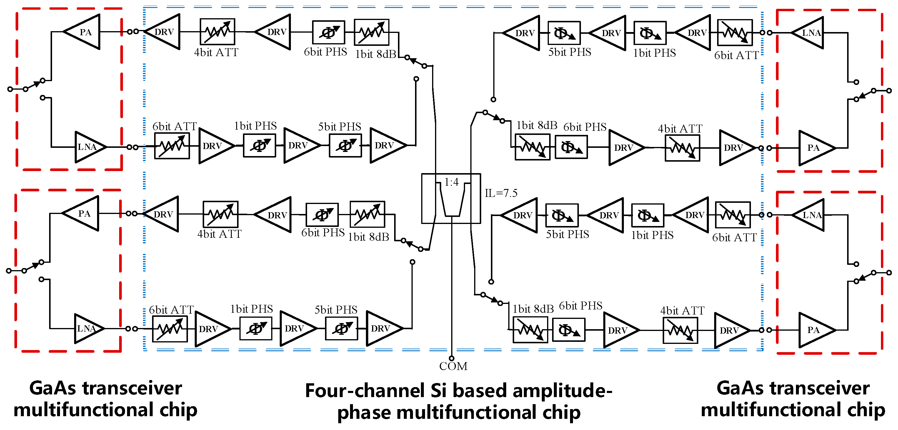
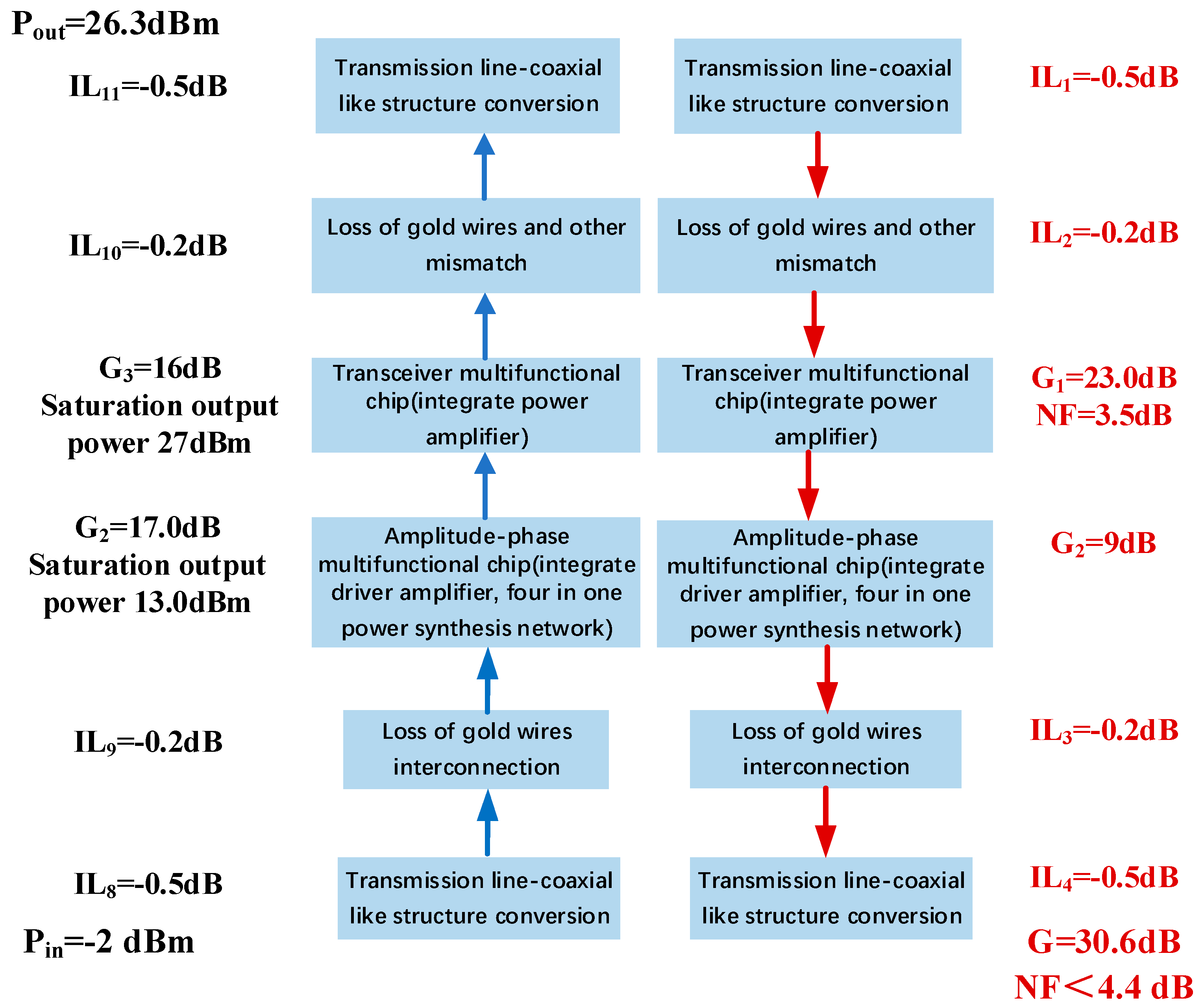
3.2. Link Design of T/R Module

The link design of T/R module needs to meet the requirements of high integration, large output power, and low loss. The functional modules of the transceiver link are divided after carefully weighing the benefits and drawbacks of Si and GaAs-based technologies in order to further enhance the integration of the T/R module. The Ka-band 0.5 W four-channel five-chip architecture, or the 1.25 chips per channel method, is employed in this article. It consists of one Si-based four-channel amplitude-phase multifunctional chip and four 0.5 W GaAs transceiver multifunctional chips. A 6-bit phase shifter, a 6-bit attenuator, a driver amplifier, and a transceiver switching interface are integrated inside each channel of the four-channel Si-based amplitude-phase multifunctional chip, as seen in Figure 2. A power amplifier, a low-noise receiving amplifier, and a transceiver switch are all internally integrated within the GaAs transceiver multifunctional device.
The GaAs transceiver multifunctional chip uses a two-stage amplification structure for its power amplifier, and a four-stage amplification and five-stage matching structure for its low-noise amplifier, which incorporates feedback networks. In order to increase the low-noise amplifier’s stability, feedback networks are also added at the input and output ends of all stages of amplification. At the input stage, noise-coefficient matching is utilized to obtain good noise factors. The transceiver switch adopts a single pole double throw switch structure. The traditional Wilkinson power divider model is utilized by the four-channel Si-based amplitude-phase multifunctional power divider, which has an insertion loss of roughly 2 dB (not counting the 6 dB distribution loss). In order to improve channel isolation and make it easier to accurately calibrate the amplitude and phase of phased array antenna channels, the switch employs a single-pole three-throw switch, which has three states: transmission, reception, and load. Drive amplifiers 2 and 3 use an RC negative feedback structure to ensure a large output power, while amplifier 5 uses a two-stage amplification structure and negative feedback to achieve a high gain, while ensuring output power. Drive amplifiers 1 and 4 adopt a traditional amplifier structure due to their small input power. For the purpose of increasing the input P-1dB, the receiving phase shifter has a passive phase shifter structure, with a large displacement phase loss of roughly 3 dB and a small displacement phase loss of about 9.5 dB The transmission phase shifter adopts an active phase shifter structure to reduce the size, with a loss of approximately 2.5 dB. The attenuator adopts a traditional single-ended structure and adds parallel capacitors for phase compensation. The receiving large-bit attenuation of 16 dB is achieved by cascading two 8 dB attenuation circuits. Both chips are internally integrated with active bias, eliminating the need for additional power modulation circuits, which can save on the number of peripheral devices and simplify the assembly and production.
This design uses Si-based technology to achieve low-power and small-size amplitude-phase control and power management circuits, as well as GaAs technology to achieve excellent amplifier output power, efficiency, and noise factor.
Compared with single-chip integrated architecture, the discrete 1.25-chip architecture can fully exploit the advantages of various process technologies, effectively balancing integration, process feasibility, functionality, and performance. When it comes to large-scale and affordable production, the discrete 1.25-chip architecture is superior to the multi-chip discrete architecture because it can significantly improve integration, simplify the T/R module layout design, streamline the production and assembly process, and guarantee amplitude and phase consistency across channels. The discrete 1.25 chip architecture achieves a high performance, high integration, and good process implementation of the T/R module. The four-channel amplitude-phase multifunctional chip adopts the 55 nm Si CMOS technique, with a size of 3.50 × 5.00 × 0.10 mm, while the transceiver multifunctional chip uses a 0.25 μm GaAs p-type high-electron mobility transistor (pHEMT) technique, measuring 2.42 mm × 1.85 mm × 0.10 mm.
Based on the above four-channel and five-chip T/R chip architecture, a device-based four-channel T/R module is constructed, consisting of one Si-based amplitude-phase multifunctional chip, four GaAs transceiver multifunctional chips, and a passive conversion structure. Under the guidance of wave control signals, each T/R channel is capable of independently achieving receiving phase shift and attenuation, transmission phase shift, and receiving/transmission/load state switching. Figure 3 displays the indication allocation and link design. IL, NF, G, Pin, and Pout denote insertion loss, noise factor, gain, input power, and output power, respectively. It can be observed that the active gain of the receiving channel is greater than 30 dB, and the noise factor is less than 4.4 dB. The transmission channel’s saturated output power is higher than 26 dBm.
The amplitude-phase multifunctional chip and transceiver multifunctional chip of the T/R module described in the paper are placed in the reserved slots of the LTCC multilayer substrate, and the LTCC substrate multilayer wiring provides electrical interconnection, heat dissipation channels, and mechanical support. The LTCC multilayer substrate material is FST07, with a relative dielectric constant of 6.6 and a loss angle tangent of 0.002. There are fifteen LTCC layers in total, and each layer is 96 μm thick, as shown in Figure 4a. Silver-based slurry is utilized on ceramic substrates to produce high-precision, high-density microwave and low-frequency circuits. The second layer of the LTCC substrate is a large-area grounding pad. Punch the substrate from the surface layer to the second layer and then stack and press them to form a blind cavity. Place the four-channel T/R sleeve on the large area grounding pad in the cavity, so that the chips and the surface pads are basically on the same horizontal plane, facilitating bonding operations and shortening the length of gold wires. The conductors from the third-to-fifth layers of the substrate form the power and control circuits, connected to the surface and bottom conductors through the conductor through holes, providing power and control signals for the four-channel T/R chips. The sixth-to-fifteenth layers of the LTCC substrate are Ka-band signal horizontal transmission layers, where the sixth layer is the upper ground layer for the stripline, isolating the microwave signal layer and the low-frequency signal layer to enhance shielding. The eleventh layer is the Ka-band signal horizontal transmission line layer. The bottom layer serves as the lower ground plane for the stripline, and the sixth ground plane is connected to the bottom ground plane through the conductor through holes arranged on both sides of the stripline, playing a shielding role. A Ka-band signal, power supply, and control signal pad are also located on the bottom layer. The BGA solder balls implanted on the bottom pad are interconnected with external circuit boards to achieve both high- and low-frequency signal input and output. The last surface coating layer is an electroless Ni/Pd/Au film that is utilized for bonding pads for bare chips, surface-mounted resistive and capacitive devices, wire-bonding connecting pads, and bonding pads for metal frame packaging. Figure 4b exhibits the printing and punching layout for each layer.

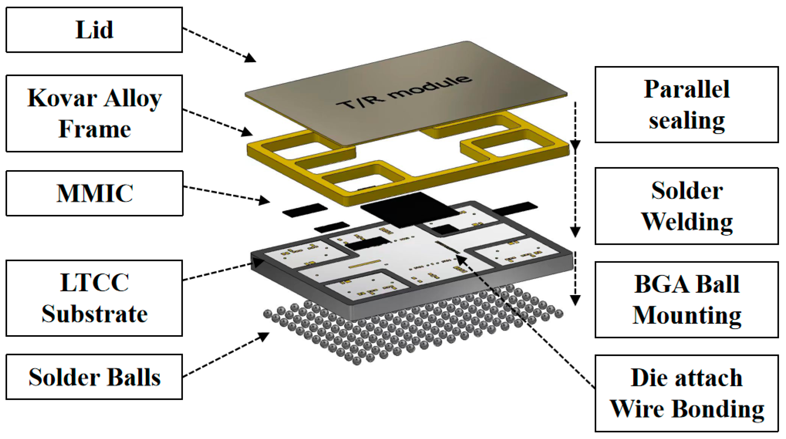
3.3. Device-Based Packaging Design

The four-channel T/R module adopts device-based packaging. As shown in Figure 5, the device-based T/R module uses an LTCC substrate as the packaging substrate, and the 4J29 Kovar alloy with a similar thermal expansion coefficient to the LTCC substrate within a wide temperature range (−70~500 °C) is selected as the enclosure material. The electrical interconnection interface adopts the BGA form, and the LTCC substrate is coated with Ni/Pd/Au film on the surface and then welded with gold tin alloy solder to form an airtight packaging for the metal enclosure and cover plate. The device-based T/R module achieves functional integration of mechanical support, 3D wiring, and heat dissipation by utilizing the dielectric characteristics, mechanical strength, thermal conductivity, and sealing qualities of the ceramic materials themselves. The components are interconnected with external circuits through a surface mount assembly, saving the size and weight of high- and low-frequency connectors and improving the integration of phased array antenna systems. The silver slurry is used as the conductor of 3D wiring, and the surface is coated with an electroless Ni/Pd/Au-plating process to meet the assembly requirements of various components and greatly reduce the process cost.

4. Optimization of Interconnection Structure

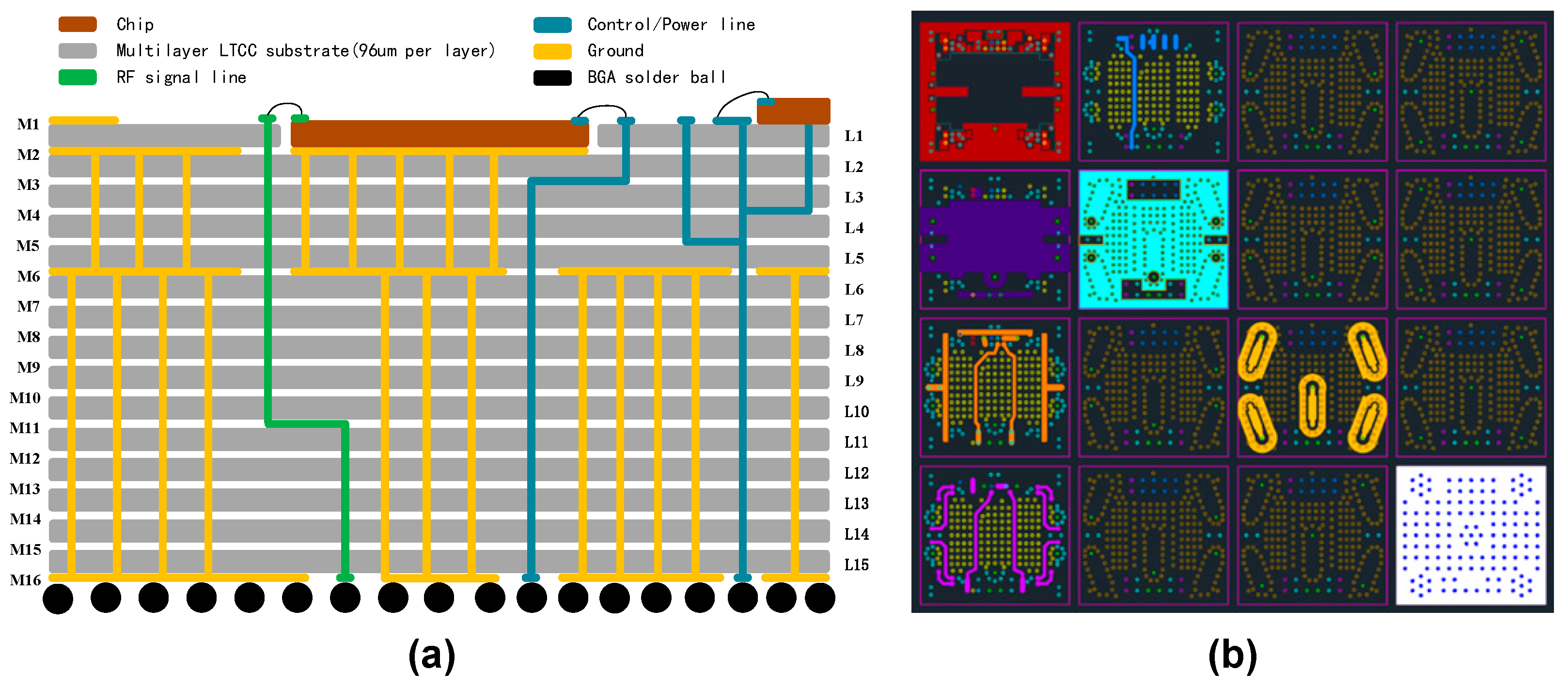
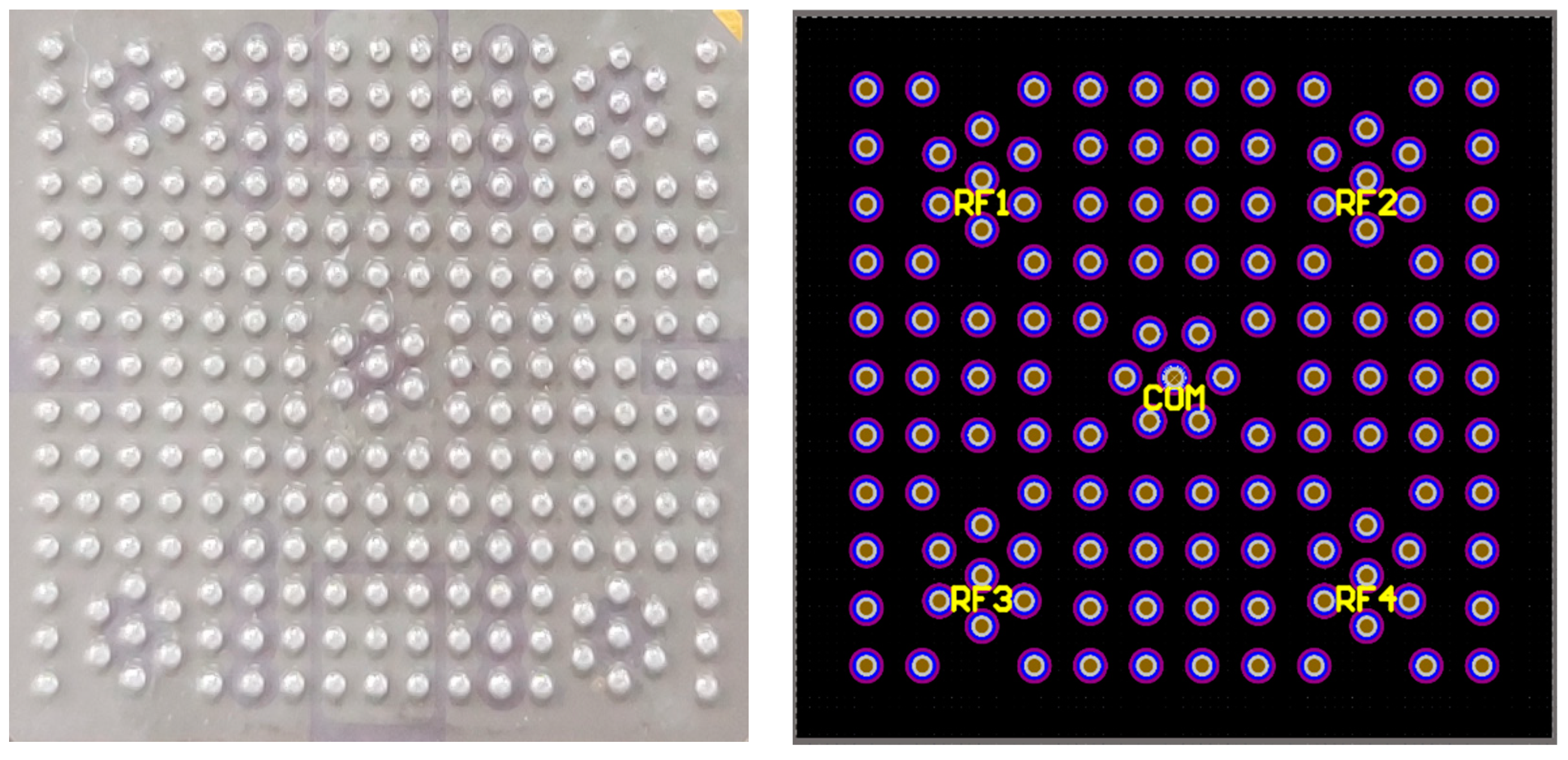
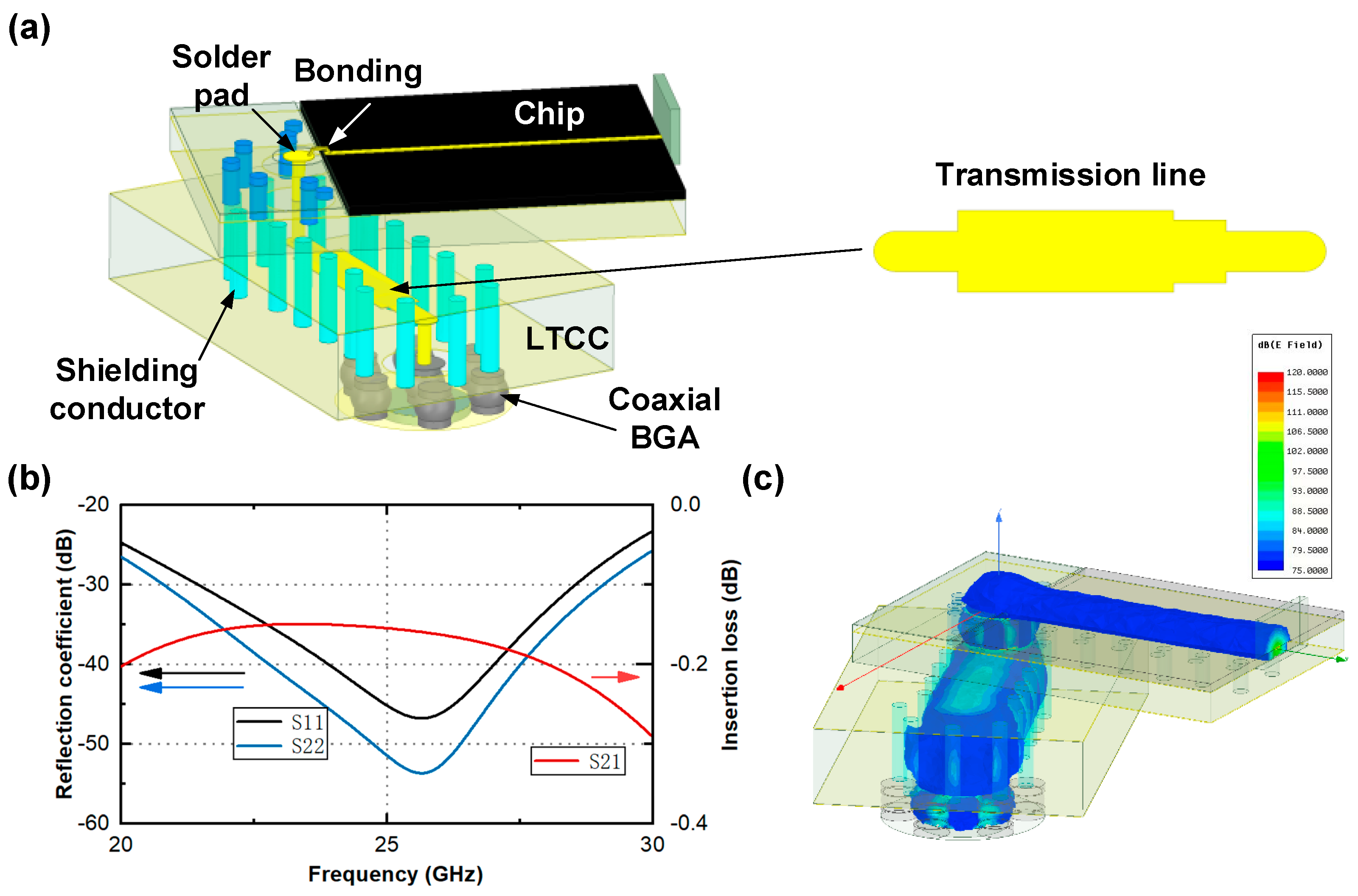
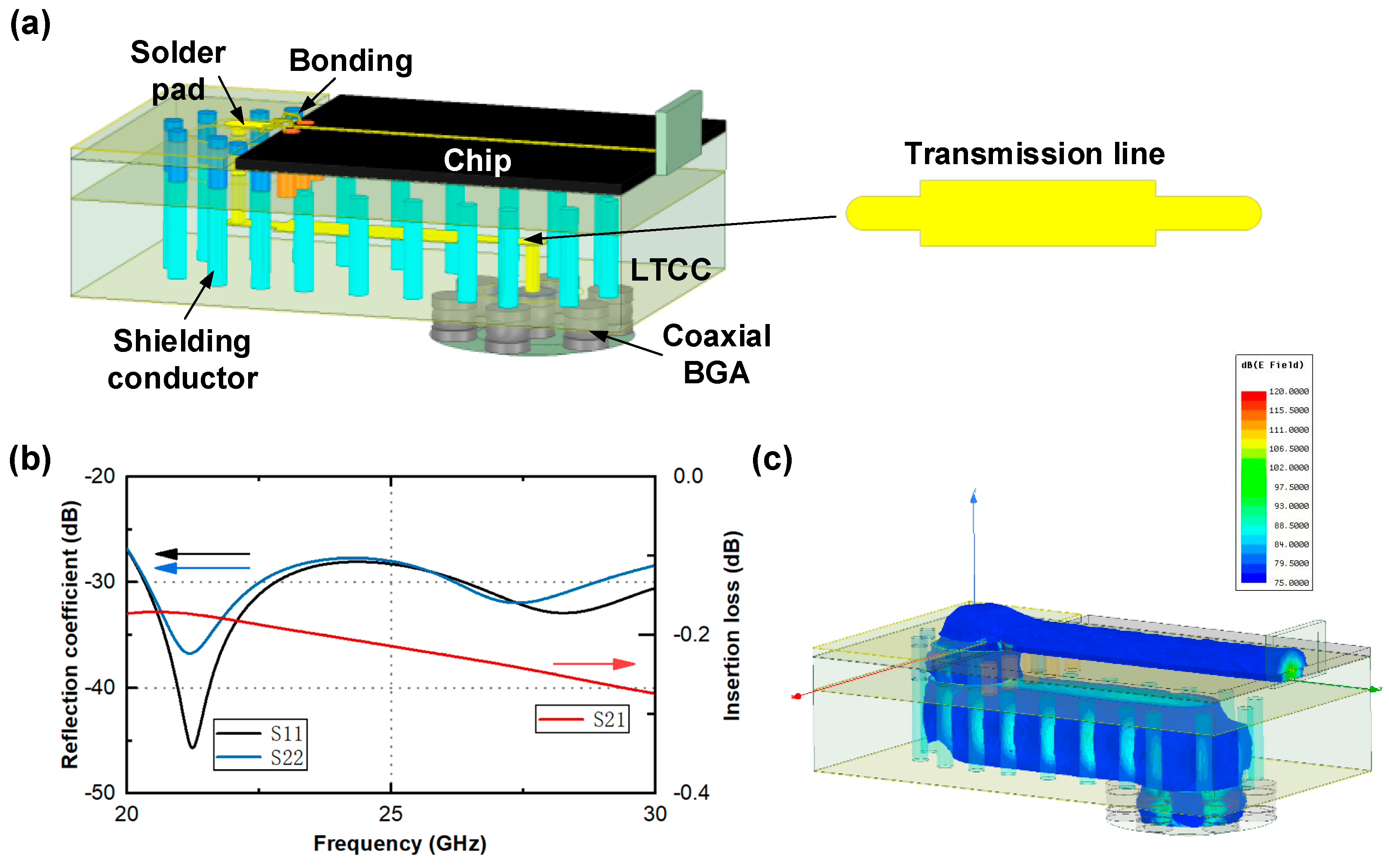
4.1. Design of Device Based Interconnection Interface

When mounting and interconnecting components of this device-based T/R module, the interconnection is required to occupy a small area of the multifunctional board, have low millimeter-wave RF transmission loss, and have good isolation inside and among modules. In order to satisfy the high-performance and low-profile connecting requirements of phased array antenna microsystems, the T/R module referred to in this article uses a BGA as its interconnection interface for signal transmission, regardless of frequency.
BGA packaging can accomplish high-density RF and low-frequency connections by using solder balls in place of conventional metal leads or connectors. The balls are arranged in a two-dimensional array on the back of the packing substrate. Its short signal transmission path and minimal cable parasitic impact help to achieve a good transmission performance. BGA solder balls can be arranged in a coaxial-like structure, as seen in Figure 6, with a solder ball located in the center to replace the inner conductor of the coaxial line, and a circle of solder balls on the periphery to replace the grounding shielding layer of the standard coaxial line. The coaxial-structure BGA interface can achieve great shielding of electromagnetic wave signals in the Ka-band range, as shown in Figure 6, thereby achieving high isolation between RF ports. Figure 7 presents HFSS models comparing electric fields, as well as magnetic field distributions of the quasi-coaxial structure and coaxial structure, showing excellent and similar performance in confining the electromagnetic field inside for both structures.

4.2. Design of RF Full-Path Interconnection

In the article, the transceiver multifunctional chip is connected to LTCC through wire bonding after being pasted to a large-area solder pad, using conductive adhesive. The millimeter-wave signal is transmitted from the surface to the BGA solder ball output at the bottom of the LTCC substrate in three-dimensional form. It is necessary to optimize the design of the millimeter-wave signal full path interconnection structure of “chip–gold wire–LTCC surface–vertical interconnection–stripline–vertical interconnection–BGA solder ball”.
The high-frequency structural simulator (HFSS) model’s simulation results demonstrate that an impedance mismatch arises from the discontinuous structure between the bonding wire and the pad when chips are directly bonded through gold wire to the inner conductor of a vertical coaxial structure. This leads to a notable decline in the performance of signal transmission. Zin is also in a state of impedance mismatch. Since this degradation is more noticeable at higher frequencies, the transmission performance must be improved on successive striplines by conducting impedance matching.
As illustrated in Figure 8a, a model of the RF path “chip–gold wire–coaxial structure–stripline–coaxial structure–BGA solder ball” was established for the device-based T/R module in order to optimize the interconnection structure. This was achieved by adding multiple matching structures with varying line widths and lengths to the stripline.
Figure 8b presents the simulation findings. It can be seen that, in the wide frequency range of 20–30 GH, the reflection coefficient is less than −20 dB, and the transmission loss is less than 0.4 dB. The electric field distribution results are shown in Figure 8c and show that the electromagnetic field is confined to the transmission path, indicating that the interconnection structure has an excellent transmission performance.
The difference between the RF input channel and output interface of the device-based T/R module is that the overall port of the amplitude-phase multifunctional chip on the RF input channel has larger wiring space, and the LTCC substrate’s surface can accommodate the addition of a coplanar waveguide. The HFSS simulation model is shown in Figure 9a.
Simulation results are shown in Figure 9b, where the reflection coefficient is less than −20 dB and the transmission loss is less than 0.4 dB in the wide frequency range of 20–30 GHz. The electric field simulation model is shown in Figure 9c, presenting that the electromagnetic field is also well confined to the transmission path.

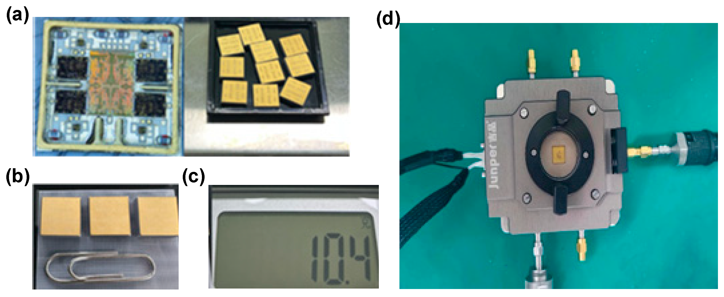
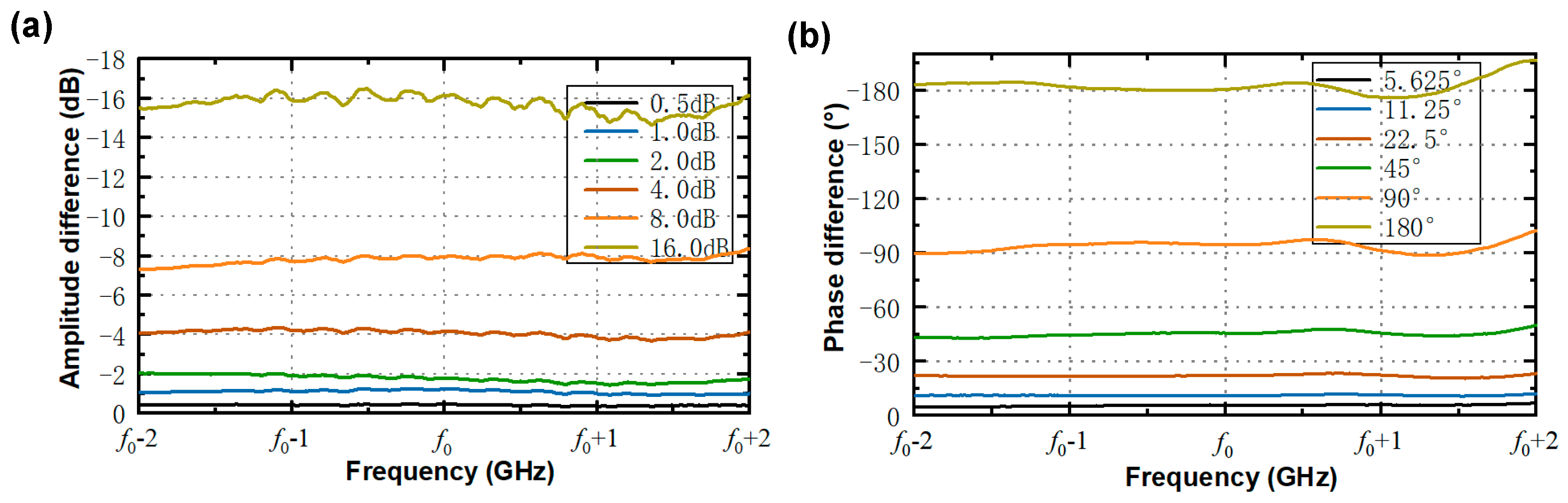
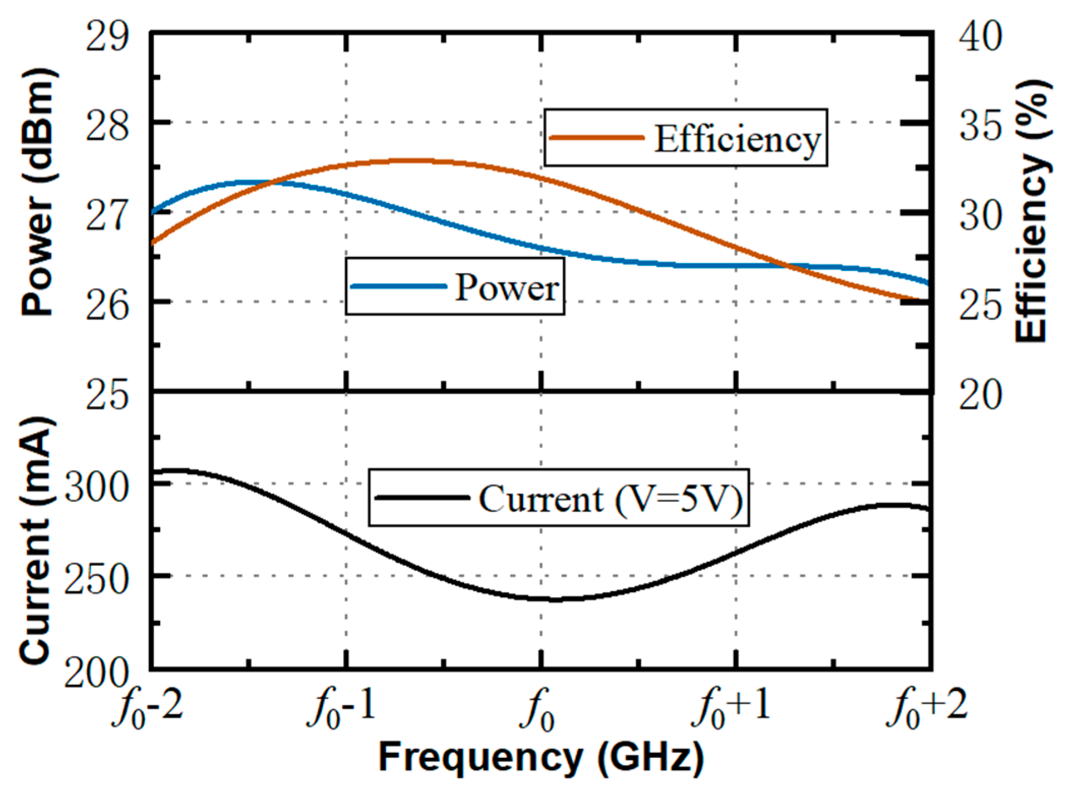
5. Testing the Key Parameters of the Device-Based T/R Module

Figure 10 displays the device-based T/R module’s photo and testing environment. The module weighs 1 g and has overall dimensions of 10.8 × 10 × 3 mm. The testing results are summarized in Table 1.
To measure the receiving performance of the module’s single channel, put the other three channels into receiving standby mode, meaning that the receiving amplifier is turned off; and put the RF port into load mode.
The results of the single-channel ground-state receiving test are shown in Figure 11, and it can be seen that the in-band receiving gain exceeds 26 dB. Considering that the four-in-one power synthesis network introduces an additional insertion loss of about 6 dB, the in-band receiving gain for a single channel ground state is greater than 33 dB, which matches the predicted value 30.6 dB in Figure 3 well. The in-band noise factor is less than 4.4 dB, agreeing with the value 4.4 dB put forward in Figure 3. The test results meet our expectations.
The test results of the 6-bit attenuator and phaser are shown in Figure 12. The amplitude or phase measured following a particular amplitude modulation (a) or phase modulation (b) on the basis of a single-channel ground state is represented by each curve in Figure 12, with the particular amplitude modulation or frequency modulation value shown on the label of the curve. It is shown that the test results agree well with the set values within a wide band range (f0 − 2~f0 + 2 GHz, f0 = 24), verifying that this T/R module has stable and accurate attenuation and phase-shifting effects.
Set the RF port to the load state and the other three channels to the transmitting standby state—that is, with the transmitting amplifier turned off—when evaluating the transmission performance of the module’s single channel.
The test results of the single-channel transmission output power and current are shown in Figure 13. It can be seen that the output power of the device-based four-channel T/R module within a single channel 4 G bandwidth is greater than 26.2 dBm, which is superior, as seen from the comparison in Table 1. Additionally, the emission current, which has a maximum value of 300 mA and is related to efficiency at different frequencies, has an efficiency of more than 25%. The test results comply with the design values in Figure 3, considering a 6 dB insertion loss induced by the one-to-four power divider.

6. Conclusions

This work offers a device-based four-channel T/R module scheme based on a multi-material heterogeneous integration architecture incorporating Si/GaAs/LTCC to meet the demand for the devitalization of T/R modules in the millimeter-wave phased array antenna microsystem architecture design. By designing the chip architecture, connections, wiring, packaging, interfaces for interconnection, and full path interconnection, millimeter-wave four channel T/R modules are devitalized, and their critical parameters are tested. This module breaks through the device-based packaging of millimeter-wave signal full-path three-dimensional transmission interconnection, achieving a four-channel module overall size of 10.8 mm × 10 mm × 3 mm, weight of 1 g, single-channel transmission output power ≥ 26 dBm, efficiency ≥ 25%, and noise factor ≤ 4.4 dB, meeting the high-performance T/R module requirements of Ka-band phased array antenna microsystems for high dynamic platform communication. When compared to other T/R modules, this one has advantages like simple integration, a straightforward interface for connecting, and a high output power per unit volume.
With its low profile, high power, and low loss, this research offers a practical and workable design example for a device-based multichannel T/R module design. It has a wide range of applications and enormous potential, but more research and development are required.

Author Contributions

Methodology, Q.Z.; software, Z.C.; validation, M.H., S.W. and X.L.; formal analysis, Q.Z.; investigation, X.L.; resources, H.X.; data curation, X.L.; writing—original draft preparation, Q.Z. and X.L.; writing—review and editing, Q.Z.; project administration, H.X.; funding acquisition, H.X. All authors have read and agreed to the published version of the manuscript.

Funding

This research was funded the Aerospace Information Research Institute, Chinese Academy of Sciences, grant numbers E1Z221030F, and partly by the Scientific and Technological Innovation Foundation of Shunde Graduate School, USTB (BK22BF002).

Data Availability Statement

Data are contained within the article.

Conflicts of Interest

The authors declare no conflict of interest.

References

  1. Han, G.; Du, B.; Wu, W.; Yang, B. A Novel Hybrid Phased Array Antenna for Satellite Communication on-the-Move in Ku-band. IEEE Trans. Antennas Propag. 2015, 63, 1375–1383. [Google Scholar] [CrossRef]
  2. Alakija, C.; Stapleton, S.P. A mobile base station phased array antenna. In Proceedings of the 1992 IEEE International Conference on Selected Topics in Wireless Communications, Vancouver, BC, Canada, 25–26 June 1992. [Google Scholar]
  3. Hu, R.; Li, X.; Deng, J.; Zhou, J.; Dong, S.; Liu, L.; MA, W. Research on the Architecture of Phased Array Antenna of LEO Communication Satellites Based on Hybrid Beamforming. Space-Integr.-Ground Inf. Netw. 2021, 2, 8. [Google Scholar]
  4. Hong, W.; Jiang, Z.H.; Yu, C.; Zhou, J.; Chen, P.; Yu, Z.; Zhang, H.; Yang, B.; Pang, X.; Jiang, M.; et al. Multibeam Antenna Technologies for 5G Wireless Communications. IEEE Trans. Antennas Propag. 2017, 65, 6231–6249. [Google Scholar] [CrossRef]
  5. Gan, Z.; Zhang, G. Current development of satellite communications technology. J. Commun. 2006, 8, 8. [Google Scholar]
  6. Yang, W. Array Antenna Technology in Mobile Communications; Beijing Jiaotong University Press: Beijing, China, 2005. [Google Scholar]
  7. Bil, R.; Holpp, W. Modern phased array radar systems in Germany. In Proceedings of the 2016 IEEE International Symposium on Phased Array Systems and Technology (PAST), Waltham, MA, USA, 18–21 October 2016; pp. 1–7. [Google Scholar]
  8. Morrison, G.D.; McLachlan, A.D.; Kinghorn, A.M. “Tile”-based airborne phased array radar systems. In Proceedings of the International Conference on Radar Systems (Radar 2017), Belfast, UK, 23–26 October 2017; pp. 1–4. [Google Scholar]
  9. Pirkl, M.; Holpp, W. From research to application: How phased array radars conquered the real world. In Proceedings of the 2013 14th International Radar Symposium (IRS), Dresden, Germany, 19–21 June 2013; pp. 17–22. [Google Scholar]
  10. Brookner, E. Advances and breakthroughs in radars and phased-arrays. In Proceedings of the 2016 CIE International Conference on Radar (RADAR), Guangzhou, China, 10–13 October 2016; pp. 1–9. [Google Scholar]
  11. Lambard, T.; Lafond, O.; Himdi, M.; Jeuland, H.; Bolioli, S.; Coq, L.L. Ka-Band Phased Array Antenna for High-Data-Rate SATCOM. IEEE Antennas Wirel. Propag. Lett. 2012, 11, 256–259. [Google Scholar] [CrossRef]
  12. Lai, Q.; Li, P.; Jin, M.; Gao, C.; Yuan, T. A mm-wave multiple-beam phased array breadboard for GEO-LEO inter-satellite links. In Proceedings of the 2014 IEEE MTT-S International Microwave Symposium (IMS2014), Tampa, FL, USA, 1–6 June 2014; pp. 1–3. [Google Scholar]
  13. Cooley, M. Phased Array Fed Reflector (PAFR) antenna architectures for space-based sensors. In Proceedings of the 2015 IEEE Aerospace Conference, Big Sky, MT, USA, 7–14 March 2015; pp. 1–11. [Google Scholar]
  14. Ivanov, A.; Teplyakov, V.; Kalinin, V. Mobile communication system with a hybrid phased array antenna system. In Proceedings of the 2015 IEEE East-West Design & Test Symposium (EWDTS), Batumi, Georgia, 26–29 September 2015; pp. 1–4. [Google Scholar]
  15. Lee, W.-B.; Im, C.-S.; Zhou, C.; Bhandari, B.; Choi, D.-Y.; Lee, S.S. Metasurface doublet-integrated bidirectional grating antenna enabling enhanced wavelength-tuned beam steering. Photonics Res. 2022, 10, 248–255. [Google Scholar] [CrossRef]
  16. Li, Y.; Chen, B.; Na, Q.; Xie, Q.; Song, J. Wide-steering-angle high-resolution optical phased array. Photonics Res. 2021, 9, 2511–2518. [Google Scholar] [CrossRef]
  17. Ginel-Moreno, P.; Hadij-ElHouati, A.; Sánchez-Postigo, A.; Wangüemert-Pérez, J.G.; Molina-Fernández, Í.; Schmid, J.H.; Cheben, P.; Ortega-Moñux, A. On-Chip Metamaterial Antenna Array with Distributed Bragg Deflector for Generation of Collimated Steerable Beams. Laser Photonics Rev. 2022, 16, 2200164. [Google Scholar] [CrossRef]
  18. Bai, X.; Zhang, F.; Sun, L.; Cao, A.; Wang, X.; Kong, F.; Zhang, J.; He, C.; Jin, R.; Zhu, W.; et al. Cuiradiation-type programmable metasurface for direct manipulation of electromagnetic emission. Laser Photonics Rev. 2022, 16, 2200140. [Google Scholar] [CrossRef]
  19. Xue, J. Fundamentals of Millimeter-Wave Engineering; Harbin Institute of Technology Press: Shenzhen, China, 2004. [Google Scholar]
  20. Xiang, J.; Zhang, M. Millimeter-Wave Radar and Its Applications; National Defense Industry Press: Beijing, China, 2005. [Google Scholar]
  21. Ruan, C. Millimeter-Wave Theory and Technology; University of Electronic Science and Technology of China Press: Chengdu, China, 2001. [Google Scholar]
  22. Qi, S.; He, Z. Study of Millimeter Wave Phased Array Antenna. Shipboard Electron. Countermeas. 2004, 27, 14–16. [Google Scholar]
  23. Sadhu, B.; Gu, X.; Valdes-Garcia, A. The More (Antennas), the Merrier: A Survey of Silicon-Based mm-Wave Phased Arrays Using Multi-IC Scaling. IEEE Microw. Mag. 2019, 20, 32–50. [Google Scholar] [CrossRef]
  24. Li, S. Ka Band Delay-Line Components Based on LTCC Technology; University of Electronic Science and Technology of China: Chengdu, China, 2014. [Google Scholar]
  25. Liu, X.; Hao, J. Design of Ka-band Multi-channel transmitting. Shipboard Electron. Countermeas. 2015, 38, 210–219. [Google Scholar]
  26. Guo, F.; Jiang, W.; Wang, Z. A Ka-band transceiver based on LTCC technology. In Proceedings of the 2013 International Workshop on Microwave and Millimeter Wave Circuits and System Technology, Chengdu, China, 24–25 October 2013. [Google Scholar]
  27. Wang, Y. Research on a Ka Band T/R Module Array Based on LTCC Technolog; Beijing Institute of Technology: Beijing, China, 2016. [Google Scholar]
  28. Wan, T.; Wang, Y. Miniaturization and multilayer for 3-D T/R module. J. Terahertz Sci. Electron. Inf. Technol. 2016, 14, 758–762. [Google Scholar]
  29. Chu, C.Y.; Tseng, S.T.; Gao, J.Z.; Chen, Y.P.; Chang, Y.C.; Tseng, C.W.; Huang, T.Y.; Hu, B.S.; Su, B.; Chu, T.S.; et al. A fully-integrated Ka-band 4TX/4RX phased-array transceiver IC in 65nm CMOS. In Proceedings of the 2016 IEEE International Symposium on Radio-Frequency Integration Technology (RFIT), Taipei, Taiwan, 24–26 August 2016. [Google Scholar]
  30. Cui, L.; Zhang, Z.; Hu, Y.; Ji, L. Packaging Technology for Ka-band T/R Modules Based on LTCC Thick-thin Film Hybrid Substrate. Mod. Radar 2017, 9, 86–89. [Google Scholar]
  31. He, Q.Q.; Ding, S.; Xing, C.; Chen, J.Q.; Yang, G.Q.; Wang, B.Z. Research on Structurally Integrated Phased Array for Wireless Communications. IEEE Access 2020, 8, 52359–52369. [Google Scholar] [CrossRef]
  32. Sun, L. A Review of Antenna-in-package Technology for Millimeter-wave Phased Array Antennas. Mod. Radar 2020, 42. [Google Scholar]
  33. Liu, X. A novel airproof miniaturized millimeter-wave TR module. Electron. Test. 2021, 20. [Google Scholar]
  34. Yang, D.; Zhao, Y. A Ka Band Four-Channel Short Brick-Type 3D Integrated T/R Microsystem with Silicon-Based MEMS Technology. IC Des. Appl. 2023, 48, 506–511. [Google Scholar] [CrossRef]
  35. Lu, J.G.; Wang, Y. From active phased array antenna to antenna array microsystem in post-Moore era. Sci. Sin. Inf. 2020, 50, 19. [Google Scholar]
  36. Herd, J.S.; Conway, M.D. The Evolution to Modern Phased Array Architectures. Proc. IEEE 2016, 104, 519–529. [Google Scholar] [CrossRef]
Figure 1. EIRP of phased array antenna with 16 (a) and 1024 (b) phased-array elements. (c) The EIRP grows as N × N, while (d) the beamwidth reduces as N versus the number of phased-array elements in a square array. Images reproduced from the literature [23].
Electronics 13 00204 g001
Figure 2. Schematic block diagram of Ka-band 0.5 W four-channel T/R module.
Electronics 13 00204 g002
Figure 3. T/R module transmitting and receiving link design and indicator allocation.
Electronics 13 00204 g003
Figure 4. Schematic and layout of multilayer LTCC substrate: (a) schematic of multilayer LTCC substrate and (b) layout of LTCC substrate.
Electronics 13 00204 g004
Figure 5. Schematic of tile four-channel T/R module.
Electronics 13 00204 g005
Figure 6. Device-based four-channel T/R module BGA interconnection interface, applying coaxial like structure.
Electronics 13 00204 g006
Figure 7. Comparison of electromagnetic field distributions between quasi-coaxial structure and coaxial structure: (a) electric fields and (b) magnetic fields.
Electronics 13 00204 g007
Figure 8. (a) HFSS model of radio frequency output interconnection structure. (b) Simulation results of radio frequency output interconnection structure. (c) Simulation results of electric field distribution in interconnection structure.
Electronics 13 00204 g008
Figure 9. (a) HFSS model of radio frequency input interconnection structure. (b) Simulation results of tile T/R module radio frequency input interconnection structure. (c) Simulation results of electric field distribution in interconnection structure.
Electronics 13 00204 g009
Figure 10. (a) Fabricated prototype of tile T/R module. (b) Size comparison between T/R modules and a clip. (c) A T/R module weight of 10.4 g. (d) Test environment of tile T/R module.
Electronics 13 00204 g010
Figure 11. Measurement results of single-channel base-state reception.
Electronics 13 00204 g011
Figure 12. Measurement results of phase shift and attenuation. (a) amplitude modulation. (b) phase modulation.
Electronics 13 00204 g012
Figure 13. Measured results of output power, efficiency, current with single channel transmitting.
Electronics 13 00204 g013
Table 1. Research achievements of Ka-band T/R modules domestically and internationally.
TimeInstitutionModuleTechniqueSizeOutput Power (dBm)Noise Factor (dB)Other ParameterReference
2014University of Electronic Science and Technology of ChinaKa-band 6-channel switching delay line moduleLTCC84 mm × 47 mm × 15 mm\\\[24]
2015The 13th Research Institute, CETCKa-band 16-channel transmission modulePCB multilayer wiring technique and multi-chip assembly technique60 mm × 80 mm × 4.8 mm>25\Linear gain > 25 dB[25]
2015Institute of Telecommunication Satellite, CASTKa-band T/R moduleLTCC36 mm × 20 mm × l.l mm>24.6<4.2Receiving gain ~33 dB, output gain > 25 dB[26]
2016Beijing Institute of TechnologyKa-band T/R arrayLTCCSingle channel cross-section 6 mm × 25 mm>10.5<4.5\[27]
2016Xi’an Research Institute of Navigation TechnologyKu-band 3D miniaturized T/R moduleLTCC, BGA9.5 mm × 9.5 mm × 3.8 mm>24.5<3.5Receiving gain > 25 dB[28]
2016Ching-Yun ChuKa-band 4-channel T/R chip65 nm CMOS technique4 mm × 2.5 mm~18.5~4.4\[29]
2017Nanjing Research Institute of Electronics TechnologyKa-band 8-channel T/R moduleLTCC43 mm × 39.5 mm × 3.5 mm\\Return loss > 15 dB[30]
2020Southwest China Institute of Electronic TechnologyKa-band circularly polarized phased array antennaLTCC46 mm × 44 mm × 2.8 mm\\\[31]
2020Nanjing Research Institute of Electronics TechnologyKa-band 64-channel phased array antennaSilicon based packaging integration, chip embedded packaging\\\\[32]
2020Chengdu radio wave technology Co., Ltd.Ka-band 128-unit tile phased array antennaIntegrated packaging of Si-based multifunctional and GaAs transceiver chips93 mm × 93 mm × 52 mm>20<6.5\[33]
2021Aerospace Information Research Institute, Chinese Academy of SciencesKa-band 4-channel T/R moduleLTCC, BGA, multi-material heterogeneous integration10.8 mm × 10 mm × 3 mm≥26≤4.4Efficiency ≥ 25%This work
2023The 13th Research Institute, CETCKa-band 4-channel T/R moduleSilicon-based MEMs, TSV, 3D integration18 mm × 19.5 mm × 3 mm≥30≤4.6 [34]
Table 2. Comparison of phase array antenna microsystem architecture.
Integrated Architecture of Phased Array Antenna MicrosystemsRequirements for Chip IntegrationTechnique RequirementsSingle Channel Output PowerTestabilityResearch and Development CostMillion Level Batch Production Cost
Brick and wafer typeLowMetal shells with multi-chip planar packaging; high- and low-frequency cable interconnectionHighGoodLowHigh
Three-dimensional heterogeneous flat plate typeRelatively highCeramic, silicon, and glass adapter plates; embedded packaging; hybrid multilayer boards; and surface assemblyRelatively highRelatively goodRelatively lowRelatively low
Silicon based RF circuit integrationHighSOC chips and their packaging techniques based on Si Complementary Metal Oxide Semiconductor (CMOS) and SiGe BiCMOS LowRelatively goodHighLow
heterogeneous integrationHighSi CMOS and SiGe BiCMOS wafer-based technique; direct heterojunction of silicon compoundsLowBadVery highLow
2016Xi’an Research Institute of Navigation TechnologyKu-band 3D miniaturized T/R moduleLTCC, Ball Grid Array (BGA)9.5 mm × 9.5 mm × 3.8 mmTransmission output power > 24.5 dBm, receiver gain > 25 dB, and receiving noise factor < 3.5 dB[17]
Disclaimer/Publisher’s Note: The statements, opinions and data contained in all publications are solely those of the individual author(s) and contributor(s) and not of MDPI and/or the editor(s). MDPI and/or the editor(s) disclaim responsibility for any injury to people or property resulting from any ideas, methods, instructions or products referred to in the content.

