Abstract
An accurate analysis method for an LLC resonant converter and a time-domain analysis (TDA)-based voltage gain curve derivation algorithm are proposed in this paper. When applied to an LLC resonant converter, the TDA method can obtain high-accuracy current and voltage waveforms by solving nonlinear equations for circuit parameters through operation-mode analysis. An LLC resonant converter operating mode classification algorithm was proposed based on the results of this analysis. The circuit voltage and current values in the steady state were quickly and precisely derived using this algorithm. An accurate power-loss analysis is required to design a high-efficiency converter. Therefore, TDA is a powerful tool for designing an LLC resonant network. The proposed TDA-based LLC resonant converter analysis and voltage gain curve derivation algorithm provides high-accuracy voltage, current value estimation and voltage gain curves for all switching-frequency ranges. The effectiveness of the proposed algorithm is verified using a 500 W LLC resonant converter prototype experiment.
1. Introduction
High-power density DC–DC converters that use wide-bandgap (WBG) power semiconductors are required in the modern power electronics industry [1]. High power density can be achieved by reducing the size of passive components by increasing switching frequency; however, this approach increases the switching loss. An LLC resonant half-bridge converter is shown in Figure 1, wherein soft switching is achieved over the entire load range and it shows advantages of minimizing loss despite increasing the switching frequency. Therefore, LLC resonant half-bridge converters are widely used in applications requiring high efficiency and density, such as in electric vehicles, LED drivers, and solar power generation [2,3]. Improving the design accuracy is important to increase the utilization of the LLC resonant converter and maximize its advantages. To this end, the accurate operation and loss analysis of the LLC resonant converter needs to be prioritized.
Figure 1.
Half−bridge LLC resonant converter topology.
Accordingly, various analysis techniques for the accurate operation and loss analysis of the LLC resonant converter have been reported. For example, a first-harmonic approximation (FHA) analysis method that only considers the fundamental sinusoidal components of the circuit voltage and current was proposed to simplify the analysis and design of the LLC resonant converter [4]. The FHA technique is the commonly used analysis method in the frequency domain. It is used as a basic analysis method because its formula is intuitive and simple. The FHA technique only considers the basic sine wave components of the converter’s current and voltage, and therefore, it has a disadvantage that significant errors can occur with the actual result because the harmonic effect is not considered [5,6].
To solve these problems, an improved FHA technique that reflects and analyzes harmonic components in addition to the basic sine wave for the LLC resonant converter was proposed [4]. This technique performs mathematical modeling based on current and voltage waveforms while considering harmonics, which enables us to derive accurate current values. However, accuracy cannot be guaranteed under all conditions because the analysis error of this method increases depending on the LLC resonant converter design specification. An analysis technique with higher accuracy was proposed by considering the resonant factor and load factor according to the design specifications of the LLC resonant converter [7,8]. This technique helped derive a voltage gain curve for designing a high-efficiency LLC resonant converter and accurate values of voltage and current. However, the application range of the technique is limited to the region below the resonant frequency because of the increase in the estimation error when the switching frequency is above the resonant frequency.
Therefore, in order to solve these limitations of the frequency-based analysis method, a time-domain-based LLC resonant converter analysis method has been proposed [9]. In [9], a method of deriving the voltage and current in the resonant network using a time-based nonlinear equation below the resonant frequency, at the resonant frequency point, and above the resonant frequency is proposed. However, this method only classifies three types of the LLC operation mode (1. < , 2. = , 3. > ), so the accuracy of estimating voltage and current value is not high. To solve this problem, a time-domain analysis (TDA)-based LLC resonant converter analysis technique that can estimate the magnitude of voltage and current with high accuracy regardless of design conditions such as operating frequency and magnitude of the load and a voltage gain derivation algorithm are proposed in this paper. To this end, the concept of subinterval P, N, O, which is defined according to the magnitude of the voltage applied to the magnetizing inductor and combination of those subintervals considering the boundary of each operation mode, is suggested, and the circuit voltage and current magnitudes are estimated with high accuracy based on these concepts. The analytical solution for the circuit variables is derived based on nonlinear equations. This increases the complexity of the equations, which makes it necessary to use software for performing numerical analysis to solve these equations. Therefore, the equations reported in this paper and the LLC resonant converter operation mode analysis are performed using numerical analysis software. The effectiveness of the TDA-based analysis technique and voltage curve derivation algorithm are verified through comparison with experimental results based on the 500 W LLC resonant converter prototype.
The remainder of this paper is organized as follows: In Section 2, the operation mode analysis of the LLC resonant converter is conducted using a TDA-based analysis technique. Section 3 introduces an algorithm that can classify each operation mode and proposes an algorithm for deriving a voltage gain curve based on this algorithm. In Section 4, the effectiveness of the proposed technique is verified through TDA-based analyses and experiments. Finally, Section 5 presents the overall summary and conclusions of this study.
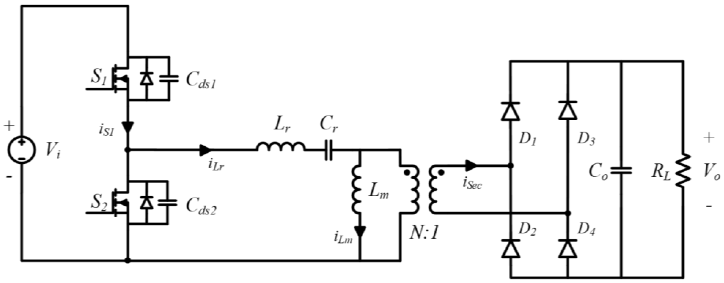
2. TDA-Based LLC Resonant Converter Analysis Technique
2.1. Operation Mode Analysis of LLC Resonant Converter
The operation state of an LLC resonant converter can be divided into three states based on the state during the half-cycle of switching. Figure 2 shows the equivalent circuits in different operating states [6]. Subinterval P in Figure 2a represents the interval at which the voltage across the magnetizing inductor of the LLC resonant converter is clamped to the positive output voltage . By applying Kirchhoff’s voltage law (KVL) to the equivalent circuit in subinterval P, the differential equation can be expressed as
Figure 2.
Equivalent circuit for each operating state of the LLC resonant converter: (a) P subinterval, (b) N subinterval, (c) O subinterval.
When the general solution of Equation (1) is obtained, the resonant capacitor Cr voltage and the resonant inductor Lr current can be, respectively, expressed as
Here, k1 and k2 represent the coefficients determined by the initial conditions of the circuit, and the series resonance angular frequency ωr is expressed as
Equation (5) can be derived by applying the KVL theory to Figure 2b, and it derives the nonlinear equation of the N subinterval. When the general solution of Equation (5) is obtained, it can be, respectively, expressed for the resonant capacitor Cr voltage and resonant inductor Lr current as
Here, k3 and k4 are coefficients determined by the initial conditions of the circuit.
In addition, subinterval O in Figure 2c represents the interval where the voltage across the magnetizing inductor Lm is not clamped to the output voltage. Applying KVL to the equivalent circuit in subinterval O results in
When the general solution of Equation (8) is obtained, it can be, respectively, expressed for the resonant capacitor Cr voltage and resonant inductor Lr current as
Here, k5 and k6 represent coefficients determined by the initial conditions of the circuit. The parallel resonance angular frequency ωm is expressed as
All operating modes of the LLC resonant converter are formed by different combinations of the three operating states defined above. For example, if the half-cycle of the LLC resonant converter starts with period P and ends with period O, it is defined as the PO operation mode. Figure 3 shows the current and voltage waveforms in the LLC resonant converter PO operation mode. In Figure 3, represents the output voltage of the half-bridge, and the on and off state of the switch can be derived from these voltages. are the initial and final values of the resonant capacitor voltage, and are the initial and final values of the magnetizing current. , are the characteristic impedances of the LLC resonant converter in P, N mode and O mode, which can be expressed as Equations (12) and (13).
Figure 3.
The voltage and current waveforms of the PO operation mode.
Equations (14)–(16) express the voltage and current of the capacitor and inductor in the P subinterval in the PO operation mode, and Equations (17)–(19) express the voltage and current of the capacitor and inductor in the O subinterval in the PO operation mode.
These equations can be expressed by using the characteristic impedance and input, output voltage, turns ratio, time interval, and resonant network parameter. To obtain the accurate values of current and voltage at each interval, one must equate those equations properly by using numerical simulation tool. Not only this PO operation mode, but also other operation modes can be analyzed in the same way.
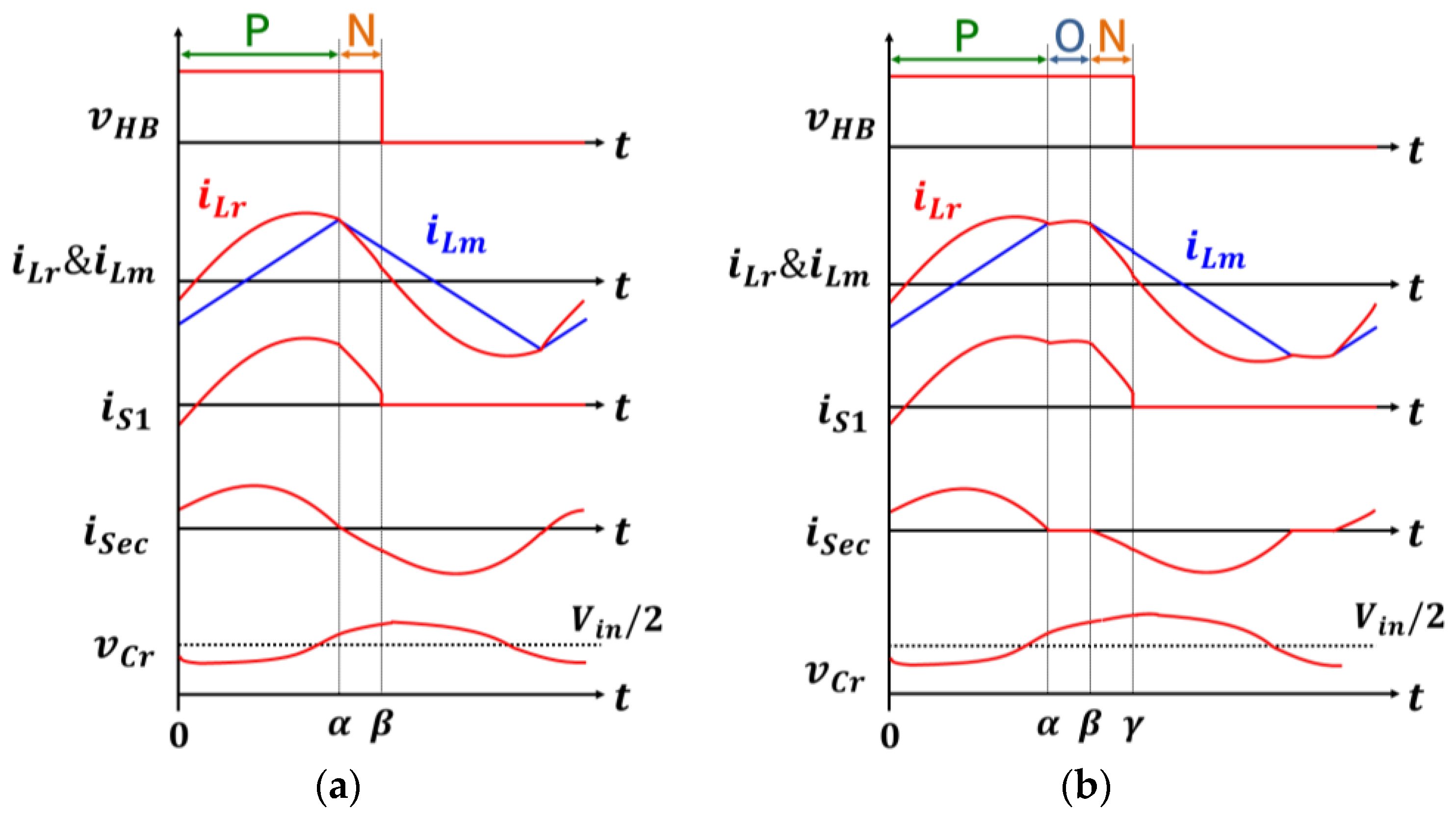
2.2. Classification of LLC Resonant Converter Operation Modes
The main operation modes of the LLC resonant converter can be classified as PO, PON, PN, P, O, NP, NOP, OP, and OPO. In addition to these nine operating modes, there are other possible combinations of P, N, and O subintervals; however, the corresponding operation mode exists in the zero current switching (ZCS) region, where the advantages of the MOSFET LLC resonant converter can be lost, so a detailed analysis is not performed. Consequently, the main operation region of the LLC resonant converter analyzed in this study is classified into three regions based on the resonant frequency, as follows: (1) the operation region where the operating frequency of the converter is less than the series resonant frequency ( < ), (2) the region where the operating frequency of the converter is equal to the series resonant frequency ( = ), and (3) the region where the operating frequency of the converter is greater than the series resonant frequency (> ) [10].
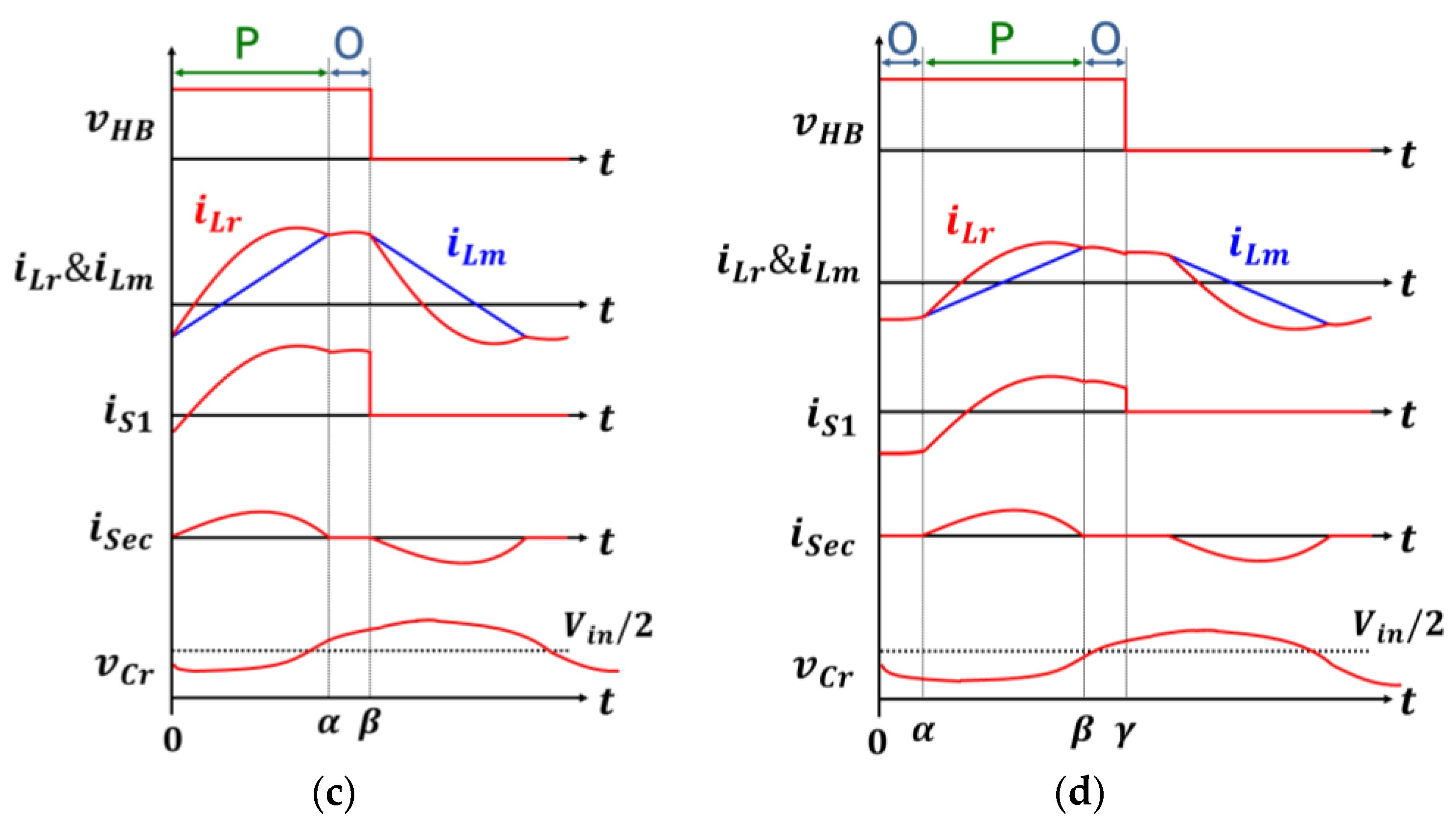
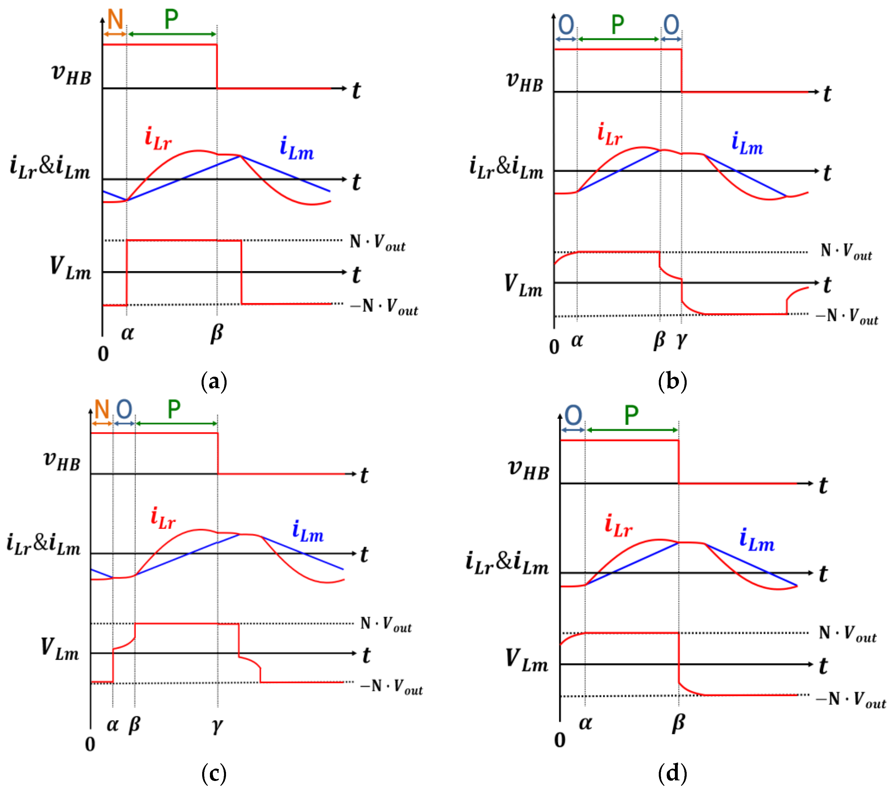
2.3. LLC Resonant Converter Operation Mode below Resonance
Figure 4 shows the waveforms of the representative operating modes of the LLC resonant converter in the < region. The PN and PON operation modes only appear in the ZVS and ZCS boundary conditions. In these modes, ZVS is partially guaranteed. In the PO operation mode, the switch current operates as a negative current when the switch is turned on, and consequently, the output cap of the switch is discharged to ensure ZVS operation. In the OPO operation mode, ZVS operation is guaranteed in the PO operation mode; however, this operation mode appears under a light load condition with a low load condition. The corresponding operation mode has an advantage in securing the stability of the control because of the increase in the input/output voltage gain with a decrease in the operating frequency. Thus, the design parameters must be adjusted so that it can operate in the corresponding region when designing an LLC resonant converter. Turn-on loss can be minimized by operating in the PO and OPO operation modes, and this can help achieve high efficiency. In addition, if the operating frequency is lowered continuously in the corresponding operation mode, the maximum voltage gain of the designed converter can be derived. The maximum voltage gain point determines the feasibility of the design when designing an LLC resonant converter.

Figure 4.
Representative operating mode waveforms in the LLC resonant converter fs < fr: (a) PN, (b) PON, (c) PO, and (d) OPO operation modes.
2.4. LLC Resonant Converter Operation Mode at Resonance
Figure 5 shows the P-operation mode of the LLC resonant converter at resonance. The voltage gain in the P-operation mode is calculated as unity regardless of the load size. In addition, there is no subinterval in which the energy circulates on the primary side. Further, a separate reverse recovery loss does not occur because the ZCS operation of the secondary-side rectifier diode can be guaranteed. These characteristics make it possible to achieve higher efficiency in the P-operation mode compared to that in the other operation modes.
Figure 5.
Representative operation mode waveform in the LLC resonant converter: P operation mode.
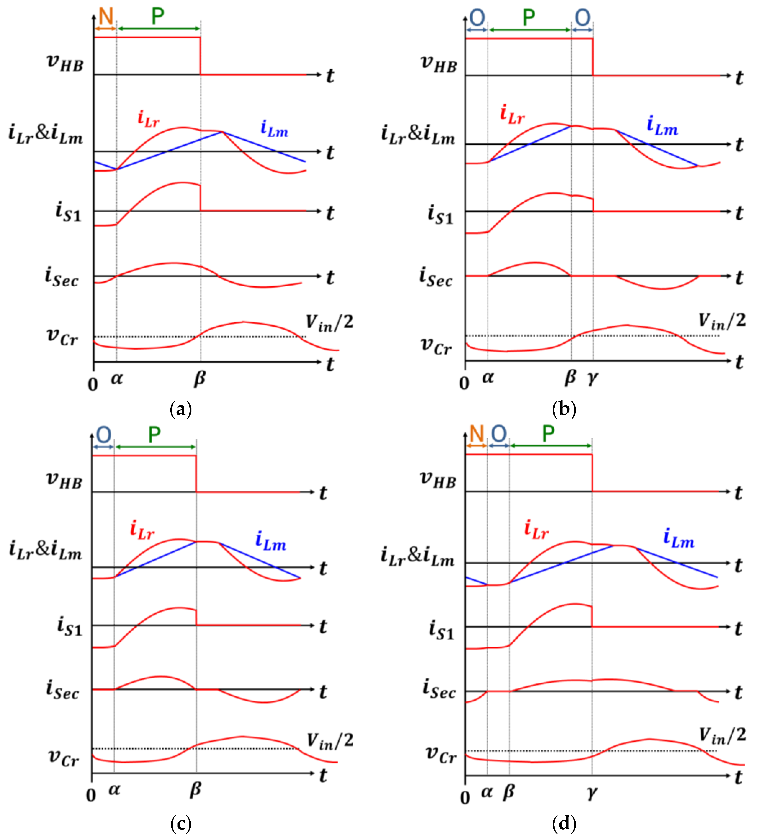
2.5. LLC Resonant Converter Operation Mode above Resonance
Figure 6 shows the voltage and current waveforms of the representative operation modes of the LLC resonant converter in the > region. Typically, there are four operation modes (NP, OPO, OP, and NOP), and the voltage gain of the resonant network is always lower than the unity gain in the corresponding region. The input impedance of the resonant network has an inductive load, and it guarantees the ZVS operation of the primary-side switch. However, the turn-off loss of the primary-side switch and the reverse recovery loss of the secondary-side rectifier diode increase during the switching operation. Therefore, avoiding this operation region is helpful when reducing power loss and achieving high efficiency.
Figure 6.
Representative operation mode waveforms in the LLC resonant converter (fs > fr): (a) NP, (b) OPO, (c) OP, and (d) NOP operation modes.
3. LLC Resonant Converter Analysis Algorithm
An algorithm that determines the operation mode and derives the voltage gain curve according to the operating conditions of the LLC resonant converter is proposed in this section based on the TDA-based LLC resonant converter analysis method. This algorithm helps to improve the design accuracy of the LLC resonant converter and achieve high efficiency and density at the design step.
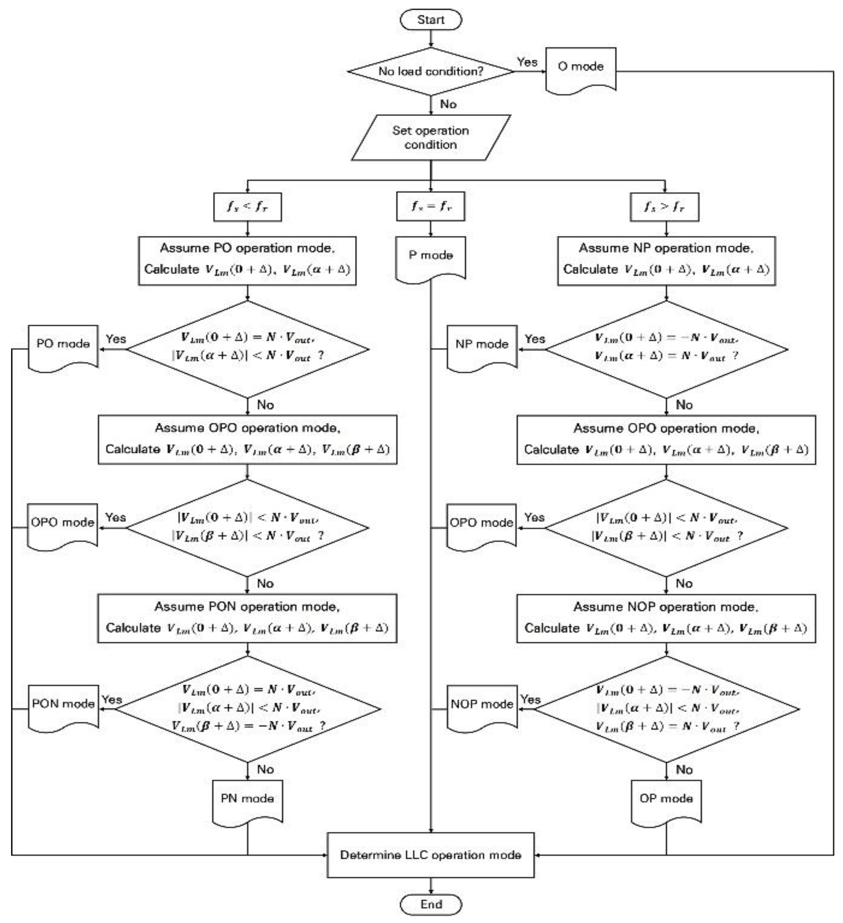
3.1. Operation Mode Determination Algorithm Considering Boundary Conditions
Analyzing the operating modes of a TDA-based LLC resonant converter is difficult because one equation cannot be applied to all operation modes. Thus, clarifying the equation for the operating state corresponding to each time interval and distinguishing the boundary conditions between the operating modes are necessary steps for analyzing the operating mode of the LLC resonant converter accurately.
The operation mode can be determined through a conditional expression for the magnitude of voltage across the magnetizing inductor according to the operating state of the converter [10]. Figure 7 shows the LLC resonant converter operation mode-classification algorithm. In the first step, it is determined whether there is a load or not; in the case of no load, it is determined as an O operation mode. Next, the magnitudes of the switching frequency and resonant frequency are compared and classified into three regions ( < , = , > ), and a conditional expression suitable for each operating frequency is employed. The = region is not classified through a separate conditional expression, and only the P operation mode exists.
Figure 7.
LLC resonant converter operation mode classification algorithm.
3.2. (Below Resonant Frequency Operation)
If < , the LLC resonant converter operation mode is assumed to be PO. Furthermore, the sizes of (0 + ∆) and are calculated, where α represents the length of the P subinterval and ∆ is an arbitrary value. The voltage waveform across the magnetizing inductor in the PO operation mode is shown in Figure 8a. If the conditional expression (0 + ∆) = or || < is satisfied, the corresponding operation mode is determined as the PO operation mode. If the PO operation mode determination condition is not satisfied, the OPO operation mode is assumed and the values of (0 + ∆) and (β + ∆) are calculated. The voltage waveform across the magnetizing inductor in the OPO operation mode is shown in Figure 8b. The OPO operation mode can be determined if the conditional expressions |(0 + ∆)| < and |(β + ∆)| < are satisfied. Similarly, if the determination condition of the OPO operation mode is not satisfied, the values of (0 + ∆), (α + ∆), and (β + ∆) are calculated by assuming the PON operation mode. The voltage waveform across the magnetizing inductor in the PON operation mode is shown in Figure 8c. The conditional expression (0 + ∆) = , |(α + ∆)| < , (β + ∆) = − is satisfied simultaneously, and it is determined as the PON operation mode. If none of the conditional expressions presented above are satisfied, the corresponding operation mode is determined as the PN operation mode. Figure 8d shows the voltage waveform across the magnetizing inductor in the PN operation mode.
Figure 8.
LLC resonant converter < operation mode waveform: (a) PO, (b) OPO, (c) PON, and (d) PN operation modes.
3.3. (Above Resonant Frequency Operation)
If > , then the LLC resonant converter operation mode is assumed to be the NP operation mode, and the magnitudes of (0 + ∆) and (α + ∆) are calculated. The voltage waveform across the magnetizing inductor in the NP operation mode is shown in Figure 9a. If the conditional expressions (0 + ∆) = − and (α + ∆) = are satisfied, it is determined as the NP operation mode. If the determination condition of the NP operation mode is not satisfied, the values of (0 + ∆) and (β + ∆) are calculated by assuming the OPO operation mode. The voltage waveform across the magnetizing inductor in the OPO operation mode is shown in Figure 9b. The OPO operation mode can be determined if the conditional expressions | (0 + ∆)| < and |(β + ∆)| < are satisfied. If the determination condition of the OPO operation mode is not satisfied, the magnitudes of (0 + ∆), (α + ∆), and (β + ∆) are calculated assuming the NOP operation mode. The voltage VLm waveform across the magnetizing inductor in the NOP operation mode is shown in Figure 9c. The conditional expression (0 + ∆) = −, |(α + ∆)| < , (β + ∆) = is satisfied simultaneously, and the NOP operation mode is determined. If none of the conditional expressions presented above are satisfied, the OP operation mode is determined. Figure 9d shows the voltage waveform across the magnetizing inductor in the OP operation mode.
Figure 9.
LLC resonant converter > operation mode waveform: (a) NP, (b) OPO, (c) NOP, and (d) OP operation modes.
4. Operating Mode Boundary Search and Voltage Gain Curve Derivation Algorithm
Figure 10 shows the TDA-based boundary search and voltage gain curve derivation algorithm for the LLC resonant converter. The operation mode can be classified based on the magnitude of the operation switching frequency and load using the proposed operation mode determination algorithm. The voltage gain value can be derived using the solver of the determined operation mode, and the voltage gain curve can be derived based on this analysis. For the TDA-based voltage gain curve, an appropriate formula must be applied according to the operating mode. A significant error can occur if the voltage gain is calculated without considering a specific operating mode. Thus, it is possible to derive a voltage gain curve that is considerably more similar to the actual result than the existing voltage gain curve based on the FHA.
Figure 10.
LLC resonant converter operation mode boundary classification and voltage gain curve derivation algorithm.
First, the algorithm proceeds by entering the design conditions (input voltage, resonance parameter, and number of turns). Second, the designer selects and inputs the minimum switching frequency , maximum switching frequency , and operation switching frequency interval required when executing the algorithm. The algorithm is executed by sequentially applying the load factor size interval . The algorithm is repeatedly performed within the range of the switching operating frequency and load factor. The execution is terminated when each variable reaches the maximum value. Finally, the derived information is stored temporarily until the next execution.
5. Performance Verification
The TDA-based resonant current and voltage gain values are compared with the values obtained from the experiment of the LLC resonant converter prototype. As shown in Figure 11, a 500 W LLC resonant converter experimental set is constructed and tested to validate the proposed algorithm. The primary side of the LLC resonant converter prototype has a half-bridge structure, and the switch to use is TP65H035GWS, which is manufactured by the Transphorm; the secondary side is a full-wave rectifier circuit structure, and the rectifier diode element is SCS320AE2HR. In addition, the resonant network is composed of a resonant inductor , resonant capacitor , and transformer with magnetizing inductance . A transformer with a turn ratio of 1.5 was manufactured for the conversion of the input and output voltage of the LLC converter, and the core used was EE6565, and the material type was FM10. In the case of winding, the number of turns on the primary side was six (turns), and the number of turns on the secondary side was four (turns) according to the values calculated using the transformer design procedure [11]. In addition, the transformer winding was manufactured using 9.3 (sq) and 13.6 (sq) Litz wires, and the diameter was 0.12 (mm). An MSO56 5-BW-500 oscilloscope from Tektronix, Beaverton, OR, U.S. was used for the measurement. The equipment used to measure the operating waveform, specifically in the case of Vgs voltage, was Tektronix’s THDP0200 Differential Probe, and the Vds voltage was measured using Tektronix’s TPP0500B Passive Probe. In addition, the resonance current was measured using a TCP0030A Current Probe. For the power supply and load simulation device, ITECH’s IT6018C-1500-40 was used. The TI TMS320F28337D controller was used to control the operating frequency of the LLC resonant converter. Table 1 lists the LLC resonant converter system parameters to verify the LLC resonant converter operation. The output voltage of the converter was controlled using the PFM (Pulse Frequency Modulation) method by adjusting the switching frequency within the range of 185–350 kHz. By adjusting the operating frequency, the desired output voltage could be obtained, and based on the input voltage of 210 (V), the minimum output voltage was 80 (V), the nominal output voltage was 100 (V), and the maximum output voltage was 120 (V). In order to find the total overall efficiency, it was necessary to calculate the loss, and the conduction loss of the transistors was calculated based on their on-resistance, and the switching loss included both turn-on and turn-off losses, as well as body diode reverse recovery losses. The turn-on loss was ignored assuming ZVS operation, and the turn-off loss, body diode reverse recovery loss, and the conduction loss of the diode in the secondary rectification stage were considered to calculate the overall efficiency. Depending on the load factor, the output efficiency was different, and it had an efficiency of 93.7% under the 50% load condition and 94.9 (%) efficiency under the 100% load condition.
Figure 11.
LLC resonant converter prototype experimental set configuration.
Table 1.
System parameters.
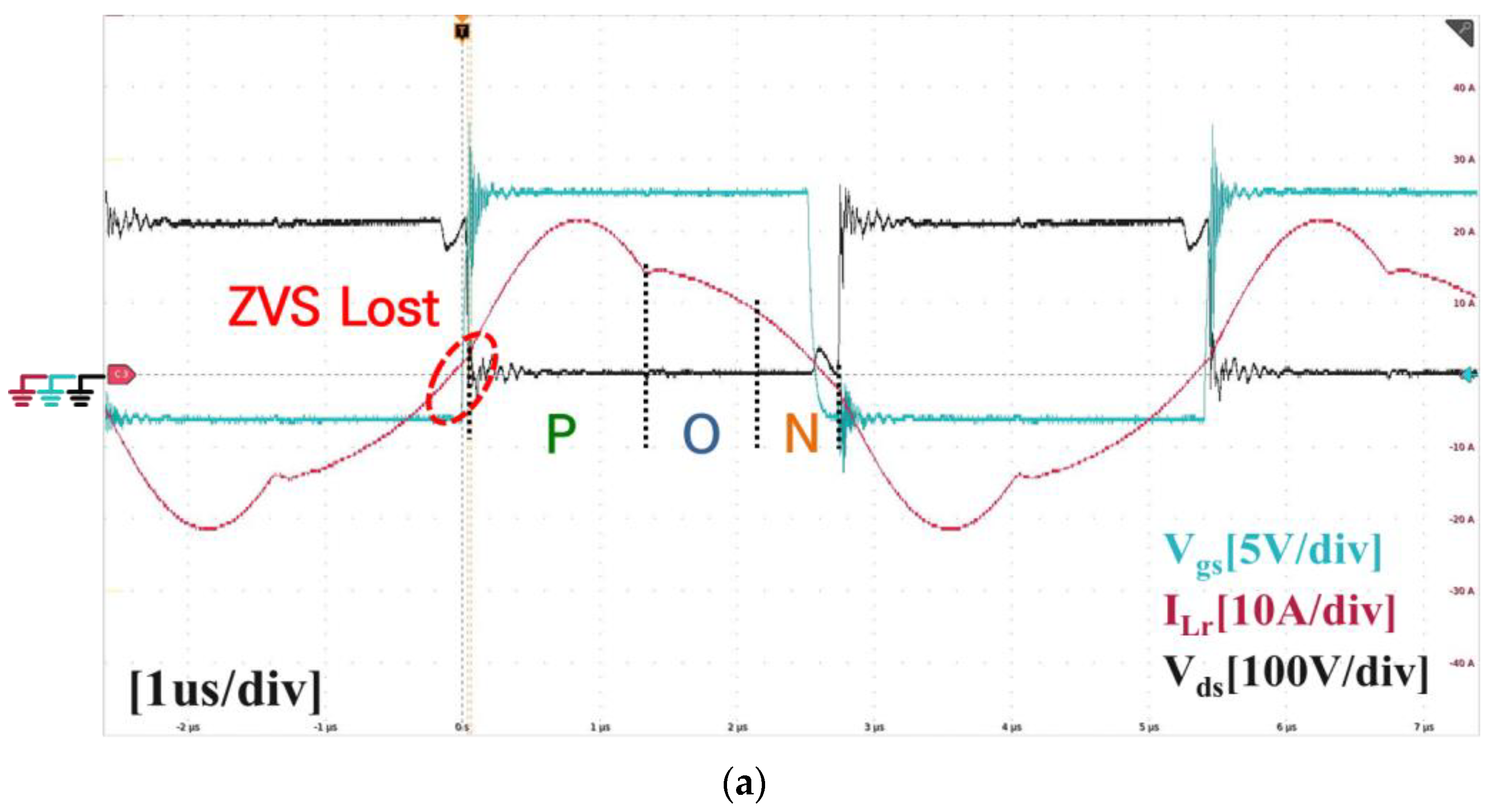
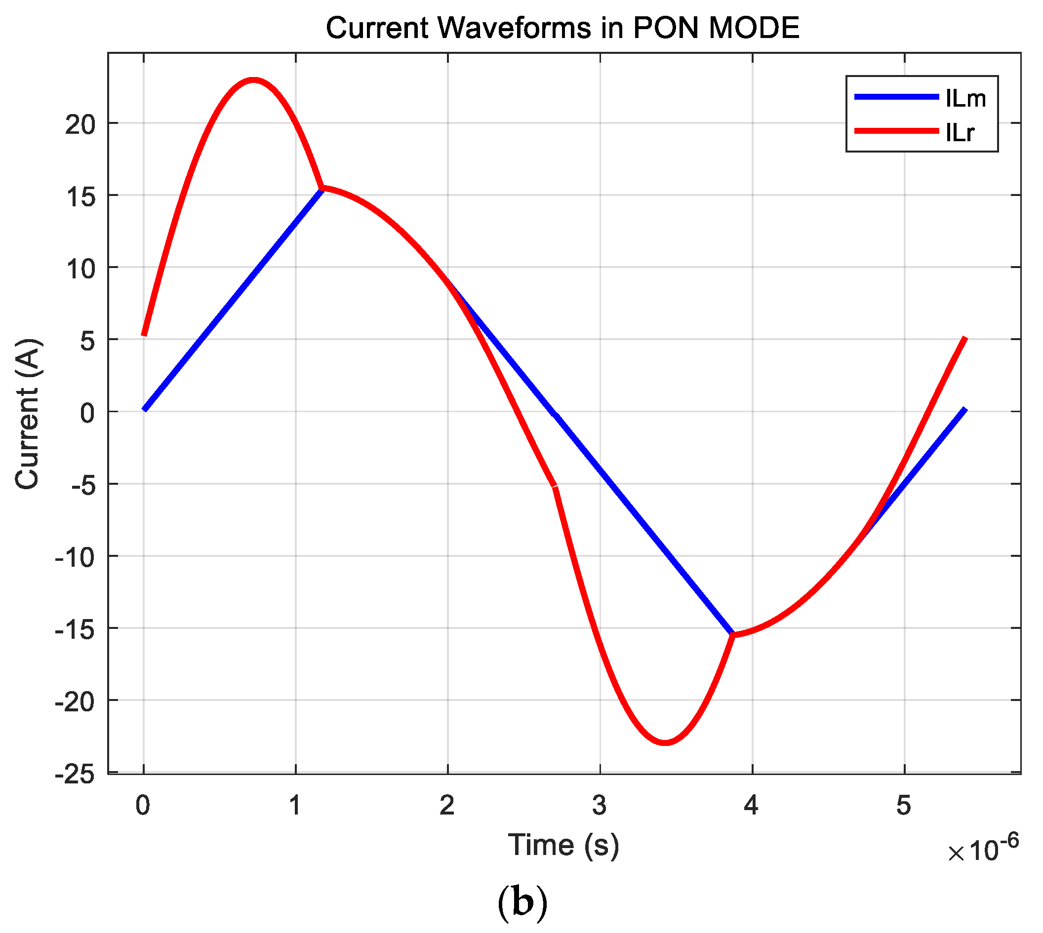
5.1. Comparison of the TDA Technique and Experimental Current Waveform
Figure 12a shows the gate-source and drain-source voltages and the resonant current waveforms of the primary-side switch of the LLC resonant converter prototype under the condition that the switching frequency is equal to the resonance frequency ( = 300 kHz). When the LLC resonant converter prototype operates in the P-mode, the resonant current appears as a sine waveform, and the ZVS operation of the primary-side switch can be achieved. Under the condition that operating frequency is 300 kHz, Figure 12b shows the resonant and magnetizing current waveforms of the P operation mode derived from the proposed TDA-based classification algorithm. Figure 13a shows the experimental waveform when the LLC resonant converter prototype operates at a switching frequency of 185 kHz. The prototype operates in the PON operation mode. If the switching frequency is reduced further at that point, the LLC resonant converter operates as a capacitive load and cannot achieve ZVS operation, as shown in the experimental waveform of the prototype in Figure 13a, which results in ringing on the source voltage. Therefore, the power loss may increase, and it may be difficult to secure control stability. Figure 13b shows the resonance and magnetizing current waveforms in the PON operation mode derived using the TDA-based classification algorithm. Results similar to the actual experimental waveform can be obtained. Figure 14a shows the experimental waveform when the LLC resonant converter prototype operated at a switching frequency of 330 kHz in the NP operation mode. When the switching frequency was higher than the resonance frequency, the voltage gain decreased with an increase in the switching frequency, and it achieved a ZVS operation similar to that in the PO operation mode. However, there was a possibility that the power loss may have increased because of the reverse recovery loss of the additional secondary-side rectifier diode. Figure 14b shows the resonant and magnetizing current waveforms in the NP operating mode, which were derived using the proposed TDA-based classification algorithm. As shown in Figure 14, the results are similar to the actual experimental waveform. Table 2 lists the results of the initial value, maximum value, and root mean square (RMS) of the resonance current value. The values derived from the TDA and the experiment are analyzed and compared. The error value in Table 2 represents the error of the result value obtained through actual experiment compared to the current value (initial value, peak value, and rms value) estimated using the TDA analysis technique, and the method of derivation is as follows:
Figure 12.
Waveform of LLC resonant converter at from experiment and TDA method: (a) prototype experiment, (b) TDA method.

Figure 13.
Waveform of LLC resonant converter at from experiment and TDA method: (a) prototype experiment, (b) TDA method.
Figure 14.
Waveform of LLC resonant converter at from experiment and TDA method: (a) prototype experiment, (b) TDA method.
Table 2.
Values extracted using the TDA method and the experiment.
5.2. Derivation of LLC Operation Boundary Curve and Comparison of LLC Resonant Converter Voltage Gain Curve
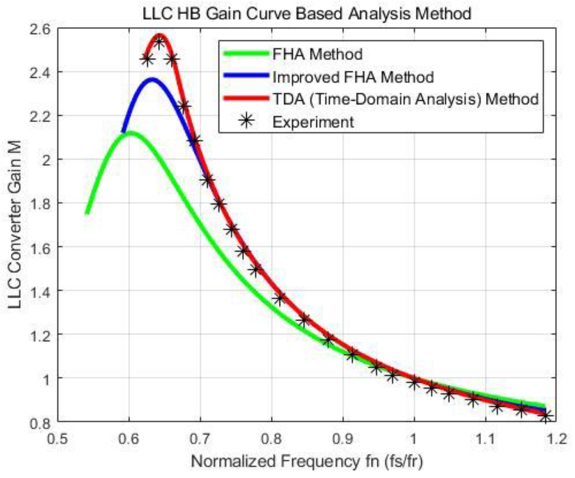
Figure 15a shows the LLC operation mode region based on the operating frequency and magnitude of the load obtained using the TDA-based boundary-mode classification algorithm. As shown in Figure 15a, the magnitude of the load and the operating frequency are normalized by the resonant frequency. When the boundary of the operating mode for each load size and operating frequency is determined, the voltage gain for each operating frequency is obtained using the proposed voltage gain curve derivation algorithm, as illustrated in Figure 15b. Figure 16 shows the results of the voltage gain values through experiments using the FHA, improved FHA, and TDA methods under the full-load 500 W LLC resonant converter. If the FHA and improved FHA methods are applied, the voltage gain curve can be derived using the equation of voltage gain, which is derived from the equivalent circuit that approximates the LLC resonant converter. However, the switching frequency exhibits a large error when it moves away from the resonant frequency. However, the voltage gain curve derived using the proposed TDA method shows high accuracy compared to that of the actual gain curve, which is derived from the LLC resonant converter prototype over the entire switching frequency range. Figure 17 shows the error of the voltage gain curve derived from the actual experiment and the voltage gain curve estimated by using each analysis method (FHA method, improved FHA method, and TDA method). In Figure 17, the voltage gain value at each operating frequency was calculated based on the measurement points for each operating frequency (23 points were selected in the experiment) in order to estimate the voltage gain curve in the actual experiment. The method to derive the gain curve estimation error is to calculate the average of the sum of the difference between the voltage gain value actually measured at each point and the voltage gain value estimated using the analysis method, and it can be expressed in the form of Equation (21).
k = number of measurement points in the experiment;
method = FHA, improved FHA, or TDA;
Exp = experiment.
Figure 15.
Operation mode distribution and voltage gain curve derived from the proposed algorithm: (a) operation mode boundary curve, (b) LLC HB gain curve.
Figure 16.
Voltage gain curve derived using various analysis techniques.
Figure 17.
Comparison of average error rate between the different analysis methods for the accurate gain curve.
The error was 8.4% on average in the case of the FHA method and 4.8% in the case of the improved FHA method. It was confirmed that the error rate of the TDA technique was only 0.7%. These results indicate that the gain curve can be estimated accurately when the TDA method is applied. Consequently, it can lead to the high-efficiency design of the LLC converter because it can precisely estimate not only the value of the current and voltage but also the voltage gain curve of the LLC resonant converter.
6. Conclusions
A method for accurately analyzing LLC resonant converters to increase their design accuracy was proposed in this paper. An algorithm for determining the LLC resonant converter operation mode and deriving the voltage gain curve was also proposed. According to the proposed TDA technique, the estimated error for the experimental results was around 2–4%. This allows for the accurate estimation of voltage and current magnitudes. Furthermore, when deriving the voltage gain curve of the LLC converter, the proposed TDA technique achieved higher accuracy compared to the existing FHA techniques. The estimated error of the proposed technique was 0.7%, which was significantly lower than the 7.7% estimated error of the commonly used FHA technique. Therefore, the proposed TDA technique can estimate the magnitude of current and voltage with high accuracy regardless of design conditions such as switching frequency and load size, which helps to improve the design accuracy of LLC resonant converters. This is advantageous for achieving high efficiency and high density. In addition, the proposed LLC resonant converter voltage gain curve derivation algorithm can be established to achieve high efficiency and density in the design stage. The accuracy of the TDA technique and effectiveness of the proposed algorithm were verified by comparing the experimental results of the 500 W LLC resonant converter prototype. However, as the TDA method is a kind of numerical-based analysis technique, it requires a significant number of computations. Furthermore, since the analysis is based on nonlinear relationships among design parameters, it may be somewhat difficult to intuitively understand the relationship between design parameters and results. Additionally, the scope of this research is limited to accurately estimating the voltage and current magnitudes, and it does not include analyses of losses or efficiency. Therefore, in order to design a high-efficiency resonant converter using this analysis, it is necessary to analyze loss and efficiency for each operation mode through the proposed method. Through this, it is possible to design a high-efficiency converter, and not only this, but research on the optimal design of a converter that can achieve both high efficiency and high density through accurate analysis techniques will also be conducted in the future.
Author Contributions
Conceptualization, S.-S.P. and M.-H.E.; methodology, S.-S.P. and M.-H.E.; software, S.-S.P. and M.-H.E.; validation, S.-S.P. and S.-T.L.; formal analysis, S.-S.P. and S.-T.L.; investigation, S.-S.P. and M.-H.E.; writing—original draft preparation, S.-S.P. and M.-H.E.; and writing—review and editing, S.-S.P. and R.-Y.K.; visualization, S.-S.P. and R.-Y.K.; supervision, R.-Y.K. All authors have read and agreed to the published version of the manuscript.
Funding
This work was supported by the Korea Institute of Energy Technology Evaluation and Planning (KETEP) grant funded by the Korean government (MOTIE) (No. 20202020800020).
Data Availability Statement
The dataset is not applicable.
Conflicts of Interest
The authors declare no conflict of interest.
References
- Gu, Z.; Tang, J.; Zhu, W.; Yao, K.; Gao, Z.; Shi, W.; Zhang, Z.; Ren, X. Comparison of wide-bandgap devices in 1 kV, 3 kW LLC converters. Chin. J. Elect. Eng. 2020, 6, 65–72. [Google Scholar] [CrossRef]
- Fang, X.; Hu, H.; Chen, F.; Somani, U.; Auadisian, E.; Shen, J.; Batarseh, I. Efficiency-oriented optimal design of the LLC resonant converter based on peak gain placement. IEEE Trans. Power Electron. 2012, 28, 2285–2296. [Google Scholar] [CrossRef]
- Choi, S.Y.; Kim, R.Y. Power Loss Analysis of Full-Bridge LLC Resonant Converter. In Proceedings of the 2021 24th International Conference on Electrical Machines and Systems (ICEMS), Gyeongju, Republic of Korea, 31 October–3 November 2021; IEEE: Manhattan, NY, USA, 2021; pp. 179–182. [Google Scholar]
- Yang, C.H.; Liang, T.J.; Chen, K.H.; Li, J.S.; Lee, J.S. Loss Analysis of Half-Bridge LLC Resonant Converter. In Proceedings of the 2013 1st International Future Energy Electronics Conference (IFEEC), Tainan, Taiwan, 3–6 November 2013; IEEE: Manhattan, NY, USA, 2013; pp. 155–160. [Google Scholar]
- Yang, B.; Lee, F.C.; Zhang, A.J.; Huang, G. LLC Resonant Converter for Front End DC/DC Conversion. In Proceedings of the Annual IEEE Conference on Applied Power Electronics Conference and Exposition (APEC), Dallas, TX, USA, 10–14 March 2002; Volume 2, pp. 1108–1112. [Google Scholar]
- Wei, Y.; Luo, Q.; Chen, S.; Sun, P.; Altin, N. Comparison among different analysis methodologies for LLC resonant converter. IET Power Electron. 2019, 12, 2236–2244. [Google Scholar] [CrossRef]
- Ivensky, G.; Bronshtein, S.; Abramovitz, A. Approximate analysis of resonant LLC DC-DC converter. IEEE Trans. Power Electron. 2011, 26, 3274–3284. [Google Scholar] [CrossRef]
- Liu, J.; Zhang, J.; Zheng, T.Q.; Yang, J. A modified gain model and the corresponding design method for an LLC resonant converter. IEEE Trans. Power Electron. 2016, 32, 6716–6727. [Google Scholar] [CrossRef]
- Glitz, E.S.; Ordonez, M. MOSFET Power Loss Estimation in LLC Resonant Converters: Time Interval Analysis. IEEE Trans. Power Electron. 2019, 34, 11964–11980. [Google Scholar] [CrossRef]
- Fang, X. Analysis and Design Optimization of Resonant DC-DC Converters. Ph.D. Thesis, University of Central Florida Orlando, Orlando, FL, USA, 2012. [Google Scholar]
- McLyman, W.T. Transformer and Inductor Design Handbook; Marcel Dekker: New York, NY, USA, 2004. [Google Scholar]
Disclaimer/Publisher’s Note: The statements, opinions and data contained in all publications are solely those of the individual author(s) and contributor(s) and not of MDPI and/or the editor(s). MDPI and/or the editor(s) disclaim responsibility for any injury to people or property resulting from any ideas, methods, instructions or products referred to in the content. |
© 2023 by the authors. Licensee MDPI, Basel, Switzerland. This article is an open access article distributed under the terms and conditions of the Creative Commons Attribution (CC BY) license (https://creativecommons.org/licenses/by/4.0/).