Abstract
This letter reports the phenomenon of current drops in an AlGaN/GaN heterojunction with CF4 plasma treated in a polar gas ambient. Ungated AlGaN/GaN HEMT with CF4 plasma treatment was tested in ethanol, acetonitrile, and an acetic acid gas ambient, and the current dropped by 52%, 51% and 61%, respectively, which are much higher than the drops (6%, 7%, and 8%) in normal ungated HEMT. On the one hand, based on “ambient doping”, a possible model was proposed to explain this phenomenon. On the other hand, the lower initial current was very important to increase the sensitivity. This means that the initial current should be elaborately designed to achieve maximum sensitivity.
1. Introduction
With the development of communications, computing, and other applications, integrated circuit systems continue to evolve toward being of a small size, having high power density, and having high operating frequency. AlGaN/GaN heterojunction high-electron-mobility transistor (HEMT) devices, with high mobility, high two-dimensional electron gas concentrations, wide band gaps, chemical stability, and other excellent characteristics, show greater application potential in high frequency, high power [1], ultraviolet (UV) photodetector [2] and sensor areas [3,4,5,6].
AlGaN/GaN HEMTs still have strong stability under extreme conditions such as high temperature, so more people use them as sensor devices [5,7,8,9]. Dropping polar liquid molecules on the surface of an AlGaN/GaN heterojunction will lead to channel current drops of up to 60%, which can be used for detecting polar liquids, such as ethanol, acetone, methanol, etc. [4,10], and for detecting inorganic liquids, such as HCl [11]. Due to the excellent characteristics of the AlGaN/GaN heterojunction’s structure, it can also be used as a gas sensor device. For example, a Pt/AlGaN/GaN HEMT structure was designed to detect H2, CO, NO, NO2, and NH3 [3,5,12], and in addition, a Pt/n-GaN structure, GaN Schottky, and metal-oxide-semiconductor (MOS) diode were also used for gas detection [13]. The theory is that the molecules were catalyzed into atoms at the surface of the Pt gate, and formed a dipolar layer, causing a reversible lowering of the Pt work function. However, the introduction of the expensive Pt metal makes the device’s process more complex. Is it possible to directly apply the AlGaN/GaN heterojunction for gas detection without Pt metal?
We observed a new phenomenon that in a polar organic gas ambient, the current of the AlGaN/GaN heterojunction with CF4 plasma treatment decreases, exhibiting higher sensitivity than the normal AlGaN/GaN heterojunction in both the dropping rate and the dropping amplitude. The current reduction is more than 50%. Based on the “ambient doping” [14] of the AlGaN/GaN heterojunction, we proposed a possible physical model, that is, the coupling of ambient dopants with surface polarization negative charges/fluorine negative charges to explain this phenomenon. This newly observed phenomenon probably provides a new approach for designing novel AlGaN/GaN heterojunction gas sensors that do not need Pt, which is expensive Pt. Incidentally, this phenomenon may also help people to understand the reason why the fluorine plasma-treated AlGaN/GaN heterojunction usually shows an unstable current in the air atmosphere.
2. Experiment
Two types of ungated HEMTs (A and B) were fabricated. Their structures are shown in Figure 1a,b. The epilayers were grown on a sapphire substrate via metalorganic chemical vapor deposition (MOCVD). From bottom to top, they consisted of a 6 µm thick unintentionally doped GaN buffer layer, 1 nm thick AlN interlayer, 21 nm thick Al0.26Ga0.74N barrier layer, and 2 nm thick GaN cap layer. The hall mobility was 1860 cm2/V s, and the 2DEG sheet density was 1.13 × 10¹³/cm2.
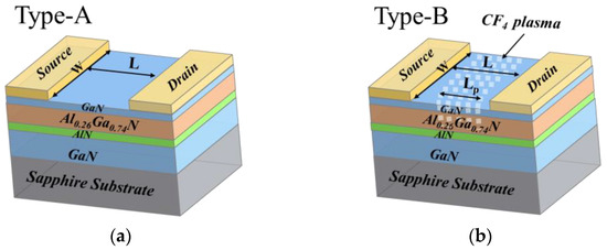
Figure 1.
Schematic diagram of the device structures. (a)Type-A ungated HEMTs without plasma treatment. (b) Type-B ungated HEMTs with CF4 plasma treatment.
The processes are as follows. Mesa isolation was performed using Cl2/BCl3 inductively coupled plasma (ICP). The Ohmic contacts were fabricated via e-beam evaporation of Ti/Al/Ni/Au (20/130/50/100 nm) stacks and then annealed at 870 °C for 30 s in a N2 atmosphere. After that, the B-type devices were treated by CF4 plasma to implant the F ions into the AlGaN barrier layer using APEX-ICP (inductively coupled plasma). The plasma treatment was performed with a RF power of 30 W, and ICP power of 600 W, and treating time was 2 min. The A-type devices were not treated by CF4 plasma. After the fabrication and dicing of the devices, the 5 × 5 mm2 chips were mounted on a printed circuit board (PCB). Wire bonding was carried out to connect the electrodes of the chips to the PCB electrodes.
There are two device geometries. L refers to the channel length. Lp refers to the length in the plasma treatment area. The L device is used for polar liquid testing, labeled as L, and the S device is used for polar gas testing, labeled as S. The L, Lp, and W of the L device are 1600 µm, 600 µm and 2200 µm, respectively. The L, Lp, and W of the S device are 100 µm, 60 µm and 400 µm, respectively. Hence, the ungated HEMTs are classified into four types, which are AL, AS, BL, and BS. The “L device” and “S device” have different dimensions, so we used the normalized current, Ids/(W/L), in Figure 2a. The I–V curves of the four samples are shown in Figure 2a. The linear region is located within the voltage range of −7~7 V.
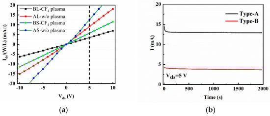
Figure 2.
(a) The I–V curves of AL, AS, BL, and BS. (b) Ids-t curves for type- A and -B device at Vds = 5 V.
A voltage of 5 V was applied on the samples with a sampling rate of 1 time per second. The Ids–t curves were recorded. In fact, there were trapping effects in our fabricated devices [15]. As shown in Figure 2b, at the beginning of the voltage bias, for type-A and type-B devices, the current is a bit high; over time, the current begins to drop, and after a while, the current stabilizes. For type-A devices without CF4 plasma treatment, the time for the current to reach stability is ~1000 s. CF4 plasma treatment increases the defect of the devices; therefore, trapping effects need to be excluded for a longer time, and the time for the current of type-B devices to reach stability is ~2000 s. In our experiments, the initial currents shown in the Ids–t curves are the stable currents. Thus, the trapping effects were excluded in the experiments.
In the following tests, Vds = 5 V was applied on the samples with a sampling rate of 1 time per second. After the current was stabilized, for the polar liquid testing, the polar liquids were dropped on the areas between the drain and source electrodes of AL and BL samples. For the polar gas test, the samples AS and BS were enclosed in a chamber, and the polar liquids were added along the side wall of the chamber, and they naturally volatilized to fill the chamber. The experimental results are shown in Figure 3. To observe the amount of current change, we normalized the current, as shown in Figure 3b,d.
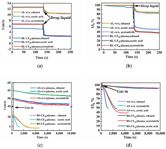
Figure 3.
(a) I–t curves affected by polar liquids. (b) Normalized I–t curves affected by polar liquids. (c) I–t curves affected by polar gases. (d) Normalized I–t curves affected by polar gases.
As shown in Figure 3a,b, the currents of the AL sample without F plasma treatment were reduced by about 1.9 mA (16%), 2.2 mA (17%) and 2.7 mA (19%) by ethanol, acetic acid and acetonitrile liquids, respectively. The currents of the BL sample with F plasma treatment were reduced by 2.6 mA (54%), 4.1 mA (61%) and 4.17 mA (63%) by ethanol, acetic acid and acetonitrile liquids, respectively. Comparing the currents of the AL and BL samples in the polar liquids, three differences could be observed. First of all, the current dropping rate of the BL is a little faster than that of AL. Secondly, the absolute current reductions in the BL sample are a little higher than those in the AL sample. Finally, the current reductions in the BL sample are much higher (>3.2 times) than those in the AL sample. These differences indicate that AlGaN/GaN heterojunctions with F plasma treatment are more sensitive to polar liquids than those without F plasma treatment are.
As shown in Figure 3c,d, the currents of the AS sample without F plasma treatment were reduced by about 3.25 mA (6%), 3.3 mA (7%), 3.5 mA (8%) by ethanol, acetic acid, acetonitrile gas ambient, respectively. The currents of the BL treatment with F plasma treatment were reduced by about 5.16 mA (52%), 4.71 mA (51%), 6.63 mA (61%) by ethanol, acetic acid, acetonitrile gas ambient, respectively. Compared with the AS and BS samples, the AL and BL samples show the same differences. However, the differences between the AS and BS samples are more significant. The current reduction rate of the BS sample (1000~2500 s) is more than 4 times that of the AS sample (~10,000 s). The current reductions in the BS sample (52%, 51%, and 61%) are more than 7 times those in the AS (6%, 7%, and 8%) sample. This means that AlGaN/GaN heterojunctions with CF4 plasma treatment are more sensitive to polar gases.
3. Discussion
Secondary ion mass spectrometry (SIMS) was used to characterize the distribution of the F element in the samples, as shown in Figure 4a.
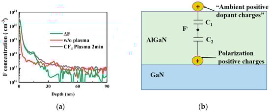
Figure 4.
(a) Distribution profiles of F elements within the treated and untreated samples; (b) Schematic diagram of the equivalent circuit to specify the positive charges compensating for F− ions.
Taking the F distribution of the sample without plasma treatment as the background, the F distribution of the sample with CF4 plasma treatment was calibrated, as shown in Figure 4. The red line is the F concentration of the device without plasma treatment, the black line is the F concentration of the device with CF4 plasma treatment, and the green line is the difference between those two devices. The F elements are almost located in the AlGaN barrier layer with a peak concentration close to the AlGaN surface. The total sheet density was calculated to be about 4.3 × 1013 cm−2, which is much higher than the 2DEG sheet density (~1 × 1013 cm−2). As reported by previous literature [16], F has deep energy levels (2.8 eV and 3.25 eV below the conduction band) in AlGaN/GaN heterojunctions. In AlGaN/GaN heterojunctions, the energy levels of most F elements are below Fermi level, and as a result, F elements should be negatively charged, i.e., by F− ions.
In the thermal equilibrium state of the AlGaN/GaN heterojunction, electric neutrality is a basic requirement. Those F− ions should be compensated by the same amount of positive charges coming from the AlGaN/GaN interface and AlGaN surface. Based on the static electricity principle, as shown in Figure 4b, the number of positive charges in an AlGaN/GaN interface and AlGaN surface could be estimated by the following equations.
where C1 and C2 are the equivalent capacitors from the location of F− in an AlGaN/GaN interface and AlGaN surface, respectively. QF is the number of F− ions in the AlGaN barrier. QP is the number of polarized positive charges at the AlGaN/GaN interface. QA is the number of positive charges at the AlGaN surface. As shown in Figure 4a, the F− ions gather nearby the AlGaN surface, in which case, C1 is larger than C2, resulting in QA > QP. QA and QP could be estimated to be ~3.5 × 1013 cm−2 and ~0.8 × 1013 cm−2. This explains why the 2DEG sheet density of ~1 × 1013 cm−2 not be fully depleted by the higher F− sheet density of ~4.3 × 1013 cm−2.
QP = −QF × C2/(C1 + C2)
QA = −QF × C1/(C1 + C2)
Although the origin of 2DEG in an AlGaN/GaN heterojunction is a controversial issue as yet, “ambient doping” sounds more reasonable, an states that “An important part of the origin of 2DEG in AlGaN/GaN heterojunction comes from the ambient doping [10,14,17]”. The high concentration of 2DEG in the AlGaN/GaN heterojunction obtained from environmental doping is associated with surface states and surface ions [14]. The occurrence of “ambient doping” implies that the QA in Equation (2) comes from the environmental positive ions (dopants) adsorbed on the AlGaN surface.
In an AlGaN/GaN heterojunction, as shown in Figure 5a, spontaneous and piezoelectric polarization induces positive and negative fixed charges at the interface and surface of the heterojunction [14,18]. Ambient doping causes positive ions to be adsorbed on the AlGaN surface, resulting in 2DEG generation in the channel. Two charge couplings have been established, i.e., polarization positive charges at the AlGaN/GaN interface with 2DEG in the channel, and the AlGaN surface’s polarized negative charges with the positive ions adsorbed on the AlGaN surface. For the fluorine plasma-treated AlGaN/GaN heterojunction, there were F− ions located in AlGaN barrier, as shown in Figure 5b. There were, additionally, two types of coupling dipoles. Some F− ions coupled with the positive polarization charges at the AlGaN/GaN interface, which reduced the 2DEG density. Other F− ions coupled with the positive surface ions. It should be noted that there were much more positive surface ions in the AlGaN/GaN heterojunction with fluorine plasma treatment than in the AlGaN/GaN heterojunction without fluorine plasma treatment.
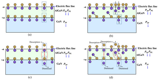
Figure 5.
Physical model diagrams of surface of AlGaN/GaN devices, (a) without plasma treatment, (b) with CF4 plasma treatment (c) without plasma treatment being affected by polar molecules, (d) and with CF4 plasma treatment being affected by polar molecules.
When polar liquids were dropped on the untreated AlGaN surface, those polar liquids dissolved the surface ions, namely producing a cleaning effect, as shown in Figure 5c. The original charge couplings were broken, and new charge couplings are established. The surface’s polarized negative charges coupled with the polarized positive charges. As a result of electric neutrality, the corresponding electrons in the channel disappeared, leading to the current drop.
For the fluorine plasma-treated AlGaN surface, as shown in Figure 5d, as long as the surface’s positive ions were dissolved by polar liquids, the couplings of surface negative polarization charges with surface positive ions are broken, and the couplings of F− charges with surface positive ions are broken too. As mentioned above, the dipole amount of the F− charges with surface positive ions was much more than that of surface negative polarization charges with surface positive ions. Furthermore, the dipole moment (that is determined by the distance between the negative charge and positive charge) of the F− charges with surface positive ions is larger than that of the surface’s negative polarization charges with surface positive ions. The surface positive ions of the fluorine-treated AlGaN/GaN heterojunction was more easily dissolved in a larger amount and at a faster rate than untreated one was. When surface positive ions were removed, the coupling of F− charges and surface positive ions was broken, and then the F− charges coupled with the polarized positive charges at the AlGaN/GaN interface. Due to electric neutrality, the number of electrons in the channel were also reduced by equal amounts.
In the vapor ambient, the dissolving capabilities of polar gases were reduced significantly, depending on the collision rate between the polar gas molecules and surface positive ions. The 2DEG reduction of the vapor case exhibited a slower rate and a smaller amount, compared with the polar liquid case. Due to the higher amount of surface positive charges (the collision rate was higher) and the larger dipole moment (desorption with lower energy) between surface positive ions and F− in the AlGaN barrier, the current of the fluorine plasma-treated AlGaN/GaN heterojunction shows a relatively faster dropping rate and a relatively larger reduction amount. For the fluorine plasma-treated AlGaN/GaN heterojunction, the initial current was much lower than that in the heterojunction without treatment. Hence, the relative current reductions were enlarged, as shown in Figure 3d, implying a lower initial current in fluorine plasma-treated AlGaN/GaN heterojunctions should exhibit higher sensitivity to polar gas vapors.
People have always found that the current of the fluorine plasma-treated AlGaN/GaN heterojunction is not very stable even in an air atmosphere [19,20]. This is possibly attributed to the existence of polar gases in the air atmosphere [10], which remove the “ambient dopants” from the surface [14].
4. Conclusions
In summary, we found that the AlGaN/GaN heterojunction with F plasma treatment was more sensitive to polar gas vapor than that without F plasma treatment. Based on “ambient doping”, we proposed a model to explain this phenomenon. In the AlGaN/GaN heterojunction with F plasma treatment, F− ions were incorporated in the AlGaN barrier, attracting more surface “ambient dopants” with a larger dipole moment, which could be easily removed by polar gas molecules. The initial current is an important factor affecting the current’s sensitivity. This phenomenon could reasonably explain the current instability of the AlGaN/GaN heterojunction with F plasma treatment in an air atmosphere. This phenomenon provides another possible approach to develop the AlGaN/GaN gas sensors without Pt, which is expensive, with a simpler fabrication process.
Author Contributions
Conceptualization, Y.C. and Y.M.; methodology Y.M. and Y.C.; investigation, Y.M., T.Z. and L.C.; writing—original draft, Y.M.; writing—review and editing, Y.C., Z.D., H.Q., L.M., B.Z. and Y.M.; supervision Y.C.; project administration, Y.H., Y.X. (Yang Xiao), Y.X. (Yijie Xin), Z.D., X.Z., G.Y. and Z.C. All authors have read and agreed to the published version of the manuscript.
Funding
This work was supported partly by the Key Research and Development Program of Jiangsu Province (no. BE2022057-1), the Key Research and Development Program of Jiangxi Province (no.20223BBE51033), the Youth Innovation Promotion Association of the Chinese Academy of Sciences (grant no. 2020321), and the National Natural Science Foundation of China (grant no. 92163204).
Data Availability Statement
The data that support the findings are available from the corresponding author upon reasonable request.
Acknowledgments
The authors would like to acknowledge Gebo Pan, Hongzhen Lin and Yi Cui for their fruitful discussions. Thanks go to Vacuum Interconnected Nanotech Workstation (Nano-X), Chinese Academy of Sciences (CAS), for supporting the test.
Conflicts of Interest
The authors declare no conflict of interest.
References
- Yong, C.; Yugang, Z.; Chen, K.J.; Lau, K.M. High-performance enhancement-mode AlGaN/GaN HEMTs using fluoride-based plasma treatment. IEEE Electron Device Lett. 2005, 26, 435–437. [Google Scholar] [CrossRef]
- Pandit, B.; Schubert, E.F.; Cho, J. Dual-functional ultraviolet photodetector with graphene electrodes on AlGaN/GaN heterostructure. Sci. Rep. 2020, 10, 22059. [Google Scholar] [CrossRef] [PubMed]
- Sokolovskij, R.; Zhang, J.; Zheng, H.; Li, W. The Impact of Gate Recess on the H2 Detection Properties of Pt-AlGaN/GaN HEMT Sensors. IEEE Sens. J. 2020, 20, 8947–8955. [Google Scholar] [CrossRef]
- Chaturvedi, N.; Singh, K.; Kachhawa, P.; Lossy, R. AlGaN/GaN HEMT based sensor and system for polar liquid detection. Sens. Actuators A Phys. 2020, 302, 111799. [Google Scholar] [CrossRef]
- Chung, G.H.; Vuong, T.A.; Kim, H. Demonstration of hydrogen sensing operation of AlGaN/GaN HEMT gas sensors in extreme environment. Results Phys. 2019, 12, 83–84. [Google Scholar] [CrossRef]
- Upadhyay, K.T.; Chattopadhyay, M.K. Sensor applications based on AlGaN/GaN heterostructures. Mater. Sci. Eng. B-Adv. Funct. Solid-State Mater. 2021, 263, 110312. [Google Scholar] [CrossRef]
- Raju, P.; Li, Q.L. Review-Semiconductor Materials and Devices for Gas Sensors. J. Electrochem. Soc. 2022, 169. [Google Scholar] [CrossRef]
- Sharma, N.; Kumar, S.; Gupta, A.; Bin Dolmanan, S. MoS2 functionalized AlGaN/GaN transistor based room temperature NO2 gas sensor. Sens. Actuators A-Phys. 2022, 342, 113647. [Google Scholar] [CrossRef]
- Kim, S.E.; Jang, S.Y.; Park, K.-H.; Lee, S.W. A route for an improved hydrogen sensing window using ZnO decorated Pt/AlGaN/GaN HEMT sensors. Ceram. Int. 2022, 48, 23590–23597. [Google Scholar] [CrossRef]
- Neuberger, R.; Muller, G.; Ambacher, O.; Stutzmann, M. High-electron-mobility AlGaN/GaN transistors (HEMTs) for fluid monitoring applications. Phys. Status Solidi A. 2001, 185, 85–89. [Google Scholar] [CrossRef]
- Mehandru, R.; Luo, B.; Kang, B.S.; Kim, J. AlGaN/GaN HEMT based liquid sensors. Solid-State Electron. 2004, 48, 351–353. [Google Scholar] [CrossRef]
- Bishop, C.; Halfaya, Y.; Soltani, A.; Sundaram, S. Experimental Study and Device Design of NO, NO2, and NH3 Gas Detection for a Wide Dynamic and Large Temperature Range Using Pt/AlGaN/GaN HEMT. IEEE Sens. J. 2016, 16, 6828–6838. [Google Scholar] [CrossRef]
- Kang, B.S.; Suku, K.; Ren, F.; Gila, B.P. AlGaN/GaN-based diodes and gateless HEMTs for gas and chemical sensing. IEEE Sens. J. 2005, 5, 677–680. [Google Scholar] [CrossRef]
- Ridley, B.K.; Ambacher, O.; Eastman, L.F. The polarization-induced electron gas in a heterostructure. Semicond. Sci Tech. 2000, 15, 270–271. [Google Scholar] [CrossRef]
- Angelotti, A.M.; Gibiino, G.P.; Florian, C.; Santarelli, A. Trapping Dynamics in GaN HEMTs for Millimeter-Wave Applications: Measurement-Based Characterization and Technology Comparison. Electronics 2021, 10, 137. [Google Scholar] [CrossRef]
- Kawakami, R.; Nakano, Y.; Niibe, M.; Shirahama, T. Electrical Investigation of Deep-Level Defects Introduced in AlGaN/GaN Heterostructures by CF4 Plasma Treatments. ECS Solid State Lett. 2015, 4, P36–P38. [Google Scholar] [CrossRef]
- Lingaparthi, R.; Dharmarasu, N.; Radhakrishnan, K.; Ranjan, A. Source of two-dimensional electron gas in unintentionally doped AlGaN/GaN multichannel high-electron-mobility transistor heterostructures. Appl. Phys. Lett. 2021, 118, 122105. [Google Scholar] [CrossRef]
- Ibbetson, J.P.; Fini, P.T.; Ness, K.D.; DenBaars, S.P. Polarization effects, surface states, and the source of electrons in AlGaN/GaN heterostructure field effect transistors. Appl. Phys. Lett. 2000, 77, 250–252. [Google Scholar] [CrossRef]
- Huang, S.; Chen, H.; Chen, K.J. In Surface properties of AlxGa1-xN/GaN heterostructures treated by fluorine plasma: An XPS study. In Proceedings of the International Workshop on Nitride Semiconductors (IWN)/Fall Meeting of the European-Materials-Research-Society (E-MRS)/Symposium N/Symposium H, Tampa, FL, USA, 19–24 September 2011. [Google Scholar]
- Wang, M.J.; Yuan, L.; Cheng, C.C. Defect formation and annealing behaviors of fluorine-implanted GaN layers revealed by positron annihilation spectroscopy. Appl. Phys. Lett. 2009, 94, 061910. [Google Scholar] [CrossRef]
Disclaimer/Publisher’s Note: The statements, opinions and data contained in all publications are solely those of the individual author(s) and contributor(s) and not of MDPI and/or the editor(s). MDPI and/or the editor(s) disclaim responsibility for any injury to people or property resulting from any ideas, methods, instructions or products referred to in the content. |
© 2023 by the authors. Licensee MDPI, Basel, Switzerland. This article is an open access article distributed under the terms and conditions of the Creative Commons Attribution (CC BY) license (https://creativecommons.org/licenses/by/4.0/).