


Numerical Investigation of Power Conversion Efficiency of Sustainable Perovskite Solar Cells
 , ,
, ,  ,
,  and
and 
Abstract
1. Introduction
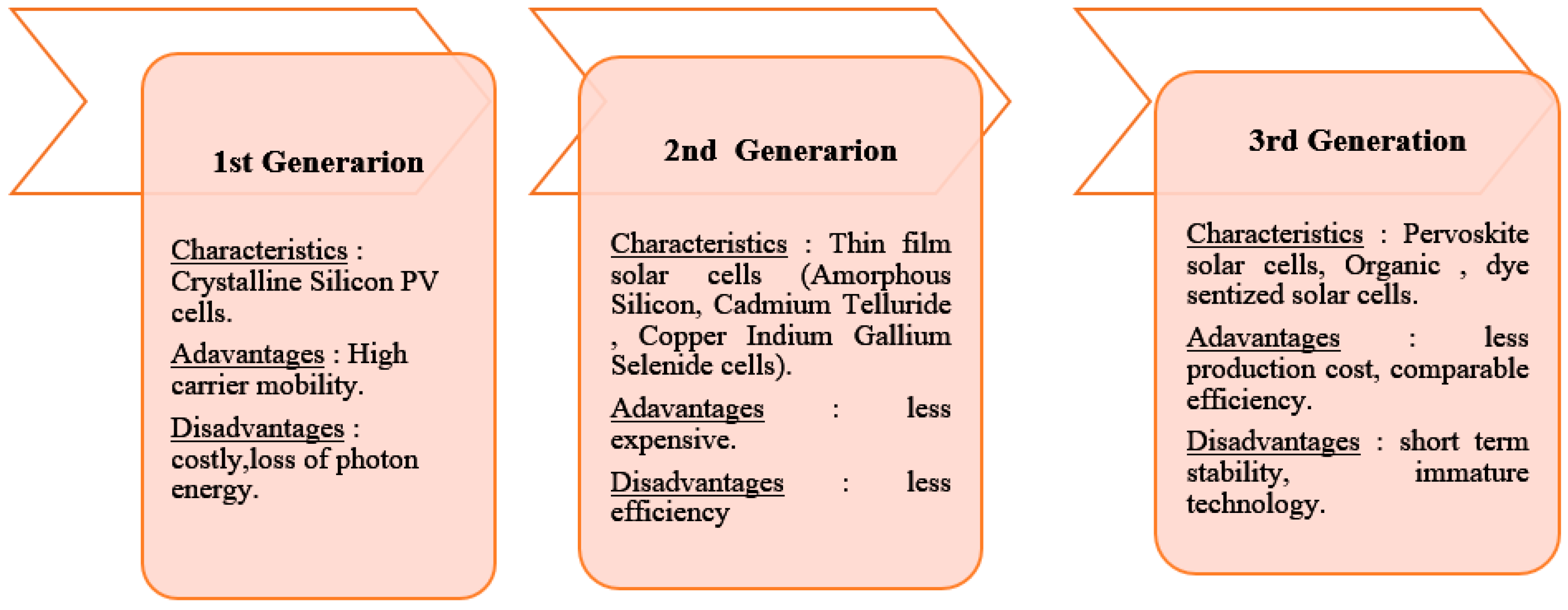
2. Background Works
3. Material and Methods
4. Results and Discussion
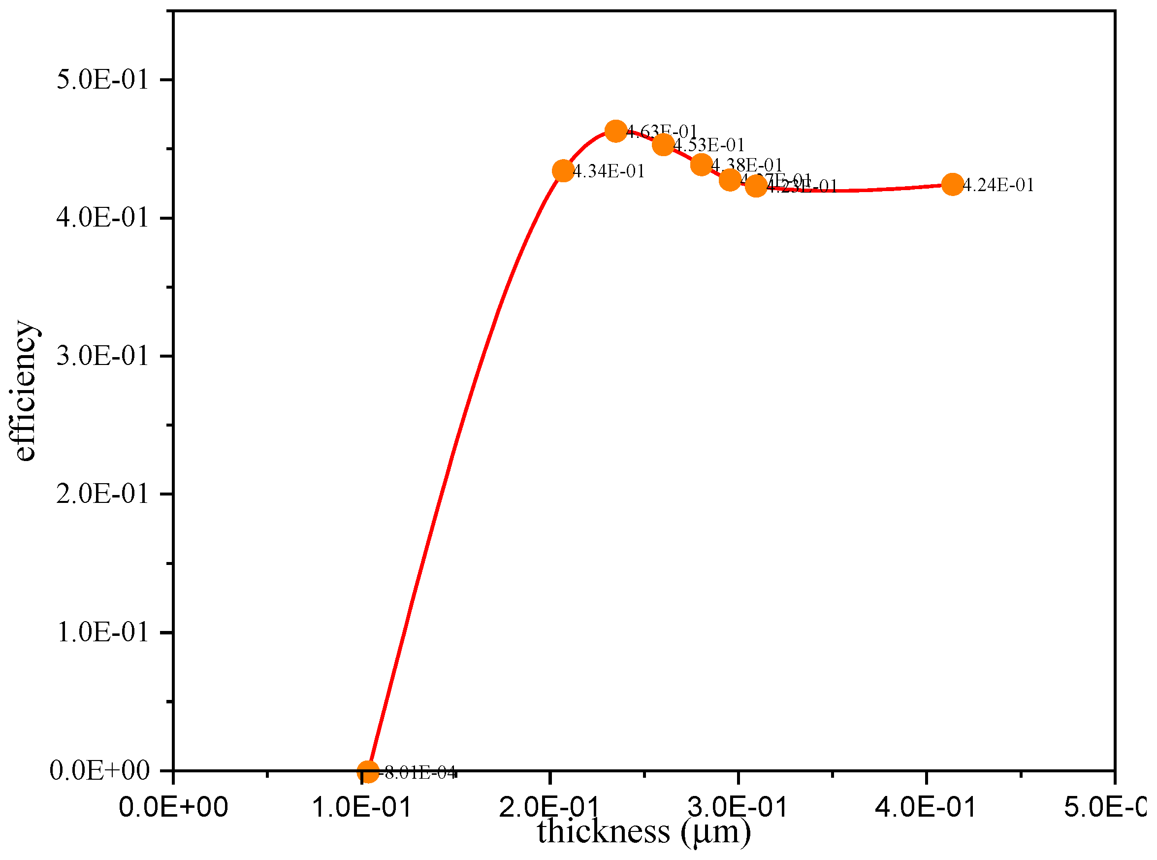
4.1. Effect of Thickness
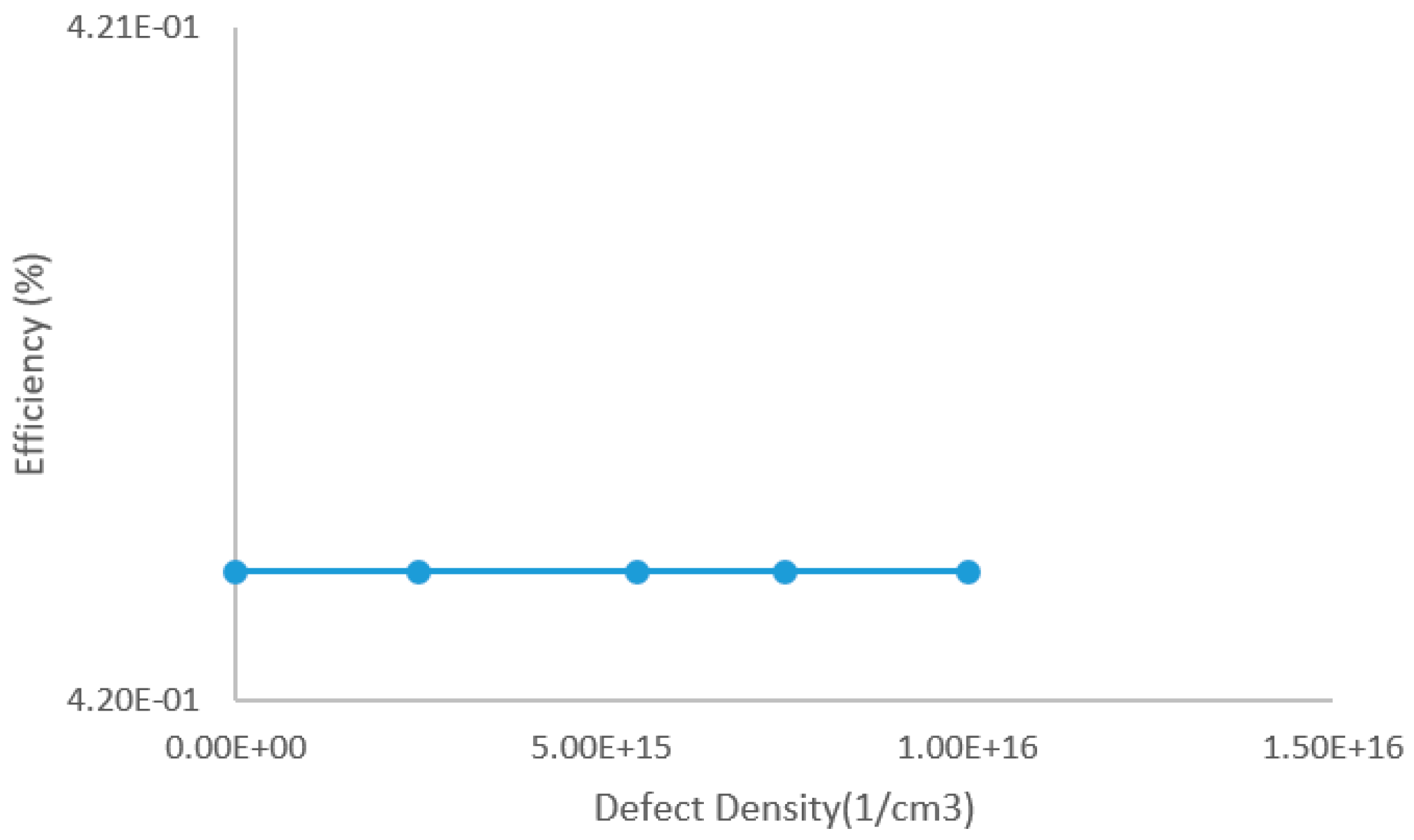
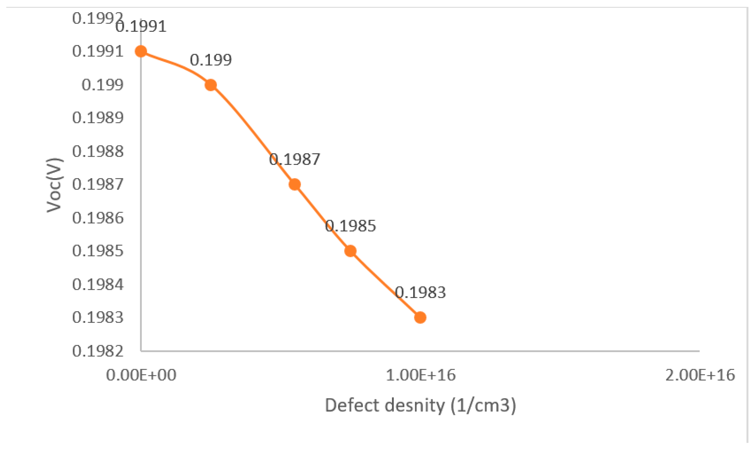
4.2. Effect of Defect Density
5. Conclusions
Author Contributions
Funding
Institutional Review Board Statement
Informed Consent Statement
Data Availability Statement
Acknowledgments
Conflicts of Interest
References
- Lee, M.M.; Teuscher, J.; Miyasaka, T.; Murakami, T.N.; Snaith, H.J. Efficient hybrid solar cells based on meso-superstructured organometal halide perovskites. Science 2012, 338, 643–647. [Google Scholar] [CrossRef]
- Jeong, J.; Kim, M.; Seo, J.; Lu, H.; Ahlawat, P.; Mishra, A.; Yang, Y.; Hope, M.A.; Eickemeyer, F.T.; Kim, M.; et al. Pseudo-halide anion engineering for α-FAPbI3 perovskite solar cells. Nature 2021, 592, 381–385. [Google Scholar] [CrossRef]
- Ishikawa, R.; Watanabe, S.; Yamazaki, S.; Oya, T.; Tsuboi, N. Perovskite/graphene solar cells without a hole-transport layer. ACS Appl. Energy Mater. 2019, 2, 171–175. [Google Scholar] [CrossRef]
- Tessler, N.; Vaynzof, Y. Preventing hysteresis in perovskite solar cells by undoped charge blocking layers. ACS Appl. Energy Mater. 2018, 1, 676–683. [Google Scholar] [CrossRef]
- Masood, M.T.; Weinberger, C.; Sarfraz, J.; Rosqvist, E.; Sandén, S.; Sandberg, O.J.; Vivo, P.; Hashmi, G.; Lund, P.D.; Osterbacka, R.; et al. Impact of film thickness of ultrathin dip-coated compact TiO2 layers on the performance of mesoscopic perovskite solar cells. ACS Appl. Materials Interfaces 2017, 9, 17906–17913. [Google Scholar] [CrossRef]
- Shalenov, E.O.; Dzhumagulova, K.N.; Seitkozhanov, Y.S.; Ng, A.; Valagiannopoulos, C.; Jumabekov, A.N. Insights on desired fabrication factors from modeling sandwich and quasi-interdigitated back-contact perovskite solar cells. ACS Appl. Energy Mater. 2021, 4, 1093–1107. [Google Scholar] [CrossRef]
- Wang, N.; Zhou, Y.; Ju, M.; Garces, H.F.; Ding, T.; Pang, S.; Zeng, X.C.; Padture, N.P.; Sun, X.W. Heterojunction-depleted lead-free perovskite solar cells with coarse-grained B-γ-CsSnI3 thin films. Adv. Energy Mater. 2016, 6, 1670137. [Google Scholar]
- Chung, I.; Song, J.H.; Im, J.; Androulakis, J.; Malliakas, C.D.; Li, H.; Freeman, A.J.; Kenney, J.T.; Kanatzidis, M.G. CsSnI3: Semiconductor or metal? High electrical conductivity and strong near-infrared photoluminescence from a single material. High hole mobility and phase-transitions. J. Am. Chem. Soc. 2012, 134, 8579–8587. [Google Scholar] [CrossRef]
- Minemoto, T.; Murata, M. Device modeling of perovskite solar cells based on structural similarity with thin film inorganic semiconductor solar cells. J. Appl. Phys. 2014, 116, 054505. [Google Scholar] [CrossRef]
- Ma, S.; Gu, X.; Kyaw, A.K.; Wang, D.H.; Priya, S.; Ye, T. Fully Inorganic CsSnI3-based solar cells with >6% efficiency and enhanced stability enabled by mixed electron transport layer. ACS Appl. Mater. Interfaces 2021, 13, 1345–1352. [Google Scholar] [CrossRef]
- Wang, Y.; Tu, J.; Li, T.; Tao, C.; Deng, X.; Li, Z. Convenient preparation of CsSnI3 quantum dots, excellent stability, and the highest performance of lead-free inorganic perovskite solar cells so far. J. Mater. Chem. A 2019, 7, 7683–7690. [Google Scholar] [CrossRef]
- Ye, T.; Wang, X.; Wang, K.; Ma, S.; Yang, D.; Hou, Y.; Yoon, J.; Wang, K.; Priya, S. Localized electron density engineering for stabilized B-γ CsSnI3-based perovskite solar cells with efficiencies >10%. ACS Energy Lett. 2021, 6, 1480–1489. [Google Scholar] [CrossRef]
- Adhikari, K.R.; Gurung, S.; Bhattarai, B.K.; Soucase, B.M. Comparative study on MAPbI3 based solar cells using different electron transporting materials. Phys. Status Solidi C 2016, 13, 13–17. [Google Scholar] [CrossRef]
- Etgar, L.; Gao, P.; Xue, Z.S.; Peng, Q.; Chandiran, A.K.; Liu, B.; Nazeeruddin, M.K.; Grätzel, M. Mesoscopic CH3NH3PbI3/TiO2 heterojunction solar cells. J. Am. Chem. Soc. 2012, 134, 17396–17399. [Google Scholar] [CrossRef]
- Laban, W.A.; Etgar, L. Depleted hole conductor-free lead halide iodide heterojunction solar cells. Energy Environ. Sci. 2013, 6, 3249–3253. [Google Scholar] [CrossRef]
- Aharon, S.; Gamliel, S.; El Cohen, B.; Etgar, L. Depletion region effect of highly efficient hole conductor free CH3NH3PbI3 perovskite solar cells. Phys. Chem. Chem. Phys. 2014, 16, 10512–10518. [Google Scholar] [CrossRef] [PubMed]
- Aharon, S.; El Cohen, B.; Etgar, L. Hybrid lead halide iodide and lead halide bromide in efficient hole conductor free perovskite solar cell. J. Phys. Chem. C 2014, 118, 17160–17165. [Google Scholar] [CrossRef]
- Xiao, L.X.; Zou, D.C. Perovskite Solar Cells, 2nd ed.; Peking University Press: Beijing, China, 2020. [Google Scholar]
- Chen, J.Y.; Chen, F.X.; Xu, W.K.; Cao, G.H.; Wang, L.S. Simulation optimization of planar heterojunction perovskite solar cells with B-γ-CsSnI3 as optical absorption layer. J. Synth. Cryst. 2018, 47, 31–36. [Google Scholar]
- Fonash, S.J. AMPS Manual. 2010. Available online:http://www.ampsmodeling.org/pdfs/AMPS-1D%20Manual.pdf (accessed on 10 November 2022).
- Lin, S.; Li, X.R.; Pan, H.Q.; Chen, H.T.; Li, X.Y.; Li, Y.; Zhou, J.R. Numerical analysis of InxGa1-xN/SnS and AlxGa1-xN/SnS heterojunction solar cells. Energy Convers. Manag. 2016, 119, 361–367. [Google Scholar] [CrossRef]
- Ghorbani, E. On efficiency of earth-abundant chalcogenide photovoltaic materials buffered with CdS: The limiting effect of band alignment. J. Phys. Energy 2020, 2, 025002. [Google Scholar] [CrossRef]
- Marshall, K.P.; Walton, R.I.; Hatton, R.A. Tin perovskite/fullerene planar layer photovoltaics: Improving the efficiency and stability of lead-free devices. J. Mater. Chem. A 2015, 3, 11631–11640. [Google Scholar] [CrossRef]
- Marshall, K.P.; Walker, M.; Walton, R.I.; Hatton, R.A. Enhanced stability and efficiency in hole-transport-layer-free CsSnI3 perovskite photovoltaics. Nat. Energy 2016, 1, 16178. [Google Scholar] [CrossRef]
- Wu, B.; Zhou, Y.; Xing, G.; Xu, Q.; Garces, H.F.; Solanki, A.; Goh, T.W.; Padture, N.P.; Sum, T.C. Long minority-carrier diffusion length and low surface-recombination velocity in inorganic lead-free CsSnI3 perovskite crystal for solar cells. Adv. Funct. Mater. 2017, 27, 1604818. [Google Scholar] [CrossRef]
- Bin, Z.; Li, J.; Wang, L.; Duan, L. Efficient n-type dopants with extremely low doping ratios for high performance inverted perovskite solar cells. Energy Environ. Sci. 2016, 9, 3424–3428. [Google Scholar] [CrossRef]
- Shao, S.; Abdu-Aguye, M.; Qiu, L.; Lai, L.H.; Liu, J.; Adjokatse, S.; Jahani, F.; Kamminga, M.E.; ten Brink, G.H.; Palstra, T.T.M.; et al. Elimination of the light soaking effect and performance enhancement in perovskite solar cells using a fullerene derivative. Energy Environ. Sci. 2016, 9, 2444–2452. [Google Scholar] [CrossRef]
- Konstantakou, M.; Stergiopoulos, T. A critical review on tin halide perovskite solar cells. J. Mater. Chem. A 2017, 5, 11518–11549. [Google Scholar] [CrossRef]
- Castro, E.; Fernandez-Delgado, O.; Arslan, F.; Zavala, G.; Yang, T.; Seetharaman, S.; D’Souza, F.; Echegoyen, L. New thiophene-based C60 fullerene derivatives as efficient electron transporting materials for perovskite solar cells. New J. Chem. 2018, 42, 14551–14558. [Google Scholar] [CrossRef]
- Shao, S.; Liu, J.; Fang, H.H.; Qiu, L.; ten Brink, G.H.; Hummelen, J.C.; Koster, L.J.A.; Loi, M.A. Efficient perovskite solar cells over a broad temperature window: The role of the charge carrier extraction. Adv. Energy Mater. 2017, 7, 1701305. [Google Scholar] [CrossRef]
- Golubev, T.; Liu, D.; Lunt, R.; Duxbury, P. Understanding the impact of C60 at the interface of perovskite solar cells via drift-diffusion modeling. AIP Adv. 2019, 9, 035026. [Google Scholar] [CrossRef]
- Zhao, P.; Liu, Z.; Lin, Z.; Chen, D.; Su, J.; Zhang, C.; Zhang, J.; Chang, J.; Hao, Y. Device simulation of inverted CH3NH3PbI3−xClx perovskite solar cells based on PCBM electron transport layer and NiO hole transport layer. Sol. Energy 2018, 169, 11–18. [Google Scholar] [CrossRef]
- Tai, Q.; Tang, K.-C.; Yan, F. Recent progress of inorganic perovskite solar cells. Energy Environ. Sci. 2019, 12, 2375–2405. [Google Scholar] [CrossRef]
- Gao, W.; Li, P.; Chen, J.; Ran, C.; Wu, Z. Interface engineering in tin perovskite solar cells. Adv. Mater. Interfaces 2019, 6, 1901322. [Google Scholar] [CrossRef]
- Liu, Z.; Krückemeier, L.; Krogmeier, B.; Klingebiel, B.; Márquez, J.A.; Levcenko, S.; Öz, S.; Mathur, S.; Rau, U.; Unold, T.; et al. Open-circuit voltages exceeding 1.26 V in planar methylammonium lead iodide perovskite solar cells. ACS Energy Lett. 2019, 4, 110–117. [Google Scholar] [CrossRef]
- Wang, H.-Q.; Xu, J.; Lin, X.; Li, Y.; Kang, J.; Zheng, J.-C. Determination of the embedded electronic states at nanoscale interface via surface-sensitive photoemission spectroscopy. Light: Sci. Appl. 2021, 10, 153. [Google Scholar] [CrossRef]
- Le Corre, V.M.; Stolterfoht, M.; Toro, L.P.; Feuerstein, M.; Wolff, C.; Gil-Escrig, L.; Bolink, H.J.; Neher, D.; Koster, L.J.A. Charge transport layers limiting the efficiency of perovskite solar cells: How to optimize conductivity. ACS Appl. Energy Mater. 2019, 2, 6280–6287. [Google Scholar] [CrossRef]
- Bhojak, V.; Bhatia, D.; Jain, P.K. Investigation of photocurrent efficiency of Cs2TiBr6 double perovskite solar cell. Mater. Today Proc. 2022, 66, 3692–3697. [Google Scholar] [CrossRef]
- Abhishek, R.; Avneesh, A.; Vinita, T. Effect of appropriate ETL on quantum efficiency of double perovskite LMNO based solar cell device via SCAPS simulation. Mater. Today Proc. 2021, 47, 1656–1659. [Google Scholar]
- Mariello, M. Recent Advances on Hybrid Piezo-Triboelectric Bio-Nanogenerators: Materials, Architectures and Circuitry. Nanoenergy Adv. 2022, 2, 64–109. [Google Scholar] [CrossRef]


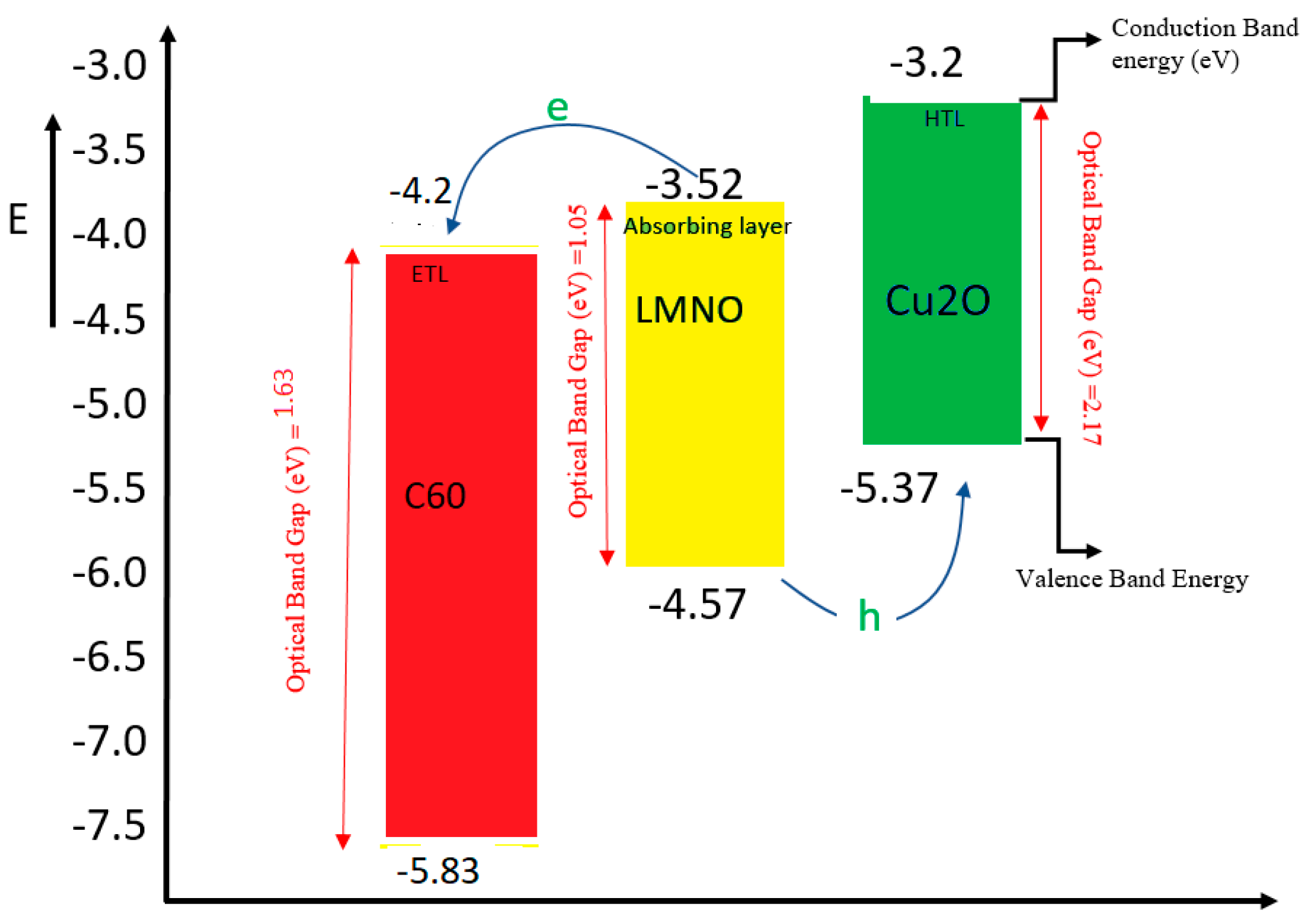
| Material Properties | TiO2 | LMNO | C60 | ZnO | Cu2O | FTO | CuI |
|---|---|---|---|---|---|---|---|
| Layer thickness (nm) | 30 | 350 | 30 | 30 | 200 | 500 | 200 |
| Optical bandgap(eV) | 3.2 | 1.05 | 1.7 | 3.3 | 2.17 | 3.5 | 3.1 |
| Affinity of electron (eV) | 3.9 | 3.52 | 3.9 | 4 | 3.2 | 4 | 2.1 |
| Relative permittivity | 32 | 3.5 | 4.2 | 9 | 7.11 | 9 | 6.5 |
| Effective DOS in the conduction band (cm−3) | 1 × 10¹⁹ | 1 × 10¹⁸ | 8 × 10¹⁹ | 2 × 10¹⁸ | 2.2 × 10¹⁸ | 2.2 × 10¹⁸ | 2.2 × 10¹⁸ |
| Effective DOS in the valance band (cm−3) | 1 × 10¹⁹ | 1 × 10¹⁸ | 8 × 10¹⁹ | 1.8 × 10¹⁹ | 1.9 × 10¹⁹ | 1.8 × 10¹⁹ | 1.8 × 10¹⁹ |
| Thermal velocity of electron (cm/s) | 107 | 107 | 107 | 107 | 107 | 107 | 107 |
| Thermal velocity of hole (cm/s) | 107 | 107 | 107 | 107 | 107 | 107 | 107 |
| Mobility of electron (cm2/Vs) | 20 | 22 | 1 × 10⁻² | 100 | 3 × 10² | 20 | 100 |
| Hole mobility (cm2/Vs) | 10 | 22 | 3.5 × 10⁻³ | 25 | 8 × 101 | 10 | 47.9 |
| Donor density (cm−3) | 1 × 10¹⁷ | - | 2.6 × 10¹⁸ | 1 × 10¹⁸ | - | 1 × 10¹⁹ | - |
| Acceptor density (cm−3) | - | 7 × 10¹⁶ | - | - | 1 × 10¹⁸ | - | 1 × 10¹⁸ |
| Defect density | 1014 | 1014 | 1014 | 1014 | 1014 | 1014 | 1014 |
| Structure | JSC | VOC | FF | Efficiency (%) |
|---|---|---|---|---|
| C60/LMNO/Cu2O | 3.71 | 0.202 | 56.83 | 0.43 |
| TiO2/LMNO/CuI | 1.92 | 0.1919 | 49.5 | 0.18 |
| C60/LMNO/CuI | 1.91 | 0.1838 | 48.44 | 0.17 |
| ZnO/LMNO/Cu2O | 0.003 | 0.1873 | 52.11 | 0.01 |
| Thickness | Efficiency | Voc(V) |
|---|---|---|
| 1.00 × 10⁻¹ | 4.20 × 10⁻¹ | 0.2009 |
| 1.00 × 100 | 4.30 × 10⁻¹ | 0.2018 |
| 1.50 × 100 | 4.30 × 10⁻¹ | 0.202 |
| 2.00 × 100 | 4.30 × 10⁻¹ | 0.2021 |
| Defect Density | Efficiency | Voc |
|---|---|---|
| 1.00 × 10¹⁰ | 4.20 × 10⁻¹ | 0.199 |
| 2.50 × 10¹⁵ | 4.20 × 10⁻¹ | 0.199 |
| 5.50 × 10¹⁵ | 4.20 × 10⁻¹ | 0.198 |
| 7.50 × 10¹⁵ | 4.20 × 10⁻¹ | 0.198 |
| 1.00 × 10¹⁶ | 4.20 × 10⁻¹ | 0.198 |
| Structure | VOC | JSC | FF | PCE | Parameters Optimized |
|---|---|---|---|---|---|
| C60/LMNO/Cu2O (Proposed) | 0.1919 | 1.92 | 49.5 | 0.43 | ETL, HTL, thickness of absorbing layer, defect density |
| C60/Perovskite/CuI [40] | 0.1982 | 1.9110 | 47.82 | 0.18 | ETL and work function |
Disclaimer/Publisher’s Note: The statements, opinions and data contained in all publications are solely those of the individual author(s) and contributor(s) and not of MDPI and/or the editor(s). MDPI and/or the editor(s) disclaim responsibility for any injury to people or property resulting from any ideas, methods, instructions or products referred to in the content. |
© 2023 by the authors. Licensee MDPI, Basel, Switzerland. This article is an open access article distributed under the terms and conditions of the Creative Commons Attribution (CC BY) license (https://creativecommons.org/licenses/by/4.0/).
Share and Cite
Bhojak, V.; Jain, P.K.; Bhatia, D.; Dargar, S.K.; Jasinski, M.; Gono, R.; Leonowicz, Z. Numerical Investigation of Power Conversion Efficiency of Sustainable Perovskite Solar Cells. Electronics 2023, 12, 1762. https://doi.org/10.3390/electronics12081762
Bhojak V, Jain PK, Bhatia D, Dargar SK, Jasinski M, Gono R, Leonowicz Z. Numerical Investigation of Power Conversion Efficiency of Sustainable Perovskite Solar Cells. Electronics. 2023; 12(8):1762. https://doi.org/10.3390/electronics12081762
Chicago/Turabian StyleBhojak, Vivek, Praveen K. Jain, Deepak Bhatia, Shashi Kant Dargar, Michał Jasinski, Radomir Gono, and Zbigniew Leonowicz. 2023. "Numerical Investigation of Power Conversion Efficiency of Sustainable Perovskite Solar Cells" Electronics 12, no. 8: 1762. https://doi.org/10.3390/electronics12081762
APA StyleBhojak, V., Jain, P. K., Bhatia, D., Dargar, S. K., Jasinski, M., Gono, R., & Leonowicz, Z. (2023). Numerical Investigation of Power Conversion Efficiency of Sustainable Perovskite Solar Cells. Electronics, 12(8), 1762. https://doi.org/10.3390/electronics12081762