Abstract
Vehicle electrification and digitalization are even more and more increasingly pushed by several aims, such as the improvement in sustainability, wellness, safety, and reliability. The need for onboard power electronics is a common factor for the different types of electric vehicles. Similarly, the increasing presence of onboard Internet of Things items as well as systems implementing artificial intelligence asks for additional power electronics that ensure supplying them according to their rating plate. Additionally, power converters have to perform this task also for traditional loads (infotainment; climate control, and so on) and new ones (USB and wireless chargers; Light detection and ranging, LiDAR applications, and so on). The transaction towards full electrification and digitalization requires highly efficient and compact power electronics converters. In this perspective, the Gallium nitride (GaN) high-electron-mobility transistors (HEMTs) are the best enabler device technology. This paper analyses the current and prospective improvement in sustainability and cost achievable with GaN in the automotive sector. Then, the advantages of the system in package GaN devices in power converter supporting this transaction, such as 48 V–12 V converters, onboard charges, and cell phone wireless chargers are experimentally investigated. The results have highlighted that, already in 2023, the use of Si devices in these applications does not enable further a lower overall converter cost with respect to GaN-based solutions. The reduction of passive costs enabled by using higher frequency thanks to the GaN features compensates for its higher cost. On the other hand, GaN HEMT enables high efficiency in all the aforesaid automotive applications as also experimentally proved in this paper, making it the best solution in terms of sustainability.
1. Introduction
The automotive sector is experiencing an unprecedented revolution pushed by sustainability and digitalization [1]. Vehicles electrification is even more and more increasing with the introduction of mild hybrid electric vehicles (MHEVs), hybrid electric vehicles (HEVs), plug-in hybrid electric vehicles (PHEVs), and full electric solutions: battery electric vehicles (BEVs) [2,3,4]. This has led to an increment of power electronics adopted onboard [5].
Vehicle digitalization is also increasing due to the integration of assisted driving solutions [6,7] and the emerging adoption of the Internet of Things (IoT) [8] and artificial intelligence (AI) [9]. A large number of sensors is used with massive data to be analyzed thanks to the high connectivity implemented by IoT items, making big data analytics necessary to improve efficiency, safety, and so on [10,11,12]. AI presents a central role in this complex context [13,14,15] enabling, for example, predictive maintenance as well as future real-time features such as autonomous driving [16]. The incoming scenarios also involve the use of edge computing to bring computation and data storage close to the data generator to improve the latency [17,18,19,20]. This involves an always increasing need for onboard power electronics that ensure supplying the IoT items and elaboration systems [21] in addition to the other common electronics components adopted (for infotainment, climate control, and so on) or innovative ones such as the wireless chargers.
The large number of onboard converters enabling vehicle electrification and digitalization makes essential the adoption of efficient power electronics devices [22]. In fact, it is necessary to avoid degrading the effort towards the transportation sustainability target pursued by the aforesaid vehicle electrification and, in part, by IoT items and AI introduction. Furthermore, large vehicle electrification and digitalization ask for the use of compact solutions, thus power density is an important aspect of the automotive sector [23,24,25]. Gallium nitride (GaN) high-electron-mobility transistors (HEMTs) present useful features to fulfill the high-efficiency and high power-density targets [26,27].
DC–DC converters are power electronics systems necessary in any vehicle regardless of the electrification level, thus their design should aim at reaching various objectives, such as high efficiency, high power density, low cost, high reliability, and good controller performance [28]. In MHEVs the 48 V–12 V DC–DC converter plays a central role. Resonant topologies and synchronous rectification is adopted to improve efficiency and power density when Si power MOSFETs are adopted [29]. The adoption of GaN transistors outspreads the performance of buck converters which are a simple and common topology [30]. The use of GaN in a conventional half-bridge topology scaled to multiple phases enables high power density with good efficiency if an appropriate design is adopted [31]. Design considerations must account for choosing the switching frequency, the inductor selection, the optimal thermal design, and the selection of proper sensing and control strategies [31]. The development of an analytic loss model for a GaN-based synchronous buck converter in a dual 48 V/12 V automotive power net is useful for this aim [32]. In fact, when such a model is combined with a numerical mixed integer nonlinear programming approach for the choice of components and operating point, it enables achieving an optimal converter design for the power net [32]. GaN has also proved to be very useful even in 48 V-to-1 V 3-level half-bridge DC–DC converters [33]. However, switching power electronics is a considerable source of electromagnetic interference, especially when fast switches like the GaN ones are adopted, thus requiring advanced methods for disturbances suppression reducing the use of passive filters that tend to be bulky, heavy, and costly [34].
The onboard charger (OBC) is a key converter for PHEVs and BEVs. Therefore, also in this case, proper modeling of the electric and thermal behavior of these converters as well as of their control is fundamental for the simulation-based optimal design [35]. Isolated OBCs consist of a rectifier, a power factor correction (PFC) DC–DC converter, and an isolated DC–DC converter. GaN is an enabler technology of bridgeless solutions that reduce the number of components, thus benefiting in cost and size reduction. GaN has been successfully adopted in a two-stage OBC that combines a totem-pole PFC with a synchronous buck dc/dc converter [36]. The optimal design requires accounting for conflicting targets thus the adoption of multi-optimal stochastic algorithms is useful at the design stage [37,38]. Once again, electromagnetic compatibility issues due to the use of GaN devices in OBCs must be also carefully considered. In fact, the good features of GaN in terms of low on-resistance and fast switching are paid in terms of higher emissions that could ask for additional circuitry to mitigate them, which can jeopardize the high-power density target [39].
GaN is useful also for some innovative onboard converters. An example is their use in developing wireless chargers for cell phones [40]. GaN has proven to play a major role in Light detection and ranging (LiDAR) applications. GaN HEMTs can handle tens of amperes in sub-nanosecond pulses, thus enabling LiDAR enhancement to better support autonomous driving [41]. The latest generation of low-voltage GaN devices has highlighted their good features in motor drive applications, such as electric micro-mobility [42].
This paper first analyzes the advantages of state-of-the-art GaN HEMTs in terms of sustainability empowerment and cost reduction in the automotive sector. In this context, the future prospective considering the incoming devices and the current cost trend has been investigated in Section 2. The section also reports challenges and recommendations for fully benefiting from the GaN technology. After that, the performance of the state-of-the-art GaN HEMTs has been experimentally analyzed in different automotive applications. In particular, Section 3 presents some experimental results related to 48 V–12 V converters exploiting the advantages of using the system in package GaN devices. Section 4 considers another key automotive application, the OBC, by reporting some prototypes developed for advantage investigation purposes. Finally, Section 5 experimentally analyses the advantages of the system in package GaN devices in onboard wireless chargers, which is an emerging automotive application.
2. Impact of GaN Technology on the Sustainability and Cost of Power Electronics Converters Used in Electrified Vehicles
The main challenge, especially in the automotive sector, is the development of high-density power converters with exceptional efficiency. To reach this target it is essential to use devices with low power losses to reduce the device and, consequently, the conversion system heating. The switching losses must be very low to fulfill this target and, concurrently, to increase the switching frequency, which enables the reduction of passives size, which is a crucial point in the perspective of high-power density. Additionally, the working temperature the device is able to withstand must be also high. Gallium nitride is the best candidate to address this kind of challenge due to its intrinsic nature [43,44,45,46]. GaN presents a breakdown field higher than Si MOSFET. In particular, the layer designed for withstanding a given breakdown voltage can be 11 times thinner in the case of adopting GaN instead of Si. This leads to a reduction of the device resistivity that, in turn, reduces the conduction losses. Moreover, the GaN high channel mobility combined with the large saturation velocity further contributes to lowering the GaN resistivity and increasing the switching speed. Therefore, GaN may operate at high frequency, thus enabling the aforementioned passive reduction. Finally, the GaN manageable working temperature is larger than Si counterpart.
Therefore, GaN transistors have better figures of merit than their silicon counterparts making it easier to obtain size and weight reduction and, potentially, reducing the bill-of-material cost. In particular, the hard-switching figure of merit for 80~100 V GaN provides a 4x improvement compared to silicon MOSFETs [31]. Moreover, the GaN high operating frequency enables reducing the quantities of passive components required for input and output filters. This reduction further allows for the minimization of the overall size and weight of the application boards, thus reducing the conductive area and the amount of copper in the PCBs.
These reductions have a positive impact on the overall costs of the system as shown in Table 1, where “fully-integrated” refers to a system that integrates a power stage with gate drivers, protections, and diagnostic functions. The table presents a summary of the main components of power converters with their related costs. The analysis shows that the increase in the operating frequency has a significant impact on the passive components of the circuits. In this case, an increase in frequencies from 100 kHz to 500 kHz is considered. The estimate highlights the transition from a system based on silicon power devices to a GaN-based system guarantees a 50% reduction of the passive components costs.

Table 1.
Cost comparison of passives used in Si- and GaN-based power electronics converters adopted in an electric vehicle.
GaN-based solutions provide lower costs for all passive components. The system component that has an equal or greater cost than the silicon counterpart is only the PWM controller, due to the increased complexity of managing higher switching frequency. The reduction of the inductor and capacitor size implies a reduction of the occupied area, thus enabling a further cost reduction. Figure 1 reports a graphical comparison that highlights the reduction of the required copper area of the system.
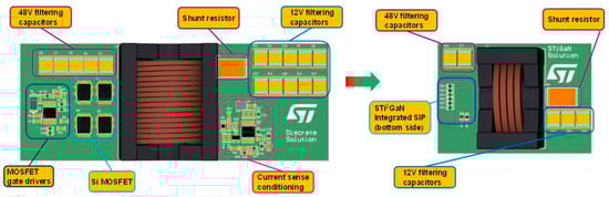
Figure 1.
Area reduction by increasing the switching frequency.
The total cost of the power converters can be estimated by considering the costs of passive components, PCBs, and power switches. Table 1 reports a comparison of the total cost when Si and GaN solutions are adopted. While there is not a substantial cost difference in the overall cost, the GaN-based power converter enables a strong efficiency improvement making it the best solution from a sustainability point of view.
Nowadays, the production and development costs of complex systems in GaN are the weak point of this technology [47,48]. The production, however, progresses and the high efficiency guaranteed by the material motivates large investments in this sector. From the market forecasts it is possible to observe the trend of reduction of the production costs of the GaN-based systems. Figure 2 shows the trend of the costs of realization of power devices in silicon and GaN. The maturity of the production process of silicon devices allows for obtaining large volumes of production at very low costs, ensuring competitive prices for complete systems. Unlike this, the production of devices in GaN has not yet reached the same levels of production maturity and yield, producing the highest costs for a single die. Mass production forecasts for GaN devices show that the cost for each device will drop below the silicon counterpart after 2026, while, as previously highlighted, the overall cost of the complete systems in Si and GaN devices is similar. More specifically, considering the bars in Figure 2, the first value in green (100%) represents a normalized (reference) cost for a Si-based 3 kW 48 V-to-12 V converter in 2019. The white bar next to it (12%) represents the portion due to the Si MOSFET cost. At that time, the overall cost of a similar converter using GaN technology was 25% larger as apparent from the first orange bar (125%). In this case, the contribution of the GaN HEMT to the overall cost was about 40% (white bar). Nowadays, the overall cost of the converter is reduced by about 10% in comparison to the reference case regardless of the use of an Si MOSFET (green bar equal to 90%) or a GaN HEMT (orange bar equal to 89%). Therefore, the current strong reduction of the GaN HEMT is enough to make the GaN-based converter cost comparable to the Si counterpart, although the impact of the GaN HEMT on the overall cost (20%) is still larger than the Si MOSFET (10%). The future reduction of production costs together with lower system costs will push the design and development phase to consolidate the transition to high frequency, preferring the GaN technology to the silicon one. Therefore, nowadays GaN technology is the best from a sustainability point of view while it is equivalent to Si one in terms of the overall cost of power electronics converters, while in the incoming years, the GaN technology will completely outperform the latter, especially in the field of electrified vehicles. In fact, both the high voltage segment of the HEV/EV market and the low voltage area for mild hybrid systems can benefit from this disruptive performance enhancement of the GaN technology especially under hard switch working conditions at high frequency.
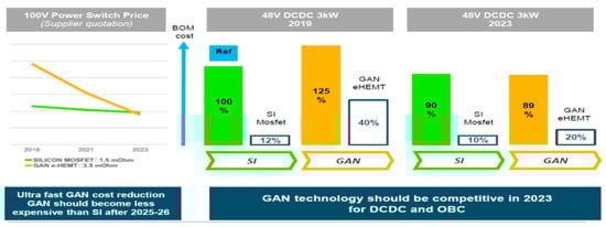
Figure 2.
Estimated cost production trend up to 2026.
Multiphase interleaved bidirectional buck–boost DC–DC converter can work up to 500 kHz–1 MHz in 48/12 V energy transfer systems. Moreover, also the insulated low-power flyback that feeds the gate driver can be integrated by a monolithic GaN device: controller and power switch. State-of-the-art products can address all those segments with a p-gate technology solution suitable for realizing smart and integrated solutions.
However, one of the main challenges in adopting the GaN HEMT is due to the aforementioned fast switching that requires a proper design and development of the board layout. More specifically, with rising edges faster than 5 ns, reducing the PCB parasitic inductances, in both driving and commutation loops, is fundamental. In this perspective and more in general to improve the performance (efficiency, electromagnetic interferences, and so on) of GaN-based converters some pieces of advice are provided in the following.
- The GaN HEMT and its driver must be placed close to each other to reduce parasitic inductances and the probability of electromagnetic interference that may affect the control signals of the power switches.
- The use of multi-layer PCB with very small vertical connections avoids loops, thus minimizing the parasitic inductances, especially in the driving path.
- Connecting each layer by copper vias for current forefront and return paths through big copper plates (noise shielding effect) concurrently to act as an efficient heatsink cooling down the device.
- The bulk and bypass capacitances must be placed close to the GaN HEMT and driver to stabilize the voltages and reduce the loop traces.
With this in mind, in the following sections, the performance of the state-of-the-art GaN HEMTs has been experimentally analyzed in different automotive applications. The devices used in this paper belong to the STi2GaN family (Table 2), which is a system-in-package solution that integrates a power stage with gate drivers, protections, and diagnostic functions. This monolithic solution is based on a normally off device presenting a p-GaN gate structure.
In particular, the devices used in Section 3 and Section 5 present a 100 V breakdown, and they integrate two or four dice in the same switch. In Section 4, the system integrates a GaN HEMT, presenting a 650 breakdown, with additional internal logic blocks. As a result, the device is capable of protecting itself from overcurrent and overtemperature events and sending diagnostic information to an external microcontroller. An advantage of the integration is the opportunity to turn off the GaN HEMT with zero gate-source voltage, thus ensuring a reduction of the losses caused by the third quadrant conduction during the dead time, and increased turn-on slew rate capability.
3. The 48–12 V DC–DC Converter in Mild Hybrid Applications
Today, due to the increasing attention paid to emissions reduction and the research of alternative solution for the automotive environment, car electrification both with hybrid and mild hybrid solution are getting more and more popular. The mild hybrid represents a good compromise being the simplest and basic solution for a transition from a combustion engine to a hybrid one. The mild hybrid solution combines a combustion engine and an electric motor to improve fuel economy and reduce emissions. Based on the BSG block, the startup is guaranteed by the combustion engine, and, thanks to the belt, the battery can be recharged, allowing the engine to be turned off whenever the car is coasting, braking, or stopped, and then quickly restarted once power is again required. The power flow can be reversible and thus there is a dedicated battery or energy storage during the recovery phase. The three main blocks are: a starter, a battery (Li-Ion), and dedicated management software, see Figure 3. The system can work at 48 V or 12 V, but a 48 V mild hybrid solution is preferred to reduce the current needed and to reduce the total power dissipation due to the heating of the wires. When the electric motor works, it provides additional energy to the engine. This solution guarantees lowering consumption and emissions.
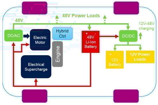
Figure 3.
Mild hybrid block diagram.
In this scenario, the 48/12 V conversion block is fundamental to recharge the 12 V battery and to supply the 12 V power loads, i.e., car accessories such as climate control, navigator, etc. Moreover, the converter can work bidirectionally thus recharging, when needed, the 48 V main battery of the system. A mild hybrid solution requires power conversion systems with high efficiency and high power density. High bandgap devices such as the GaN HEMTs are the best alternative to silicon for this application. The mild hybrid market requires intelligent and flexible systems that manage high currents. An interleaved structure is useful to achieve these targets. The first step to developing a multiphase buck converter for a mild hybrid environment is the realization of a single-phase converter based on the new emerging GaN technology. In particular, the activities consisted in designing a buck converter demo board properly realized to work with GaN technology and thus focusing on board layout design.
Due to the high switching frequency of the GaN power stage, all the connections, and in particular the driving loops, have been designed to minimize parasitic inductances which could lead to undesired turn-on and, consequently, potential failure due to cross-conduction. The basic circuit topology of a synchronous buck converter is shown in Figure 4 where both S1 and S2 are the power GaN switches. In the following subsections, some 48/12 V conversion systems will be discussed. They are in order of increasing complexity and integration level.
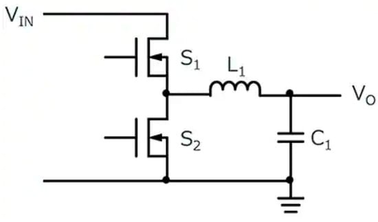
Figure 4.
Basic circuit of a buck converter.
3.1. Single-Phase Buck Converter
This section presents a basic 48/12 V converter realization. In particular, a single-phase converter has been developed and tested. Figure 5 shows the top view layout of the demo board which is based on an external driver and a monolithic GaN-based power stage, thus realizing in a single block both S1 and S2 switches. The main features of the converter are:
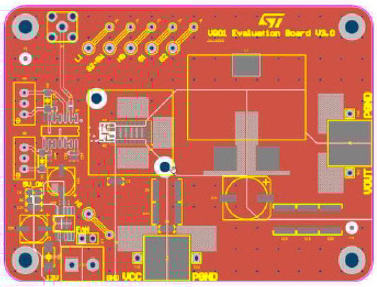
Figure 5.
Top layer of the single-phase buck converter demo board.
- -
- Input voltage 48 V;
- -
- Switching frequency, 500 kHz up to 1 MHz;
- -
- Duty cycle equal to 25% to obtain the desired 12 V output voltage;
- -
- Coil inductance 1.25 μH.
The last value is a compromise between the application power level and the switching losses due to the current peak. Different values have been considered, when L = 1.25 μH the best performance has been achieved at 500 kH. Moreover, a dedicated heatsink has been used to realize the cooling of the GaN samples.
The main switching waveforms experimentally obtained are shown in Figure 6. In particular, the waveforms are: Vds,LS (i.e., drain-source voltage of S2) is the purple trace, Vgs,LS (i.e., gate-source voltage of S2) is the green trace and Vgs,HS (i.e., gate-source voltage of S1) is the yellow trace. The measurements were executed at 20 A current load by using an electronic load. In particular, the equipment used is a power supply Agilent 6032 A, a GW INSTEK GPS-3303 power supply, an active load Croma 6314, a power meter YokoGawa WT310E, an oscilloscope Lecroy HDO6054A 500 MHz bandwidth with passive voltage probe LeCroy P4100, a Tektronix AFG3022B signal generator, a Multimeter fluke45.
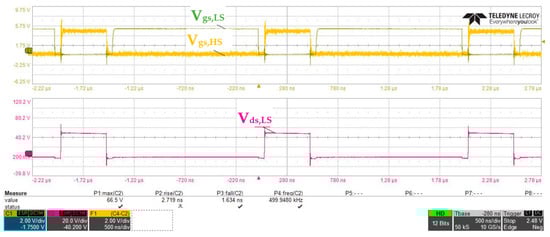
Figure 6.
Main switching waveforms at 20 A load.
The GaN power stage has been analyzed up to 50 A load current resulting in an overall efficiency of 95% in the flat range, middle load area, see Figure 7.
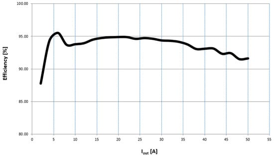
Figure 7.
Efficiency at 500 kHz over current load.
3.2. Interleaved Synchronous Buck Converter Controlled with a Microcontroller
The synchronous rectification technique is often used to improve the overall system efficiency. This solution replaces the diode with an active switch to avoid the conduction losses of the diode, thus reducing the power losses of the converter. In this context, the adopted buck converter with two active switches is implemented in a monolithic chip. Starting from the good results achieved with a single-phase converter, a three-phase interleaved structure has been chosen to maximize the overall system efficiency. This structure provides better results in terms of efficiency compared to the previous one. With a three-phase system, it is possible to shift the peak efficiency of the single-phase converter to a higher current value. Figure 8 and Figure 9 show the circuit schematic for a three-phase synchronous buck converter and the evaluation board.
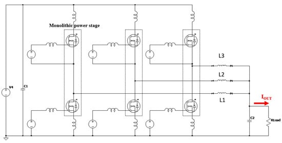
Figure 8.
Schematic of a three-phase synchronous buck converter.
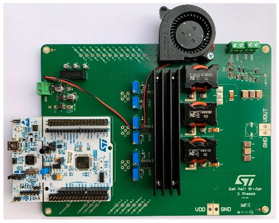
Figure 9.
Evaluation board of the converter.
The PWM signals and their phase shift are managed by the microcontroller STM32 Nucleo—F401RE. The complete system works at a 500 kHz switching frequency. The microcontroller also implements the closed-loop control of the converter. For duty cycle regulation the output voltage of the converter must be measured for modulation of the on-time amplitude of the three-phase PWM signals. The acquisition of the output voltage is performed by using a voltage divider with a 1:3 ratio and the information is provided to an ADC channel of the microcontroller. The over-current protection feature is useful to maximize system security. This function allows stopping the system when a peak of current occurs due to a short circuit or a failure of some devices. In the proposed converter, a shunt resistor sensor circuit is used for over-current valuation. In Figure 10 the main blocks are reported.
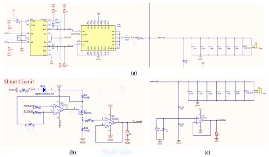
Figure 10.
Converter blocks: (a) driving, power stage, inductor, shunt resistor, and output capacitors; (b) shunt resistor sensor circuit; (c) duty cycle regulation circuit.
A test bench has been equipped with a 64 Xi 600 MHz Le Croy Oscilloscope and PP-005 Le Croy 500 MHz passive probes to view the drain-source voltage and current waveforms. The Agilent 6012B DC Power Supply has been exploited to supply the gate driver’s circuitry, while an active load is emulated by a Chroma 63,101 DC Electronic Load. A Yokogawa WT210 Digital Power Meter has been used to estimate the power conversion efficiency, a Fluke 45 Dual Display Multimeter has been used to view the output voltage, GW INSTEK GPS-3303 power supply has been exploited to supply (Vin) the converter.
To reduce the oscillations and the related power losses, the testing points have been designed to use passive probes equipped with pigtails and ground contact. This particular type of probe minimizes the loop between the testing point of interest and the ground, and it is recommended for high-frequency applications.
The converter has been powered with two different voltages. A 12 V power supply for logic and gate driver block and a 48 V power supply for the power stage. In this case, the three PWM signals have been generated with an STM32 Nucleo 401RE microcontroller to make the system more versatile. The dead time has been generated through an appropriate dead time circuit realized with a 74VHC132 QUAD 2-INPUT SCHMITT NAND GATE. Two gate drivers LMG1205 have been used to drive the GaN half-bridge. The gate drivers must be placed as close as possible to the half-bridge devices to reduce the parasitic inductances and any interference that could be generated. The gate resistance has been set to zero to maximize the switching speed. The LC filter has been properly designed to reduce the output voltage oscillation using a capacitor (36.6 μF) and an inductor (1 μH).
The switching behavior of the three phases system with the proper phase shift between each leg is shown in Figure 11.
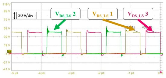
Figure 11.
VDS for the low side of each leg of the three-phase converter, with the proper phase shift.
This phase shift was externally set by using the microcontroller and it is highlighted by VDS waveforms. In this way, the system is completely autonomous, releasing from the function generators.
Figure 12 shows the three-phase currents, the voltage at the switch node for phase two, and the total current at the common node of the three inductors expressed as the sum of the three currents.
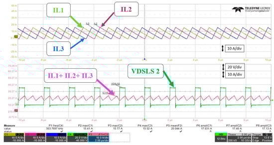
Figure 12.
Phase current waveforms for each leg and total output current waveform at 20 A load condition.
The use of the three interleaved phases has allowed for obtaining a peak efficiency of 95% for current values between 20 and 30 A (Figure 13). In this case, the portion of the power losses due to the GaN device is in the range of 15–30% (it depends on the load condition). This topology allows the maximization of the peak efficiency of a single-phase system bringing it to higher load conditions.
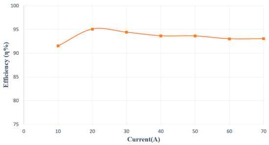
Figure 13.
Efficiency curve of three phases interleaved system.
The use of the microcontroller has also made the system more versatile. The management of the driving of the phases, in fact, has been carried out with only lines of code, without the aid of external function generators. The microcontroller has, moreover, appropriately managed the regulation of the duty cycle of the phases and the detection of the overcurrent events. Starting from these features it has been possible to create a self-regulating system to maintain the output voltage in the target values.
3.3. Bidirectional Interleaved Synchronous Converter
This section presents a multiphase interleaved buck–boost converter based on a 100 V asymmetric monolithic GaN half-bridge power stage, controlled by an innovative BCD9s-based controller properly developed to implement a closed-loop solution.
Figure 14 shows a three-phase buck converter with the main circuit blocks for converter driving, control, and safety. In particular, all the phases are realized by a traditional single-phase buck with a driving block and a dedicated coil. The safety switches are fundamental in case of overvoltage events both in the input or output stage. The control unit communication is based on SPI protocol. The current sense is realized through a shunt resistor directly connected to the driver.
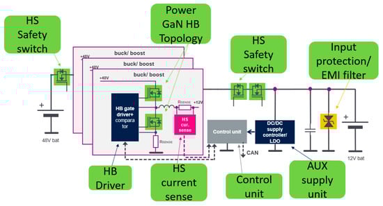
Figure 14.
Block diagram of interleaved 48–12 V converter.
Based on a double control loop, (first) current and (then) voltage are used to regulate the output voltage. A strength of the system is its very high level of integration obtained by realizing a system in package (SiP) solution that integrates the power stage and control unit in the same package. To ensure high performance, integration is mandatory to minimize the stray inductances of the connection in the power path. The SiP solution allows the integration of those connections avoiding, in this way, the possible current and voltage ringing, which are the main root of failure for GaN devices, especially in discrete solutions.
The main features characterizing the proposed smart converter are the ability to switch from a single-phase topology to an interleaved one if higher current management is required, achieving 6-phase maximum operation to manage about 75 A output current per phase and overall, 250 A.
A full evaluation of the new GaN-based 48–12 V converter solution has been carried out on a dedicated demo board, according to the schematic shown in Figure 14. The converter is mainly composed by the following components.
- Tiny chorus board (motherboard) allocates the µC
- DC/DC converter demo board (daughter board)
- GUI (graphical user interface)
- SW on microcontroller
The main parameters are:
- VIN = 48 V
- L = 1.25 µH
- Fsw = 500 kHz (up to 1 MHz)
- Rshunt = 1 mΩ
The duty cycle is internally set by the controller to guarantee the desired VO.
Figure 15 shows a picture of the demo board realized with the SiP solution integrating both the controller and power stage. To easily set the parameters, a GUI has been developed and installed on a personal computer that communicates with the microcontroller board by means of a USB port, while the communication between the microcontroller board (mother) and DC/DC one (daughter) is realized using the SPI protocol.
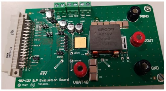
Figure 15.
Evaluation board of the interleaved 48–12 V converter.
Some fundamental features of the component are its overtemperature and short circuit protections which makes the device turn off when necessary.
The measurements were executed at 20 A current load by using an electronic load. In particular, the equipment consists of: a power supply Agilent 6032 A, a GW INSTEK GPS-3303 power supply, an active load Croma 6314, a power meter YokoGawa WT310E, an oscilloscope: Lecroy HDO6054 A 500 MHz bandwidth with passive voltage probe LeCroy P4100, a Tektronix AFG3022B signal generator, a Multimeter fluke45.
As an example of the converter evaluation at 500 kHz frequency, the switching waveforms in Figure 16 and Figure 17 show the ability of the system to dynamically switch from a current setpoint to another and to regulate the output at a desired voltage level with extremely good waveforms on the power stage. The power stage has very fast switching, in the range of a few ns with limited voltage spikes. In particular, Figure 16 shows the main switching waveforms when changing the current setpoint from 0 A to 8 A (about 100 ns settling time) and Figure 17 shows the switching waveforms in voltage regulation control mode realized by using a constant resistance on the output. In this case, the waveforms are: red line for output current (5 A/div), yellow line for switching node (10 V/div), purple line for output voltage (10 V/div), blue lines for VGS high side and low side (5 V/div).
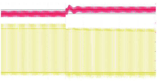
Figure 16.
Dynamic current regulation in buck mode operation from 0 A to 8 A. Red line for IOUT (20 A/div) and yellow line for VDS low side (10 V/div).
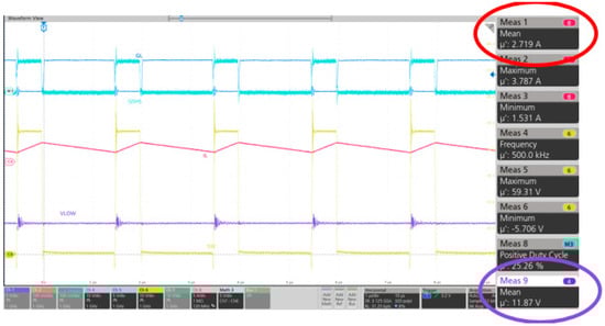
Figure 17.
Voltage control loop operation. The red circle highlights the mean current flowing through the inductor while the purple one shows the mean value of the output voltage which follows the desired setpoint.
4. Onboard Chargers for Plug-in Hybrid- and Full-Electric Applications
The increasing demand in the vehicle electrification field is leading to the fast development of power electronics systems suitable for battery charge. In particular, both in plug-in hybrid and full electric applications, one of the most important blocks is the onboard charger (OBC), used to physically convert the AC power coming from the external source into DC power useful to charge the HV battery of the vehicle. A simple block schematic of a general OBC is shown in Figure 18. The main blocks are a diode voltage rectifier, which could be a simple diode bridge topology or a more complex one, a power factor corrector and an insulated high voltage dc/dc converter to effectively charge the 400 V battery.

Figure 18.
Block scheme of OBC architecture.
In this scenario, gallium nitride technology gives its high contribution in terms of high switching performances and high system efficiency achievable.
This paper shows an HV boost converter solution able to guarantee a 400 V output voltage starting from a 200 V input. The target switching frequency for the application is 300 kHz, thus making the GaN device the best choice. Figure 19 shows the circuit schematic of a traditional synchronous boost converter.
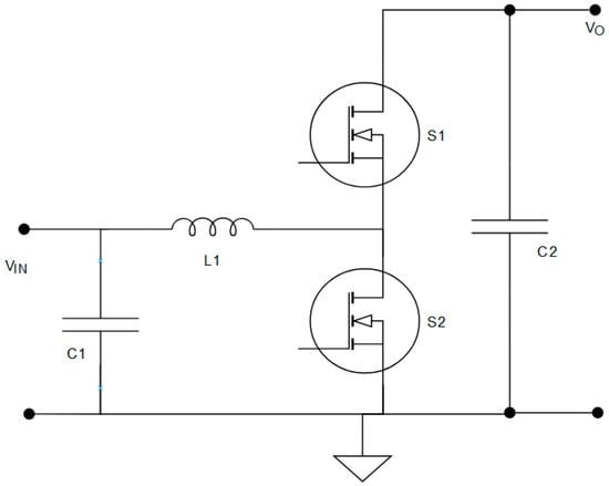
Figure 19.
Basic circuit schematic of a boost converter.
4.1. Microcontroller-Based Closed Control Loop Asynchronous Boost Converter for Onboard Charger
The adopted GaN platform allows the integration in a monolithic chip the driver circuitry with embedded some protections and the GaN power switch. Properly designed for the automotive environment, a 650 V monolithic power with embedded power stage and overcurrent and overtemperature protections, housed in an innovative bond wire-free package, Direct Copper Interconnected Pack (DCI Pack), has been developed and analyzed to realize a high voltage boost converter for OBC.
The main features of the system are an input voltage, VIN, equal to 200 V, a desired output voltage, VO, of 400 V, and thus a duty cycle equal to 50%. The switching frequency was set to 300 kHz as a compromise between fully exploiting the performance of the GaN device and limiting the switching losses. Based on the previously described monolithic IC solution, a closed control loop synchronous boost converter based on STM32 microcontroller has been designed and developed and the main testing results will be shown in the following sections. In order to achieve a high-power level, the converter has to work in CCM.
An innovative aspect is the use of the microcontroller for the closed-loop management of a high-frequency power conversion system. An STM32 microcontroller, based on Nucleo-STM32G474RE, dynamically regulates the operating conditions of the power stage depending on the load. This system includes some protective features to stop the driving stage in case of failure. The closed-loop control acts through an accurate reading of the input and output voltage levels realized by exploiting two optocouplers. By forcing a current on the anode of the LED, a proportional current is produced on the collector of the output BJT, which is connected to a 3.3 V point. The voltage on the output collector is then read by the ADC of the MCU.
The tests were performed by using an output electronic load set in constant voltage mode. The tests aim to realize the desired voltage conversion from 200 V input to 400 V output voltage. The system can work with a very stable control loop and achieve the hard switching condition by exploiting a 20 μH coil and working at a 300 kHz switching frequency. The system has been tested up to 2 kW output power and 300 kHz switching frequency resulting in an overall efficiency of 98% (Figure 20).
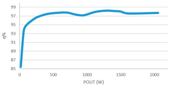
Figure 20.
System efficiency at 300 kHz switching frequency.
Figure 21 shows the OCP and OTP protections which, respectively, induce the permanent and the temporary turn OFF and the part by avoiding destruction when the threshold is exceeded. In particular, Figure 21a shows the triggering of OCP which permanently turns the device off when the current threshold is overcome. While Figure 21b shows the triggering of OTP when the temperature overcomes 180 °C. Once the OTP is triggered, the device latches till the Diag_T signal drop achieves back the minimum threshold so that it starts back to switch at the target conditions. If the over-temperature is still present, the cycling operation mode continues until the average device temperature drops back under 175 °C. In both pictures the purple lines represent the low side VDS (100 V/div) while the blue lines represent the coil current (10 A/div) whose mean value is the input current, the green line is the overcurrent protection diagnostic pin (5 V/div), while the dark blue is the over-temperature protection one (5 V/div)
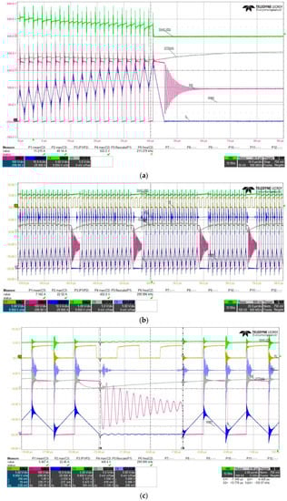
Figure 21.
Protections effect—(a) OCP, (b) OTP, (c) OTP sub-interval magnification.
4.2. Power Factor Correction Interleaved Boost Converter Onboard Charger
Exploiting the advantages of the monolithic GaN technology, a high-efficiency boost converter PFC has been designed and a demo board has been realized. Experimental tests have shown a 98% efficiency under 1.5 kW output power while the converter is driven at 300 kHz.
As already mentioned, the system is designed to work as a power factor correction stage for onboard chargers of battery electric vehicles (BEVs) and plug-in hybrid electric vehicles (PHEV). Thus, it operates a 200 V–400 V input-to-output conversion with a maximum target of 1.5 kW power output. The use of a dual-phase interleaved topology allows the converter to have almost-zero output current ripple at the boundary condition, which is a huge benefit when it comes to battery charging systems. Taking advantage of a new monolithic GaN HEMT technology, that integrates a 30 mΩ power device with a driver and protections in a single die, the converter switches at 300 kHz while minimizing the need for dedicated driving circuitry. As can be seen from the full schematic shown in Figure 22 the two power devices need an auxiliary 15 V supply and some external components to ensure that they operate as expected. In particular, the 6 V Zener diode D3 allows a stable supply voltage for the internal driver, VDD. The C6-R4-C7 network on the VDD pin regulates the turn-on slew rate of the VDS voltage (60 V/ns). On the IN pin, the R9-C9 network allows smoothening of the driving PWM signal.
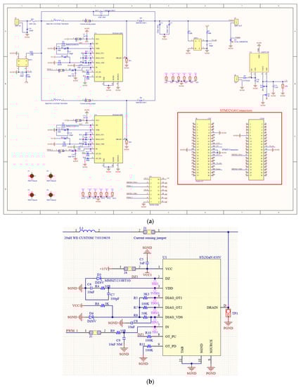
Figure 22.
Interleaved boost converter PFC: (a) schematic; (b) detail of the implementation of the power devices.
The driving of the two phases is managed by an STM32 microcontroller, which embeds—among the others—a high-resolution timer with a 184 ps time-step that allows to finely control the PWM duty cycle, five 12-bit ADCs capable of 4 Msamples/s sampling rate, seven 12-bit DACs at 15 Msamples/s, seven fast comparators and six op-amps with PGA function, whose inputs and outputs can be connected to the ADCs or DACs, respectively.
Thanks to these features, the use of optocouplers, and a dedicated software PID algorithm, it has been possible to implement a precise and effective control loop for output voltage regulation.
After the design process, a prototype board of the converter, shown in Figure 23, has been realized and experimentally analyzed. Figure 24 shows the complete experimental setup.
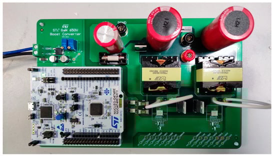
Figure 23.
Interleaved boost PFC demo board.
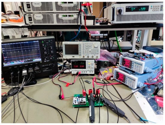
Figure 24.
The experimental setup used to perform the tests.
The experimental setup consists of the following components.
- -
- TDK-Lambda GEN600-5.5 DC power supply. It can provide a maximum of 600 V and 5.5 A DC. Due to the higher input current needed, two of these have been connected in parallel in a master–slave configuration, allowing to double the nominal output
- -
- ITECH IT8322 regenerative DC electronic load. It can be programmed for constant voltage, current, resistance or power, and can absorb a maximum of 800 V, 40 A, or 7 kW
- -
- GW Instek GPD-3303D DC power supply. Provides a maximum output of 30 V and 3 A, used to supply the auxiliary 15 V input
- -
- Teledyne-LeCroy HDO8058A 500 MHz high-definition oscilloscope, with 8 analog and 16 digital channels, 12-bit resolution and 10 GS/s sampling rate
- -
- Yokogawa WT310EH Digital Power Meter. It covers input current values from 40 mA to 40 A RMS, and can work both in DC and AC. Two of these have been put on the input and output of the board, to take efficiency measurements.
Several tests were performed at 150 V–300 V input–output voltage under different load conditions, with 100 W steps to evaluate efficiency as a function of the output power.
Figure 25a shows the behavior of the converter at 1.5 kW output power, with a focus on a single switching period in Figure 25b. The converter works slightly in DCM, with a duty cycle close to 50%, thus approaching the boundary condition. Oscillations can be seen on the two switching nodes, starting from the phase inductors’ currents zero-crossing. Because the currents lead the respective switching node voltages, this behavior can be explained by the discharging of the output capacitance of the power devices, which triggers a resonance between the phase inductors and the capacitance itself.
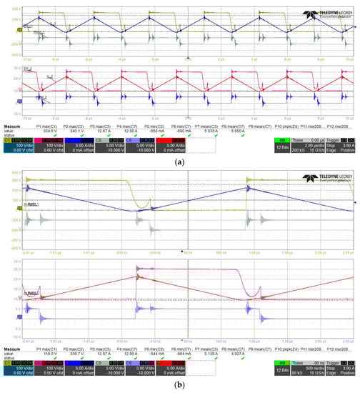
Figure 25.
Waveforms for POUT = 1.5 kW. (a) Main waveforms (yellow and purple traces are, respectively, the VDS of the two power devices, red and blue traces are the inductors currents, grey and light blue traces represent the two driving PWM signals; (b) magnification of a single period.
Figure 26a,b show the measurements of the VDS ringing frequency and overshoot amplitude, being equal to 65.8 MHz and 34 V (11% overshoot), respectively. From the frequency measurement, considering an output capacitance in the tens of nF range, the PCB stray inductance order of magnitude is tens of nH.
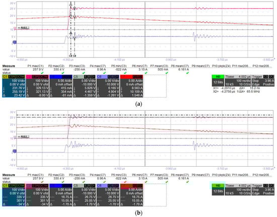
Figure 26.
VDS measurements (yellow and purple traces are, respectively, the VDS of the two power devices, red and blue traces are the inductors currents, grey and light blue traces represent the two driving PWM signals): (a) ringing frequency at turn-off; (b) overshoot amplitude at turn-off.
The efficiency plot, in Figure 27, shows how at low load the switching losses play an important role and cause a drop in efficiency. As the output load increases, their influence becomes less graving while conduction losses are limited thanks to the low RDS(on) of the two switches, allowing them to reach a peak efficiency of around 98%.
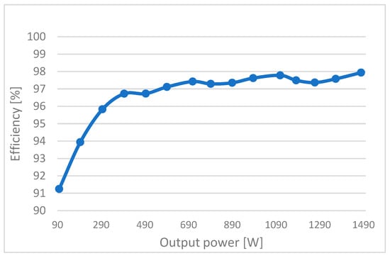
Figure 27.
Efficiency plot vs. output power.
5. Wireless Charging System for Automotive Applications
Among the most diffused applications of wireless power transfer (WPT), smartphone wireless chargers have been gaining more and more attention. Traditionally these kinds of applications are based on silicon. However, gallium nitride is the new emerging candidate, used to replace Si technology, thanks to its notable performance, especially in terms of high switching speed, low switching losses, very high operation frequency, and, consequently, good power density. The charger exploits a GaN-based monolithic full-bridge, which enables the aforementioned advantages introduced by GaN and guarantees a high level of reliability, to make the application suitable for the automotive environment. The proposed system works at low frequency, according to the rules imposed by the Qi protocol. The monolithic nature of the power converter allows for drastically reducing the H-bridge current and voltage spikes and further improves the ability to work at very high operating frequencies. Another innovation introduced is represented by the rectification block on the receiver side which is characterized by a self-driven approach.
Figure 28 shows the general block system of the resonant WPT system with a series–series (SS) compensating network. The main blocks are the resonant tanks, which need to be sized to resonate at the same resonance frequency. Thus, the following equations must be satisfied:
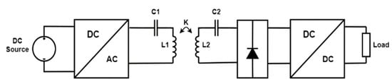
Figure 28.
Block diagram of resonant WPT system.
With
The loss minimization is obtained when the converter works in the inductive load region. The switching frequency of the inverter has to be higher than the resonance frequency to work in this region.
The development of a wireless charger for mobile phones requires that the system complies with the Qi protocol. This protocol imposes a working frequency in the range of 100–200 kHz. Moreover, the baseline profile establishes an output power level of 5 W. By choosing a resonance frequency of 100 kHz, a switching frequency of the GaN full-bridge in the range allowed by the Qi protocol, and by selecting a transmitter and a receiver coil, respectively, L1 = 24 µH and L2 = 7.5 µH, by exploiting the inverse of formulas (1) and (2), the compensation capacitors values have been found: C1 = 100 nF and C2 = 330 nF. One of the main particularities of the proposed wireless charger is the use of a monolithically integrated full-bridge inverter, based on GaN devices. The monolithic nature of the inverter allows a notable reduction of the losses as a consequence of the lower gate-source and drain-source oscillations and voltage and current stresses, with the following great reduction of the EMI components. In particular, the full bridge used is a 100 V breakdown voltage and extremely low RDSon (22 mΩ) monolithic converter.
The rectification block consists of a bridge structure where the devices at the top are Schottky diodes and the devices at the bottom are Si power MOSFETs. The particularity is the self-driven nature of the developed rectifier, in which the two gate terminals of the MOSFETs are directly connected to the resonant tank, as shown in Figure 29. During the positive half-wave D1 conducts while D2 is OFF and, at the same time, the gate-source voltage of M2 is high enabling, in this way, the switch conduction. Similarly, in the other half period, diode D2 is ON and switch M1 sees a high voltage at its gate-source terminals, thus allowing the switch conduction. Two Zener diodes, placed back-to-back, have been inserted between the gate terminals of M1 and M2 and ground to avoid excessive voltage spikes that can cause the undesired break of the devices. The proposed solution constitutes a compromise between the cost of the rectifier and its efficiency. The lower power losses of the self-driven solution derive from the lower drain-source voltages of the switches compared to the forward voltage of the diodes.
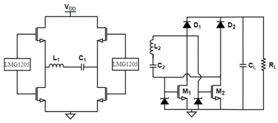
Figure 29.
Basic circuit of wireless charger with self-driven rectifier.
The measurements were executed by using an electronic load. In particular, the equipment used is: a power supply Agilent 6032A, a GW INSTEK GPS-3303 power supply, an active load Croma 6314, a power meter YokoGawa WT310E, an oscilloscope: Lecroy HDO6054A 500 MHz bandwidth with passive voltage probe LeCroy P4100, a Tektronix AFG3022B signal generator, a Multimeter fluke45.
Some experimental tests have been executed on the prototype shown in Figure 30.
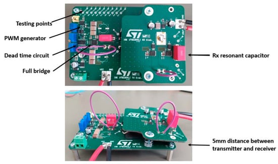
Figure 30.
Top and side view of the wireless charger demo board.
A voltage supply equal to 10 V has been used. An equivalent bypass capacitor of 14µF has been placed between the voltage generator and the ground. A 45 ns dead time has been inserted and a PWM signal with 5 V amplitude has been chosen. All the results of the tests have been obtained by neglecting the LDO block and by considering an output capacitor of 50 µH. Figure 31 shows the switching waveforms of the full bridge GaN devices. In particular, the purple line is the VDS of the low side device (5 V/div), the blue line and the yellow one are, respectively, the LS and HS GS voltages (5 V/div) and the green line is the output current (1 a/div). As can be seen, the switching waveforms of the converter are very clear without any spurious peak oscillations and overvoltages meaning very low power losses, cross-conduction probability, and EMI components of the monolithic solution.
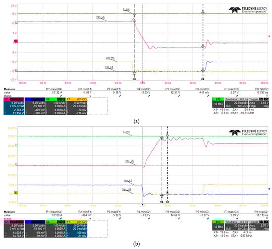
Figure 31.
Switching waveforms of the converter using the monolithic device: (a) turn-off, (b) turn-on.
Figure 32 reports the power transfer efficiency at different load conditions. It is clear that the proposed solution presents a higher efficiency for all load conditions. The highest efficiency (85%) is achieved with a load equal to 10 Ω, while the highest difference between the two solutions is achieved at a load condition of about 5 Ω. Because the application aims to provide 5 W to the receiver, given as 5 V and 1 A, the operating point of interest is exactly 5 Ω. Thus, there is a good improvement in efficiency compared, for example, to the GaN-based monolithic solution with a diode bridge rectifier which presents a maximum efficiency of 75%, see Figure 32.
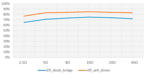
Figure 32.
System efficiency vs. load variation.
6. Conclusions
This paper has analyzed the impact of GaN in the automotive sector from the costs and sustainability points of view. The analysis has highlighted that today, the reduction in passive components cost obtained using GaN HEM compensates for the higher cost of the device in comparison with Si solutions. Hence, currently, there is no substantial difference in the overall cost when using Si or GaN in key and widely adopted automotive applications, such as 48 V–12 V converters and onboard chargers, as well as in emerging applications, such as wireless chargers.
The efficiency of these power converters is even more and more important considering that more power is necessary to satisfy the increasing vehicle digitalization, including assisted driving solutions, the adoption of sensors and devices enabling the Internet of Things and artificial intelligence solutions. Good efficiency is essential for a sustainable future since it increases the mileage covered thus increasing people’s confidence in electric transportation and also it reduces the wasted power due to the converter power losses. In this perspective, some GaN-based solutions in the aforesaid automotive application are presented, thus highlighting the high efficiency achievable thanks to GaN devices.
Author Contributions
Conceptualization, F.S.; Methodology, S.M.; Software, S.A.R.; Validation, F.C., G.D. and G.N.; Investigation, F.C., G.D. and G.N.; Data curation, F.C., G.D. and G.N.; Writing—original draft, F.C., G.D., G.N. and S.A.R.; Writing—review & editing, S.M. and S.A.R.; Supervision, F.S. and S.A.R.; Project administration, F.S. All authors have read and agreed to the published version of the manuscript.
Funding
This research was partially funded by Ministry of Education, Universities and Research (Italy) under the call PRIN 2017 grant number 2017MS9F49.
Data Availability Statement
The data is reported in the manuscript.
Conflicts of Interest
The authors declare no conflict of interest.
References
- Mihet-Popa, L.; Saponara, S. Toward Green Vehicles Digitalization for the Next Generation of Connected and Electrified Transport Systems. Energies 2018, 11, 3124. [Google Scholar] [CrossRef]
- Umezawa, Y.; Yamauchi, K.; Seto, H.; Imamura, T.; Namerikawa, T. Optimization of fuel consumption and NO x emission for mild HEV via hierarchical model predictive control. Control. Theory Technol. 2022, 20, 221–224. [Google Scholar] [CrossRef]
- Khamesipour, M.; Chitsaz, I.; Salehi, M.; Alizadenia, S. Component sizing of a series hybrid electric vehicle through artificial neural network. Energy Convers. Manag. 2022, 254, 115300. [Google Scholar] [CrossRef]
- Saponara, S.; Lee, C.H.T.; Wang, N.X.; Kirtley, J.L. Electric Drives and Power Chargers: Recent Solutions to Improve Performance and Energy Efficiency for Hybrid and Fully Electric Vehicles. IEEE Veh. Technol. Mag. 2020, 15, 73–83. [Google Scholar] [CrossRef]
- Hossain Lipu, M.S.; Miah, M.S.; Ansari, S.; Meraj, S.T.; Hasan, K.; Elavarasan, R.M.; Mamun, A.A.; Zainuri, M.A.A.M.; Hussain, A. Power Electronics Converter Technology Integrated Energy Storage Management in Electric Vehicles: Emerging Trends, Analytical Assessment and Future Research Opportunities. Electronics 2022, 11, 562. [Google Scholar] [CrossRef]
- Wang, J.; Wang, Q.; Jin, L. Modeling and simulation studies on differential drive assisted steering for EV with four-wheel-independent-drive. In Proceedings of the 2008 IEEE Vehicle Power and Propulsion Conference, Harbin, China, 3–5 September 2008. [Google Scholar] [CrossRef]
- Zhao, D.; Xia, Z.; Zhang, Q. Model-Free Optimal Control Based Intelligent Cruise Control with Hardware-in-the-Loop Demonstration [Research Frontier]. IEEE Comput. Intell. Mag. 2017, 12, 56–69. [Google Scholar] [CrossRef]
- Desai, M.; Phadke, A. Internet of Things based vehicle monitoring system. In Proceedings of the 2017 Fourteenth International Conference on Wireless and Optical Communications Networks (WOCN), Mumbai, India, 24–26 February 2017. [Google Scholar]
- Wei, H. Analysis on the Applications of AI in Vehicles and the Expectation for Future. In Proceedings of the 2020 5th International Conference on Information Science, Computer Technology and Transportation (ISCTT), Shenyang, China, 13–15 November 2020. [Google Scholar]
- Noussan, M.; Tagliapietra, S. The effect of digitalization in the energy consumption of passenger transport: An analysis of future scenarios for Europe. J. Clean. Prod. 2020, 258, 120926. [Google Scholar] [CrossRef]
- Bonfitto, A. A Method for the Combined Estimation of Battery State of Charge and State of Health Based on Artificial Neural Networks. Energies 2020, 13, 2548. [Google Scholar] [CrossRef]
- McQueen, B. Big Data Analytics for Connected Vehicles and Smart Cities; Artech House: Norwood, MA, USA, 2017. [Google Scholar]
- Bensrhair, A.; Bapin, T. Artificial Intelligence for Vehicles. In From AI to Autonomous and Connected Vehicles: Advanced Driver-Assistance Systems (ADAS); Wiley: New York, NY, USA, 2021. [Google Scholar]
- Faraci, G.; Grasso, C.; Schembra, G. Reinforcement-Learning for Management of a 5G Network Slice Extension with UAVs. In Proceedings of the IEEE INFOCOM 2019—IEEE Conference on Computer Communications Workshops, Paris, France, 29 April–2 May 2019; pp. 732–737. [Google Scholar]
- Grasso, C.; Raftopoulos, R.; Schembra, G. Smart Zero-Touch Management of UAV-Based Edge Network. IEEE Trans. Netw. Serv. Manag. 2022, 19, 4. [Google Scholar] [CrossRef]
- Khayyam, H.; Javadi, B.; Jalili, M.; Jazar, R.N. Artificial Intelligence and Internet of Things for Autonomous Vehicles. In Nonlinear Approaches in Engineering Applications; Jazar, R., Dai, L., Eds.; Springer: Cham, Switzerland, 2019. [Google Scholar]
- Xu, X.; Li, H.; Xu, W.; Liu, Z.; Yao, L.; Dai, F. Artificial intelligence for edge service optimization in Internet of Vehicles: A survey. Tsinghua Sci. Technol. 2022, 27, 270–287. [Google Scholar] [CrossRef]
- D’Amico, V.; Lombardo, A.; Melita, M.; Rametta, C.; Schembra, G. An SDN/NFV telco operator platform for video broadcasting. IEEE Commun. Mag. 2016, 54, 122–128. [Google Scholar] [CrossRef]
- D’Urso, F.; Grasso, C.; Santoro, C.; Santoro, F.F.; Schembra, G. The Tactile Internet for the flight control of UAV flocks. In Proceedings of the 2018 4th IEEE Conference on Network Softwarization and Workshops (NetSoft), Montreal, QC, Canada, 25–29 June 2018; pp. 470–475. [Google Scholar]
- ASheik, A.T.; Maple, C. Edge Computing to Support Message Prioritisation in Connected Vehicular Systems. In Proceedings of the 2019 IEEE Global Conference on Internet of Things (GCIoT), Dubai, United Arab Emirates, 4–7 December 2019. [Google Scholar]
- Leteinturier, P.; Mueller, C. Power Semiconductors—The Keys for a Future Green Mobility. In Proceedings of the 2020 32nd International Symposium on Power Semiconductor Devices and ICs (ISPSD), Vienna, Australia, 13–18 September 2020. [Google Scholar]
- Watts Butler, S. Enabling a Powerful Decade of Changes [Flyback]. IEEE Power Electron. Mag. 2019, 6, 18–26. [Google Scholar] [CrossRef]
- Shenai, K. High-Density Power Conversion and Wide-Bandgap Semiconductor Power Electronics Switching Devices. Proc. IEEE 2019, 107, 2308–2326. [Google Scholar] [CrossRef]
- Armando, E.; Fusillo, F.; Musumeci, S.; Scrimizzi, F. Low Voltage Trench-Gate MOSFETs for High Efficiency Auxiliary Power Supply Applications. In Proceedings of the 2019 International Conference on Clean Electrical Power (ICCEP), Otranto, Italy, 2–4 July 2019; pp. 165–170. [Google Scholar] [CrossRef]
- Marati, N.; Ahammed, S.; Karuppazaghi, K.; Vaithilingam, B.; Biswal, G.R.; Bobba, P.B.; Padmanaban, S.; Chenniappan, S. Recent Advancements in Power Electronics for Modern Power Systems—Comprehensive Review on DC--Link Capacitors Concerning Power Density Maximization in Power Converters. In Artificial Intelligence-Based Smart Power Systems; Wiley: Hoboken, NJ, USA, 2023. [Google Scholar]
- Singh, B. Novel and Ruggedized Power Electronics for Off-Highway Vehicles. IEEE Electrif. Mag. 2014, 2, 31–41. [Google Scholar] [CrossRef]
- Boutros, K.S.; Chu, R.; Hughes, B. GaN power electronics for automotive application. In Proceedings of the 2012 IEEE Energytech, Cleveland, OH, USA, 29–31 May 2012. [Google Scholar]
- Chen, J.; Nguyen, M.-K.; Yao, Z.; Wang, C.; Gao, L.; Hu, G. DC-DC Converters for Transportation Electrification: Topologies, Control, and Future Challenges. IEEE Electrif. Mag. 2021, 9, 10–22. [Google Scholar] [CrossRef]
- Lee, S.-R.; Choi, B.-Y.; Lee, J.-Y.; Won, C.-Y. 48 V to 12 V soft-switching interleaved buck and boost converter for mild-hybrid vehicle application. In Proceedings of the 19th International Conference on Electrical Machines and Systems (ICEMS), Chiba, Japan, 13–16 November 2016. [Google Scholar]
- Biswas, S.; Jones, E.A.; de Rooij, M.; Glaser, J.S. GaN-based High Current Bi-directional DC-DC Converter for 48 V Automotive Applications. In Proceedings of the PCIM Europe 2019; International Exhibition and Conference for Power Electronics, Intelligent Motion, Renewable Energy and Energy Management, Nuremberg, Germany, 7–9 May 2019; VDE: Nuremberg, Germany, 2019. [Google Scholar]
- Jones, E.A.; de Rooij, M.; Biswas, S. GaN Based DC-DC Converter for 48 V Automotive Applications. In Proceedings of the 2019 IEEE Workshop on Wide Bandgap Power Devices and Applications in Asia (WiPDA Asia), Taipei, Taiwan, 3–25 May 2019. [Google Scholar]
- Taube, J.; Panandikar, H.; Tippe, L.; Herzog, H.-G. MINLP Optimized Synchronous Buck Converter Using GaN-Transistors in 48 V/12 V Power Nets. In Proceedings of the 2019 IEEE Vehicle Power and Propulsion Conference (VPPC), Hanoi, Vietnam, 14–17 October 2019. [Google Scholar]
- Choi, M.; Jeong, D.-K. 18.6 A 92.8%-Peak-Efficiency 60A 48V-to-1V 3-Level Half-Bridge DC-DC Converter with Balanced Voltage on a Flying Capacitor. In Proceedings of the 2020 IEEE International Solid- State Circuits Conference—(ISSCC), San Francisco, CA, USA, 16–20 February 2020; pp. 296–298. [Google Scholar]
- Bendicks, A.; Rübartsch, M.; Frei, S. Active cancellation of periodic EMI at all terminals of a DC-to-DC converter by injecting multiple artificially synthesized signals. IEEE Electromagn. Compat. Mag. 2020, 9, 73–80. [Google Scholar] [CrossRef]
- Dini, P.; Saponara, S. Electro-Thermal Model-Based Design of Bidirectional On-Board Chargers in Hybrid and Full Electric Vehicles. Electronics 2021, 11, 112. [Google Scholar] [CrossRef]
- Dong, A.; Sadeghpour, D.; Bauman, J. High Efficiency GaN-based Non-isolated Electric Vehicle On-board Charger with Active Filtering. In Proceedings of the 2022 IEEE Transportation Electrification Conference & Expo (ITEC), Anaheim, CA, USA, 15–17 June 2022; pp. 1307–1313. [Google Scholar]
- Vu, H.-N.; Abdel-Monem, M.; El Baghdadi, M.; Van Mierlo, J.; Hegazy, O. Multi-Objective Optimization of On-Board Chargers Based on State-of-the-Art 650V GaN Power Transistors for the Application of Electric Vehicles. In Proceedings of the 2019 IEEE Vehicle Power and Propulsion Conference (VPPC), Hanoi, Vietnam, 14–17 October 2019. [Google Scholar]
- Bay, O.; Hosseinabadi, F.; Chakraborty, S.; El Baghdadi, M.; Hegazy, O. Multi-Objective Optimization of Bi-directional On-Board Chargers Based on 650V GaN Power Transistors. In Proceedings of the IECON 2022—48th Annual Conference of the IEEE Industrial Electronics Society, Brussels, Belgium, 17–20 October 2022. [Google Scholar]
- Martinez, W.; Lin, W.; Suarez, C. EMC Implications of Implementing WBG Devices in Battery Charger Modules for Electric Vehicles. In Proceedings of the 2022 International Power Electronics Conference (IPEC-Himeji 2022- ECCE Asia), Himeji, Japan, 15–19 May 2022; pp. 2516–2521. [Google Scholar]
- Qian, W.; Zhang, X.; Fu, Y.; Lu, J.; Bai, H. Applying normally-off GaN HEMTs for coreless high-frequency wireless chargers. CES Trans. Electr. Mach. Syst. 2017, 1, 418–427. [Google Scholar] [CrossRef]
- Bettini, A.; Cosnier, T.; Magnani, A.; Syshchyk, O.; Borga, M.; Decoutere, S.; Neviani, A. Analysis and Design of a Fully-Integrated Pulsed LiDAR Driver in 100V-GaN IC Technology. In Proceedings of the 2022 17th Conference on Ph.D Research in Microelectronics and Electronics (PRIME), Villasimius, Italy, 12–15 June 2022; pp. 273–276. [Google Scholar]
- Musumeci, S.; Barba, V.; Palma, M. GaN-Based Low-Voltage Inverter for Electric Scooter Drive System. In Proceedings of the 2022 AEIT International Annual Conference (AEIT), Rome, Italy, 3–5 October 2022. [Google Scholar]
- Meneghini, M.; De Santi, C.; Abid, I.; Buffolo, M.; Cioni, M.; Abdul Khadar, R.; Nela, L.; Zagni, N.; Chini, A.; Medjdoub, F.; et al. GaN-based power devices: Physics, reliability, and perspectives. J. Appl. Phys 2021, 130, 181101. [Google Scholar] [CrossRef]
- Musumeci, S.; Panizza, M.; Stella, F.; Perraud, F. Monolithic Bidirectional Switch Based on GaN Gate Injection Transistors. In Proceedings of the 2020 IEEE 29th International Symposium on Industrial Electronics (ISIE), Delft, The Netherlands, 17–19 June 2020; pp. 1045–1050. [Google Scholar]
- Musumeci, S.; Mandrile, F.; Barba, V.; Palma, M. Low-Voltage GaN FETs in Motor Control Application; Issues and Advantages: A Review. Energies 2021, 14, 6378. [Google Scholar] [CrossRef]
- Zhang, P.; Yang, S.; Xie, H.; Li, Y.; Wang, F.; Gao, M.; Guo, K.; Wang, R.; Lu, X. Advanced Three-Dimensional Microelectrode Architecture Design for High-Performance On-Chip Micro-Supercapacitors. ACS Nano 2022, 16, 17593–17612. [Google Scholar] [CrossRef] [PubMed]
- Lidow, A.; De Rooij, M.; Strydom, J.; Reusch, D.; Glaser, J. GaN Transistors for Efficient Power Conversion, 3rd ed.; John Wiley & Sons: Hoboken, NJ, USA, 2019. [Google Scholar] [CrossRef]
- Zhong, Y.; Zhang, J.; Wu, S.; Jia, L.; Yang, X.; Liu, Y.; Zhang, Y.; Sun, Q. A review on the GaN-on-Si power electronic devices. Fundam. Res. 2022, 2, 462–475. [Google Scholar] [CrossRef]
Disclaimer/Publisher’s Note: The statements, opinions and data contained in all publications are solely those of the individual author(s) and contributor(s) and not of MDPI and/or the editor(s). MDPI and/or the editor(s) disclaim responsibility for any injury to people or property resulting from any ideas, methods, instructions or products referred to in the content. |
© 2023 by the authors. Licensee MDPI, Basel, Switzerland. This article is an open access article distributed under the terms and conditions of the Creative Commons Attribution (CC BY) license (https://creativecommons.org/licenses/by/4.0/).