Abstract
Double modulation wave carrier-based pulse width modulation (CBPWM) is a solution for eliminating the deviations of the neutral-point voltage (NPV) in three-level neutral-point clamped inverters. In this paper, a new hybrid CBPWM strategy is proposed that not only eliminates the neutral-point voltage oscillations but also reduces the common-mode voltage (CMV) by half. Furthermore, the harmonic content is also reduced compared with the available reduced CMV modulation by adjusting the modulation waves based on the location of the reference vector in the space vector diagram. An active neutral-point voltage controller is also realized in order to maintain the performance of the modulation strategy under the NPV perturbations. The performance of the proposed algorithm is compared to the available CBPWM-based techniques in the literature. The effectiveness of the proposed method is also verified by experimental results.
1. Introduction
A three-level neutral-point clamped inverter is among the most common multilevel inverters used in medium voltage industrial applications. Compared with the two-level inverter, the main benefits are a lower harmonic content and reduced voltage stress across semiconductor devices [1]. Various modulation techniques have been proposed in the literature that are generally categorized as either carrier-based pulse width modulation (CBPWM) or space vector PWM (SVPWM).
Despite the simple implementation, conventional CBPWM leads to low frequency fluctuation of the neutral-point voltage (NPV). NPV deviations lead to the distortion of output voltage and current and induce larger voltage stress across switches, which may cause permanent damage. In order to compensate for the NPV fluctuations, bigger DC-link capacitors can be used, however, this is an unfavorable solution, especially in drive applications due to the negative effect on power density. As another solution, two separate DC sources, or split batteries, can be used to stabilize the voltage of the neutral point (NP) [2]. To minimize the NP fluctuations, feedback control can be implemented where the NPV is detected and controlled. All these solutions demand additional hardware costs. As a more cost-effective solution, improved CBPWM or SVPWM strategies are proposed in the literature.
Busquets et al. adopted a nearest three virtual space vector PWM (VSVPWM) approach to balance the NP voltage [3]. The idea is to maintain a zero average neutral-point current in a switching period. This is achieved by combining small vectors and medium vectors to create virtual medium vectors. Although zero average neutral-point current can be achieved in all operating points, harmonic content and the effective switching frequency are increased. Moreover, in practical applications, balanced neutral-point voltage cannot be maintained due to non-ideal operating conditions such as the leakage current flowing into the ground, unequal DC-link capacitors, and the differences in the switching behavior of the devices [4]. Therefore, an active NPV controller is required. In [4], the authors achieve a closed loop controller, and in [5], an optimization is performed to lower the harmonic content of the output voltage. The effect of unbalanced capacitors can be taken into account by repartitioning the virtual vector diagram [6,7,8].
A CBPWM based on the concept of virtual vectors has also been proposed, which is simple and easy to implement [9,10]. An active neutral-point controller for this strategy is developed in [11]. In all of the previous research studies, the main objective was to maintain a low NPV oscillation through zero average neutral-point current while the generated common-mode voltage is disregarded.
High common-mode voltage (CMV) induces more leakage current and increases electromagnetic interference (EMI) emissions. In motor drive applications, CMV results in shaft voltage and bearing current that may damage the motor insulation [12,13]. Hence, CMV suppression is a critical matter that needs to be addressed.
In the space vector diagram (SVD), each switching state will generate a specific CMV. By properly selecting the space vectors, CMV can be either eliminated or reduced significantly [13,14]. Keeping that in mind, an efficient solution is to use the vectors that would generate lower CMV to build the virtual vectors [15,16]. Although the CMV virtual space vector PWM (RCMV_VSVPWM) strategy in [15] effectively reduces the CMV, the ability to self-balance is lost, and an active NPV controller is required at all times. In another RCMV_VSVPWM approach, self-balance capability is maintained at the expense of increased harmonic content [17]. An improved version of VSVPWM is introduced in [18] to reduce the NPV oscillation and CMV simultaneously. However, an active NPV controller is not realized, the CMV suppression is not achievable for all operating points, and the algorithm is not easy to implement.
A double modulation wave CBPWM with reduced CMV is introduced in [19], which is easy to implement. The authors have reduced the CMV by half by inverting the switching sequence in one of the phases. The major issues of this strategy are high harmonic content in two phases and that the incompetent NPV controller fails to maintain CMV suppression at all operating points. Furthermore, the effectiveness of this modulation deteriorates in lower power factors.
In this paper, some improvements have been made to the technique in [19] to propose a hybrid CBPWM technique, which is introduced alongside an active NPV controller that ensures effective CMV suppression and the elimination of NPV fluctuations at all operating points. Furthermore, this modulation is easy to implement and the harmonic content of the output current is reduced compared to other available RCMV CBPWM modulations.
The rest of the paper is organized as follows. The operation of the three-level active neutral-point inverter is briefly explained in Section 2, along with the analysis of CMV generation and neutral-point current under conventional modulation schemes. Section 3 presents the principle of the proposed hybrid CBPWM. An active NPV controller is developed in Section 4. Simulation and experimental results for different operating points are presented in Section 5. Section 6 concludes the paper.
2. Neutral-Point Current and CMV of the Three-Level NPC
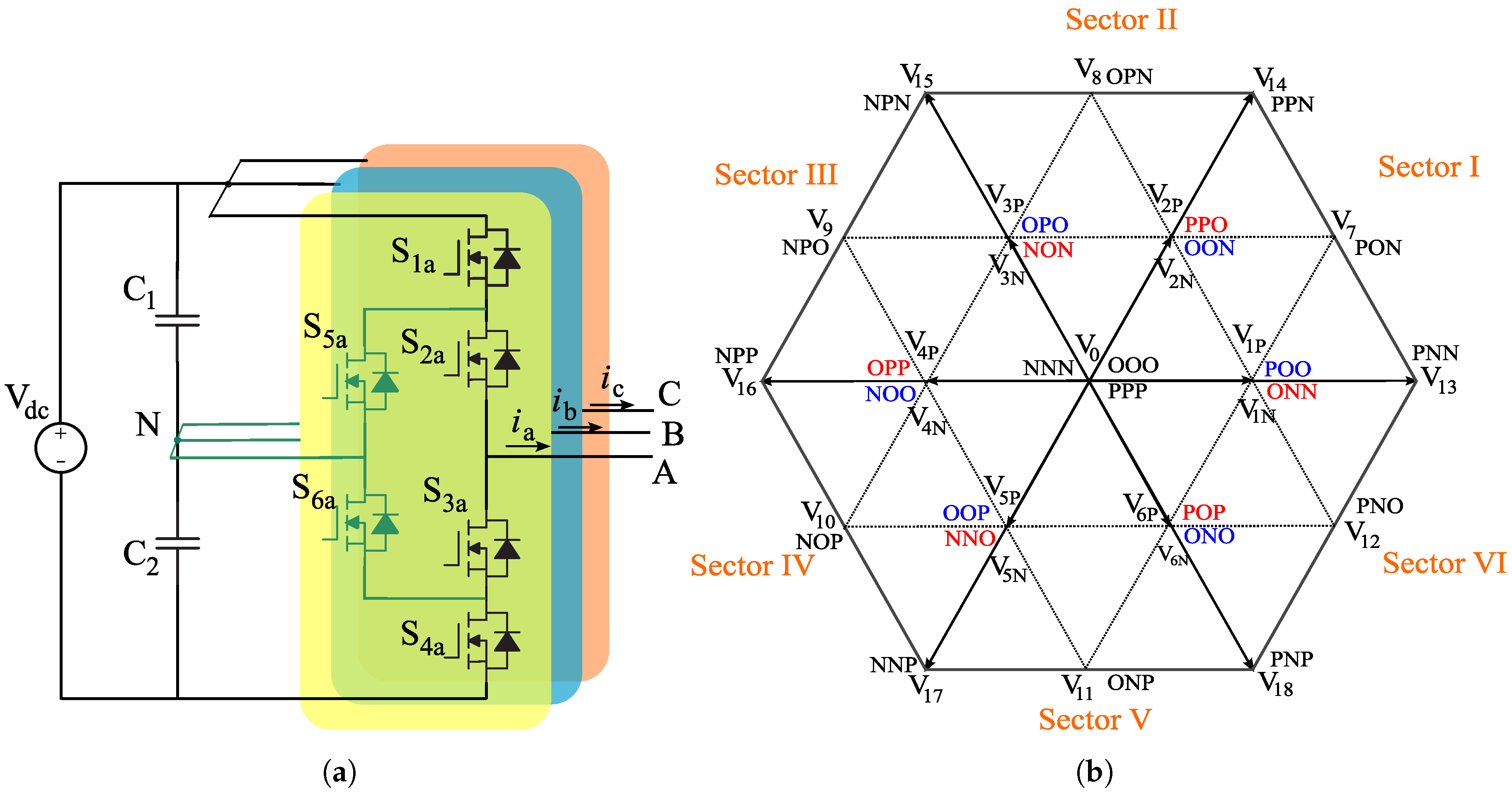
A three-level active neutral-point clamped (ANPC) inverter is shown in Figure 1a. In comparison with the NPC inverter, the diodes are replaced with two fully controlled switches, and . This feature can be used to evenly distribute the power loss among the switching devices. Note that the space vector diagram remains the same as depicted in Figure 1b. The corresponding switching states of phase A are listed in Table 1. The positive, negative, and zero switching states are represented by ‘P’, ‘N’, and ‘O’, respectively.
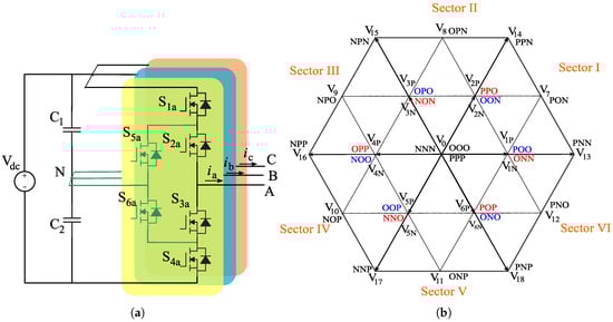
Figure 1.
(a) Topology of the ANPC and its (b) space vector diagram.

Table 1.
Switching states of a three-level ANPC.
2.1. Neutral-Point Current
Two DC-link capacitors, and , ideally have equal voltages (). The neutral-point voltage balance is essential for the decent performance of the ANPC. Each switching state affects the neutral-point voltage depending on whether a phase current flows through the NP or not. Large vectors contain no ‘O’ state, i.e., do not connect any phases to the NP. Therefore, they have no effect on the NPV. Likewise, zero vectors have no effect on the NPV. On the other hand, medium and small vectors each have a specific effect on the neutral-point current. Table 2 shows the neutral-point current for the medium and small vectors. It is assumed that the three-phase load is balanced:
Table 2.
The effect of medium and small vectors on the NP.
As an example, PON and NOP, both connect only phase B to the neutral point, therefore flows through the neutral. Similarly, POO connects phase B and phase C to the NP. Hence, the current flowing through the neutral would be .
In order to avoid the NPV fluctuations, one solution is to keep the average of the neutral-point current in one switching period at zero. It can be mathematically described as:
where denotes the duty ratio of the zero state for phase x, and likewise, the duty ratio of the other states is represented by and . By comparing (1) and (2), one can conclude that as long as the zero state ratio of all phases are equal, the neutral-point current is kept at zero, such that:
2.2. Common-Mode Voltage
As discussed in Section 1, CMV induces CM current in the parasitic capacitors resulting in EMI emissions. Moreover, higher CMV leads to higher leakage current that may damage the bearings and the motor insulation. Therefore, the CMV needs to be analyzed and considered in the design stage.
Common-mode voltage in a three-level inverter is defined as:
Table 3 summarizes the generated CMV by different space vectors.
Table 3.
Generated CMV by different space vectors.
2.3. Virtual Vectors
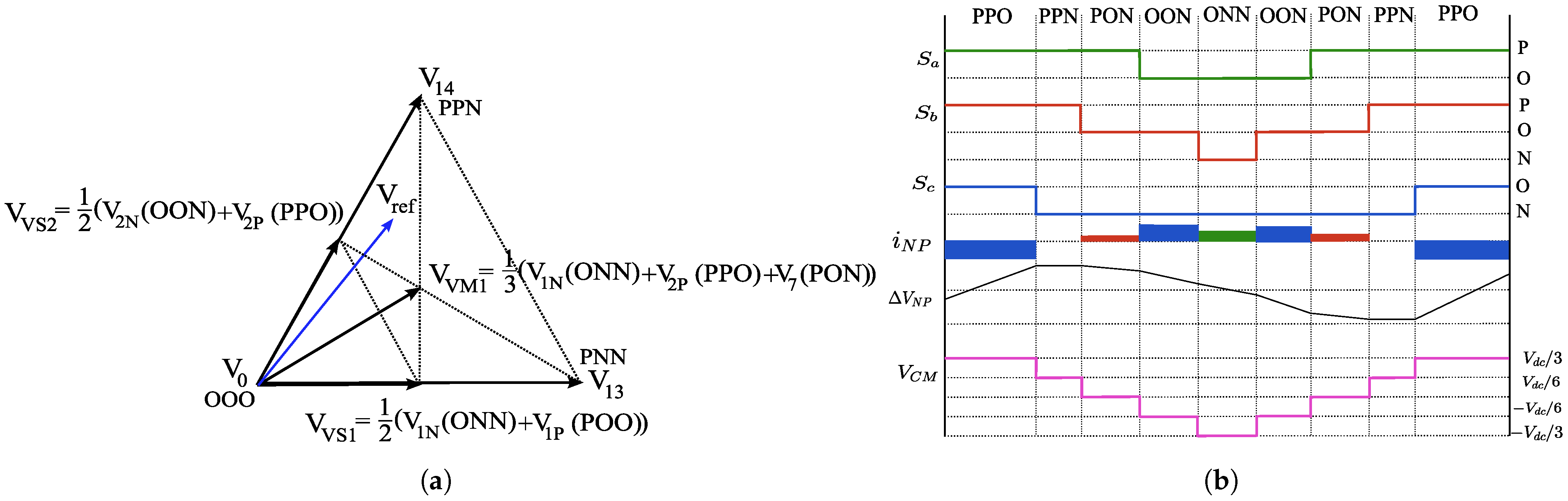
Virtual vectors are a linear combination of medium and small vectors that balance out their effect on the neutral-point current. In Figure 2a, the conventional virtual vectors in sector I are depicted [3]. In the new space vector diagram, large and zero vectors are the same as in the conventional SVD, while , , and are the new small (two) and medium virtual vectors. The small virtual vector is obtained by an equal combination of (POO) and (ONN). When is applied for a specific period of time, , each of the constitutive vectors, POO and ONN, are active for . The average neutral-point current can be calculated using Table 2:
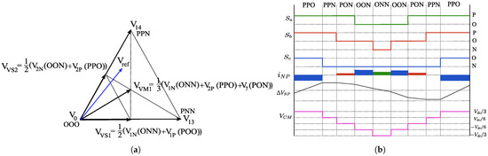
Figure 2.
(a) Virtual space vector diagram in sector I, (b) switching sequence of , resultant neutral-point current, NPV variations, and the generated . (Green: phase a; Red: phase b; Blue: phase c).
The average neutral point generated by the other small virtual vector, , is similarly zero. is an equal share of the medium space vector, (PON), and the small vectors (ONN) and (PPO). Notice that the generated neutral-point current of the constitutive vectors is , , and , respectively. Therefore, the resultant neutral current will be .
As an example, the switching sequence, the neutral-point current, and the neutral-point voltage deviations are graphically shown in Figure 2b for the reference voltage shown in Figure 2a. In this case, the nearest three virtual vectors are , , and . Hence, five different space vectors are applied: , , , , and . The switching sequences are arranged to minimize the switching power loss. Please note that it is assumed , , and .
The generated CMV of the sample switching sequence of the VSVPWM is depicted in Figure 2b. We can reduce the CMV to if only ‘OOO’ is used as a zero vector. In the same manner, CMV can be reduced to when the type 2 small vectors are eliminated. The CMV can be theoretically kept at zero by only using the medium vectors and zero state (’OOO’). However, this strategy is not applied in practical applications since we lose the major benefits of a three-level inverter.
In the new virtual space vector diagram, all the vectors have an average neutral-point current of zero. Although various versions of an SVD have been proposed in the literature, all of them are based on the concept of a zero average neutral-point current.
3. Derivation of the Proposed Hybrid CBPWM
Compared to SVPWM, carrier-based PWM is simpler to implement, especially for multilevel inverters where the number of available voltage vectors in the SVD increases considerably. A conventional CBPWM where two carrier waves are compared with the three-phase modulation waves is shown in Figure 3. Modulation waves can be written as:
where m and are the modulation index and the output fundamental frequency, respectively. The main disadvantage of this modulation is that there are large NPV deviations.
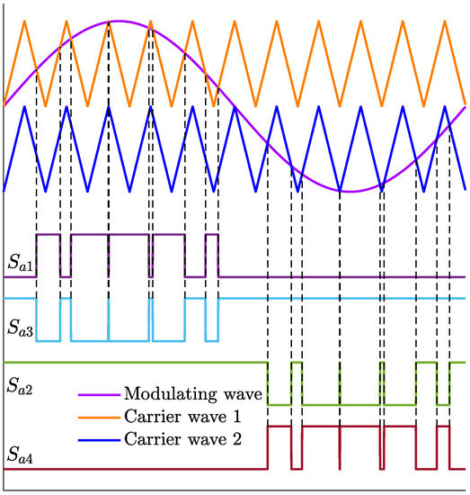
Figure 3.
Conventional CBPWM with two carriers.
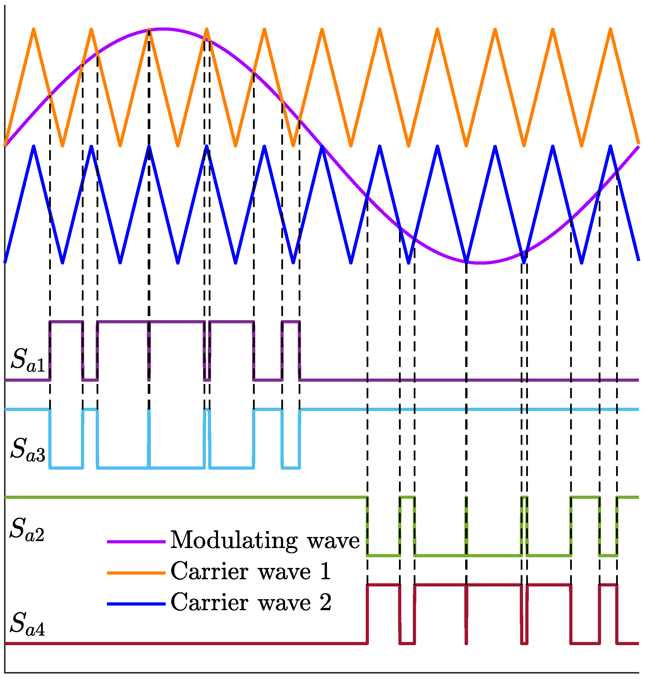
A double modulation CBPWM which includes the elimination of NPV fluctuations was first developed in [20]. This strategy is practically equivalent to the conventional VSVPWM studied in Section 2. Two modulation waves, known as positive and negative modulations, are compared with the carrier for each phase. The positive modulation wave () is used to control and and toggle the switching state of the phase leg between the ‘O’ and ‘P’ states. At the same time, the negative modulation wave is used to control and and toggle the switching state of the corresponding phase leg between the ‘N’ and ‘O’ states. The final switching state of the phase leg is obtained by combining the corresponding positive and negative switching states, as depicted in Figure 4.
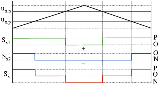
Figure 4.
Construction of the phase leg state using positive and negative modulation waves. (Green: negative modulation wave switching; Blue: positive modulation wave switching).
3.1. Principle of the Operation
The positive and negative modulation waves are obtained from the three phase modulation waves in (6). Based on [19], in order to derive the positive and negative modulation waves, the main reference voltages are rearranged as follows:
where is the maximum of the three modulation waves, is the minimum, and is the median modulation wave. Based on the volts-seconds product, the following can be written for the line voltages:
where are the switching states corresponding to ‘N’, ‘O’, ‘P’, respectively, and denotes the duty ratio of the state k and phase x. In other forms:
Since the sum of the duty ratios of the three states for each phase is equal to one, we also have the following:
The third equation in (9) can be achieved by adding up the first two. Therefore, in total there are five equations with nine unknowns in (9) and (10). Hence, more information is needed to solve the equations. First, we know that in order to achieve a zero average neutral-point current, the zero state ratio of all the phases should be the same, thus two more equations can be written as: ( = = ).
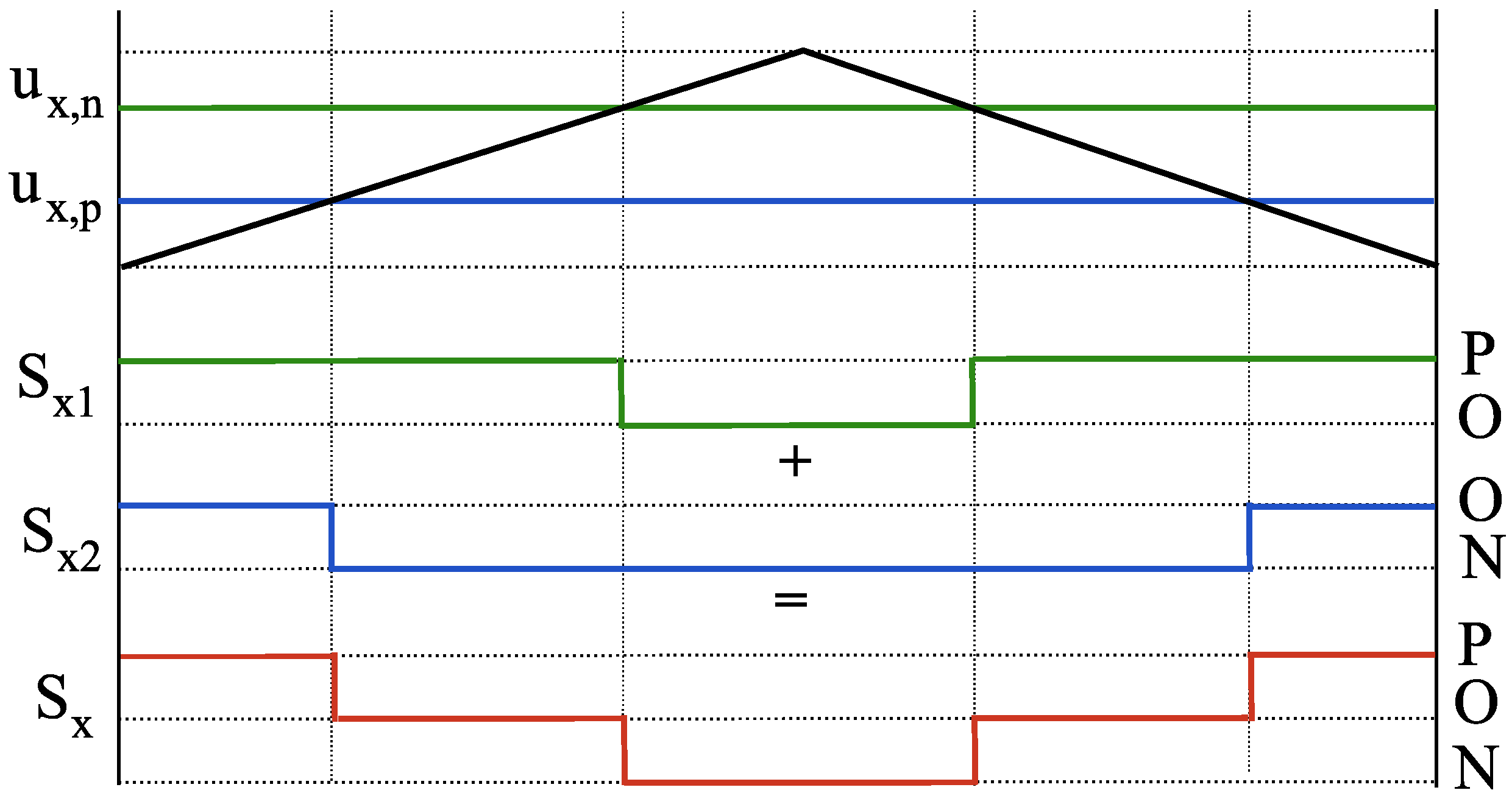
Two more restrictive conditions are required to uniquely solve the equations. Considering the space diagram (see Figure 1), in any Sector, the maximum voltage () switches between states ‘P’ and ‘O’. Similarly, the minimum voltage () only switches between ‘O’ and ‘N’, while the median voltage () is capable of all three states in every switching period. This can be seen for Sector I in Figure 2. In other words:
This limitation helps us to lower the switching power loss by reducing the total number of switching transients. It is worth mentioning that different restrictions can be applied to achieve other design objectives. The resultant duty ratios are obtained as follows:
Thus, in general, the modulation waves of phase x can be expressed as:
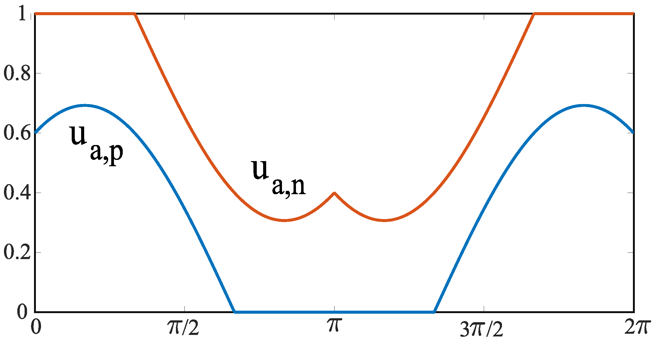
The positive and negative modulation waves for phase A, when , is shown in Figure 5.
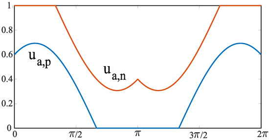
Figure 5.
Positive and negative modulation waves of phase A, .
3.2. CMV Reduction
The generated common voltage of the double modulation wave PWM is similar to the conventional VSVPWM shown in Figure 2, as long as the switching sequences are similar. The CMV can be reduced by rearranging the switching sequences. However, the calculated duty ratios in (13) must be satisfied in order to eliminate the NPV deviations.
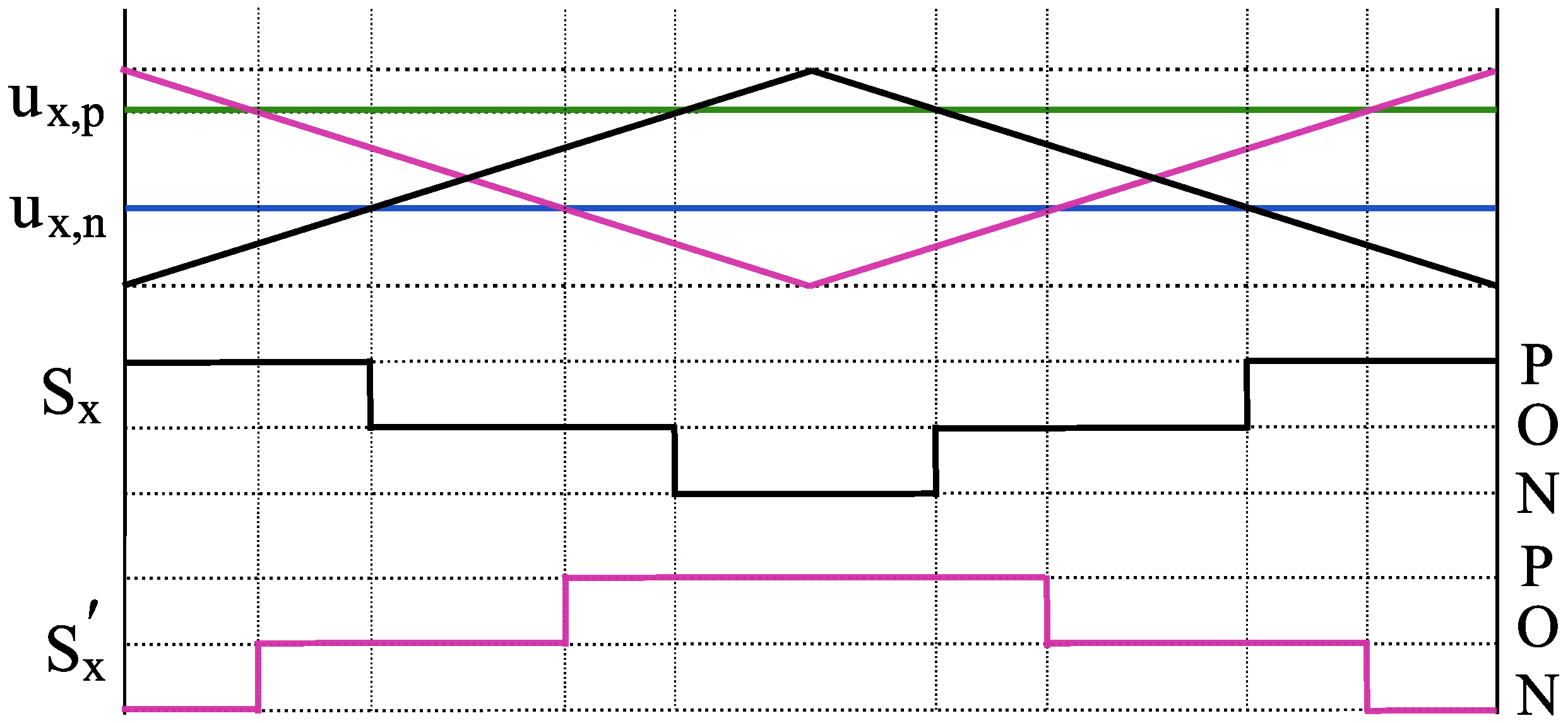
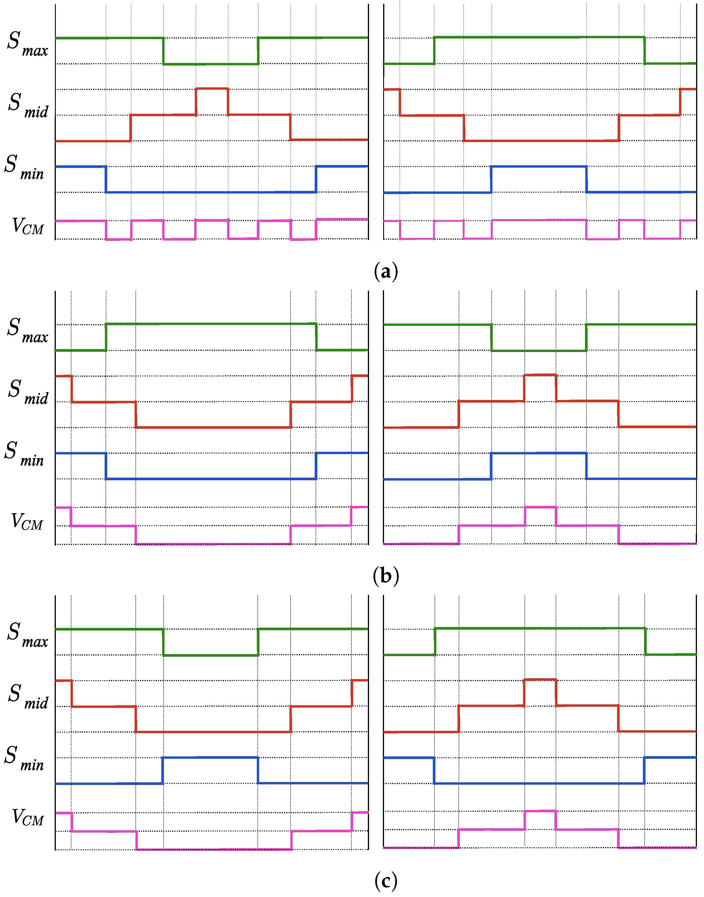
In Figure 4, each switching state follows the {high, low, high} pattern. The resultant switching state would be ‘PONOP’ for , ‘POP’ for , and ‘ONO’ for the . Another switching pattern is also possible when a carrier with opposite phase is implemented. As shown in Figure 6, with the {low, high, low} pattern, the resultant switching sequence, , is reversed in comparison with the previous case, , while the duty ratio of each state remains the same.
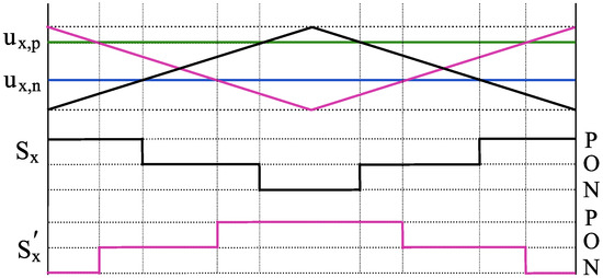
Figure 6.
Reversed switching patterns using two carriers with opposite phases.
In the case where only one of the carriers is used, the generated CMV can have an amplitude of up to . In order to eliminate the vectors with higher CMVs and limit their amplitudes to , both carriers should be used. With three phases and two carriers, six different combinations can be expected: two of the phases are compared to carrier wave 1 and the remaining phase is compared with carrier wave 2 (three combinations), or only one phase is compared with carrier wave 1 and the other two phases are compared with carrier wave 2 (three combinations). All six combinations are depicted in Figure 7 along with the generated in each case. Notice that all six cases have effectively reduced the CMV to as a result of using both carrier waves.
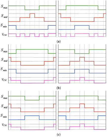
Figure 7.
Different combinations of switching sequences to reduce the CMV when the switching pattern is different for only (a) , (b) , and (c) , respectively.
Since each of the six possible combinations can ideally eliminate the NPV fluctuations and reduce the CMV, other aspects should be considered to compose the most efficient modulation scheme. In Figure 7, it is notable that the CMV has two levels when is reversed. On the other hand, the CMV changes between three levels when or are reversed. Therefore, the average CMV in one switching cycle is higher when is reversed. Higher average CMV results in higher leakage current leads to additional NPV deviations. In terms of the switching loss point, the sum of the switching transitions in one switching period is equivalent in all cases. Another factor is the harmonic content of the output voltage, which is studied next. It is worth mentioning that all three phases (a,b,c) should be reversed equally in a fundamental cycle in order to have balanced line-to-line voltages.
3.3. Harmonic Content
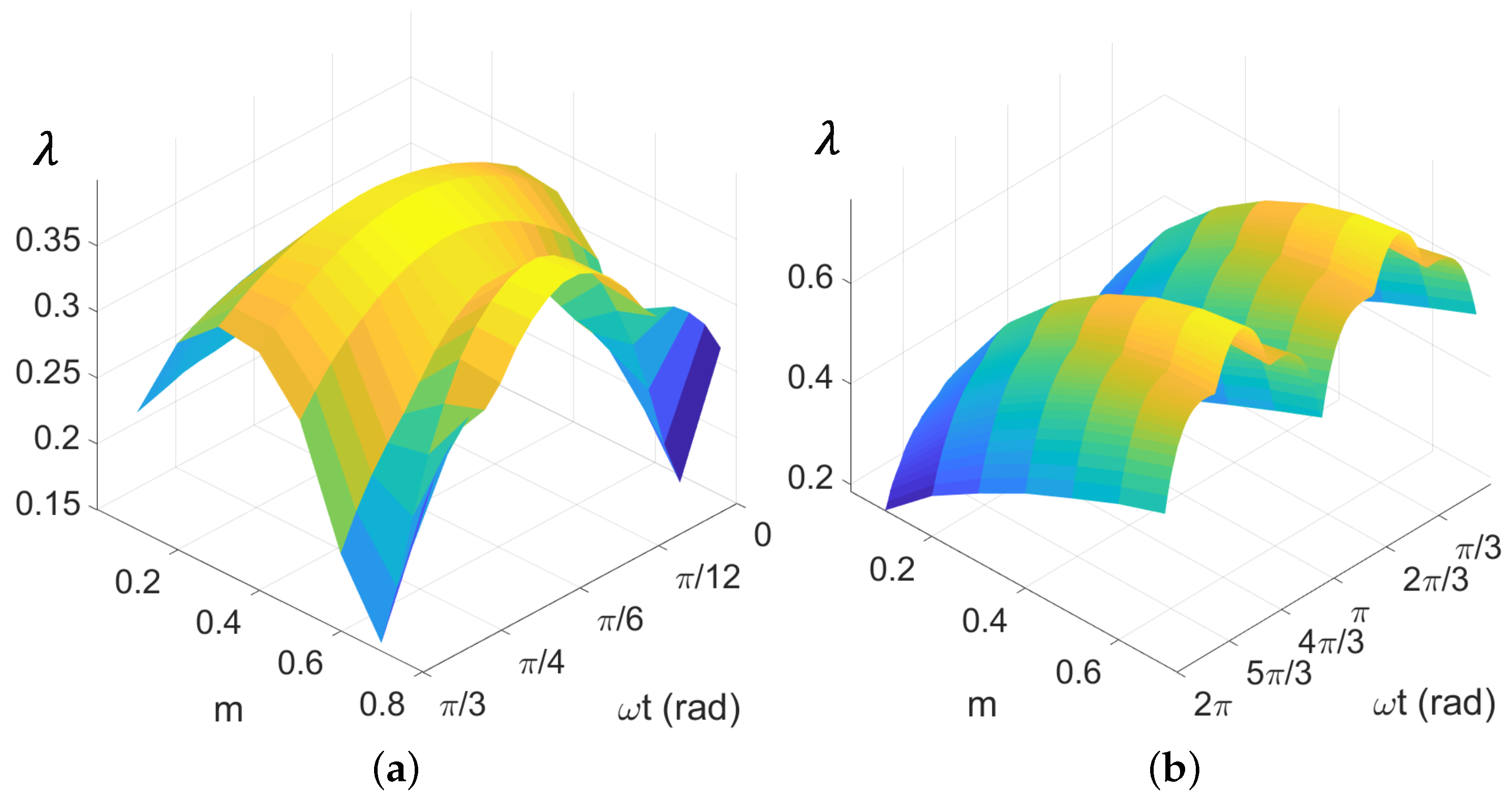
One of the most intuitive analytical approaches to evaluate the harmonic content is the harmonic flux trajectory (HFT), which uses the space vectors [21]. The harmonic flux in a switching period with a modulation index m is calculated as follows [22]:
where is the reference voltage vector with an angle of , and are the space vectors that are used to build the reference voltage. The RMS value of the flux in each switching cycle is a measure of the harmonic distortion and can be calculated as follows:
The HFT of the conventional CBPWM is shown in Figure 8a in Sector I for different modulation indices. In Figure 8b, the HFT of the RCMV-CBPWM is depicted with only reversed switching of . Contrary to the conventional CBPWM, it can be seen that the HFT of the second case does not follow the same pattern in all Sectors. Therefore, the RMS value of the HFT in a fundamental cycle, as calculated in (17), is used as a more intuitive parameter.
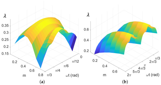
Figure 8.
Harmonic flux trajectories of (a) conventional CBPWM in Sector I, (b) double modulation RCMV-CBPWM when is reversed in all Sectors.
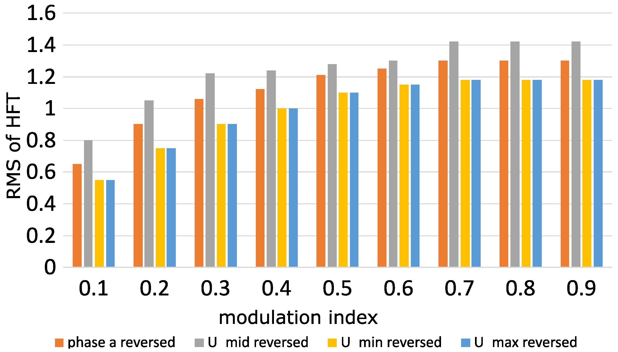
Four different reversed switching combinations are compared for different modulation indices in Figure 9: in one case, one phase is reversed at all times, and in the three other cases only one of the reference voltages (i.e., , , or ) is reversed at all times, which means all three phases are reversed equally in a fundamental cycle. It can be seen that the lowest harmonic content is achieved when either or is reversed.

Figure 9.
RMS value of the HFT in a fundamental cycle for four different reversed switching combinations.
3.4. Neutral Point Voltage Deviation
Thus far we have learned that the best results are achieved when either or is reversed, as shown in Figure 7b,c. Additional criteria are required to devise the best combination of reversed switching. Therefore, the variations of the neutral-point current are taken into account. Although the average of the neutral-point current in a switching cycle is equal to zero in all cases, the lower the RMS value the lower the NPV fluctuations within a switching cycle would be. The instantaneous neutral-point current is expressed as [23]:
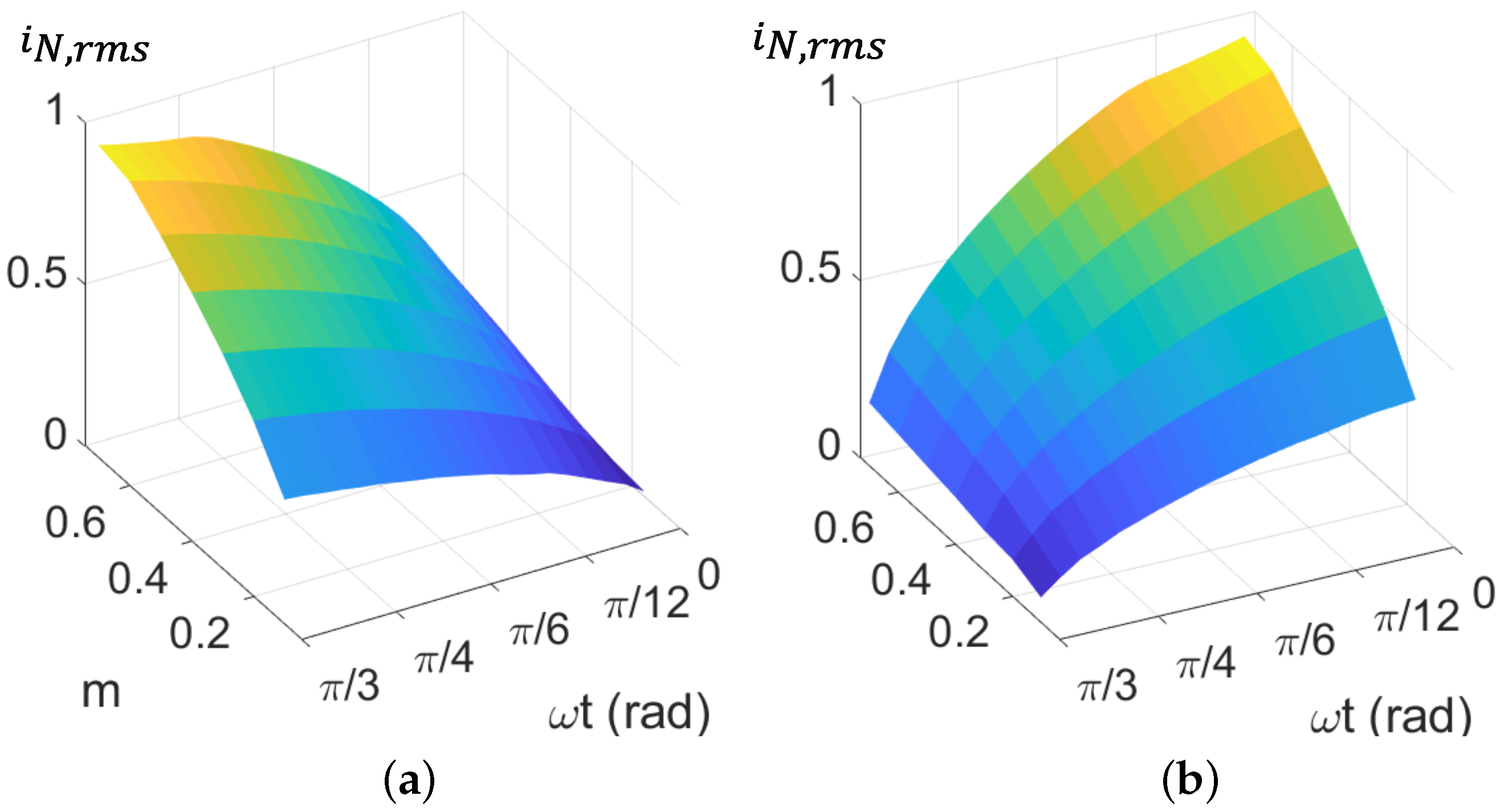
where is the switching state of phase x. The RMS value of the neutral-point current in each switching cycle is chosen as a performance criterion. For unity power factor, the neutral-point current deviation in the first Sector is shown in Figure 10 when either or is used at all times for the reversed switching. The asymmetric pattern of the neutral-point current is notable in both figures. It is assumed that the maximum output current is equal to one.

Figure 10.
Neutral-point current (rms) in the first Sector for unity power factor when (a) is reversed, (b) is reversed.
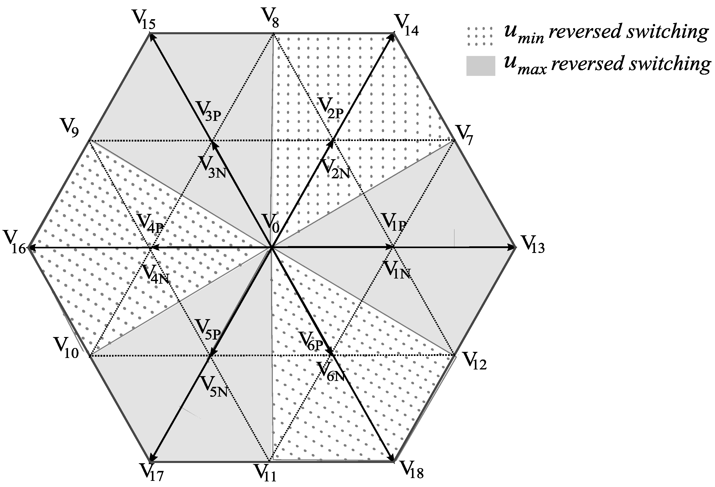
Based on the discussion above, in this paper, a new hybrid modulation is applied by combining the two mentioned cases, where both and are utilized for reversed switching. Using the SVD to divide each sector into two subsectors, in the first half of Sector I, is used for the reversed switching, while is used for the reverse switching in the second half. By using this strategy, the total neutral-point current variation is minimized. The resultant neutral-point current in the first Sector is depicted in Figure 11. The SVD of the proposed hybrid modulation is shown in Figure 12.
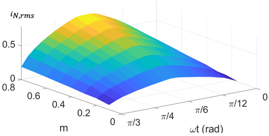
Figure 11.
Neutral-point current (rms) of the proposed hybrid modulation for unity power factor in the first Sector.
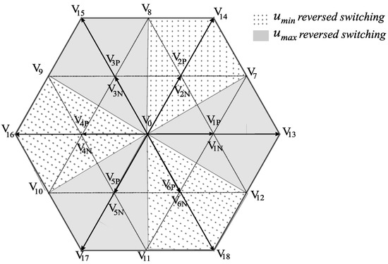
Figure 12.
Space vector diagram of the proposed hybrid CBPWM with reduced CMV.
4. Active NPV Controller
In ideal conditions, the average NPV is zero and the voltages of the DC-link capacitors are equal. However, in practice and would drift from due to various disturbances. Some of the influencing factors are the leakage current flowing through the ground wire and unequal DC-link capacitors. Therefore, an active controller is required to reduce the fluctuations of the neutral-point voltage.
The method proposed in [15] is used here for NPV balancing. since the neutral-point current is influenced by level 0 of each phase, the NPV deviations can be controlled by adjusting the level 0 of one or more phases. Notice that the line-to-line voltage should not be affected. In this paper, only the median phase is used for level 0 adjustment. The reason is that the line voltage can be kept the same since contains all three levels and hence there is no need to update the other phases.
In Figure 13, the adjustment of the duty ratio of is depicted. Assuming level 0 should be changed by , the duty ratio of level 1 and level −1 should likewise be updated since . In order to keep the line-to-line voltage the same, the voltage changes of should be zero:
where and are the DC-link capacitor voltages. Hence, duty ratio adjustment of different levels of can be calculated as follows:
.
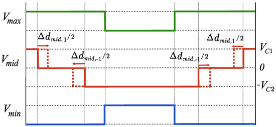
Figure 13.
Adjusting the duty ratio of the median phase, , for NPV control.
Figure 13.
Adjusting the duty ratio of the median phase, , for NPV control.
Assuming that the voltage difference between the DC-link capacitors is , the required compensating current for NPV adjustment is obtained by the following equation:
Because only is used for level 0 adjustment, the compensated current after adjustment is equal to . Therefore,
Thus, the duty ratio adjustments can be obtained from (22) and (20). It should be mentioned that the duty ratio adjustment is limited to the initial values. For example, when (the case shown in Figure 13), it is limited by and . This limitation can be mathematically expressed as:
When , it is limited by :
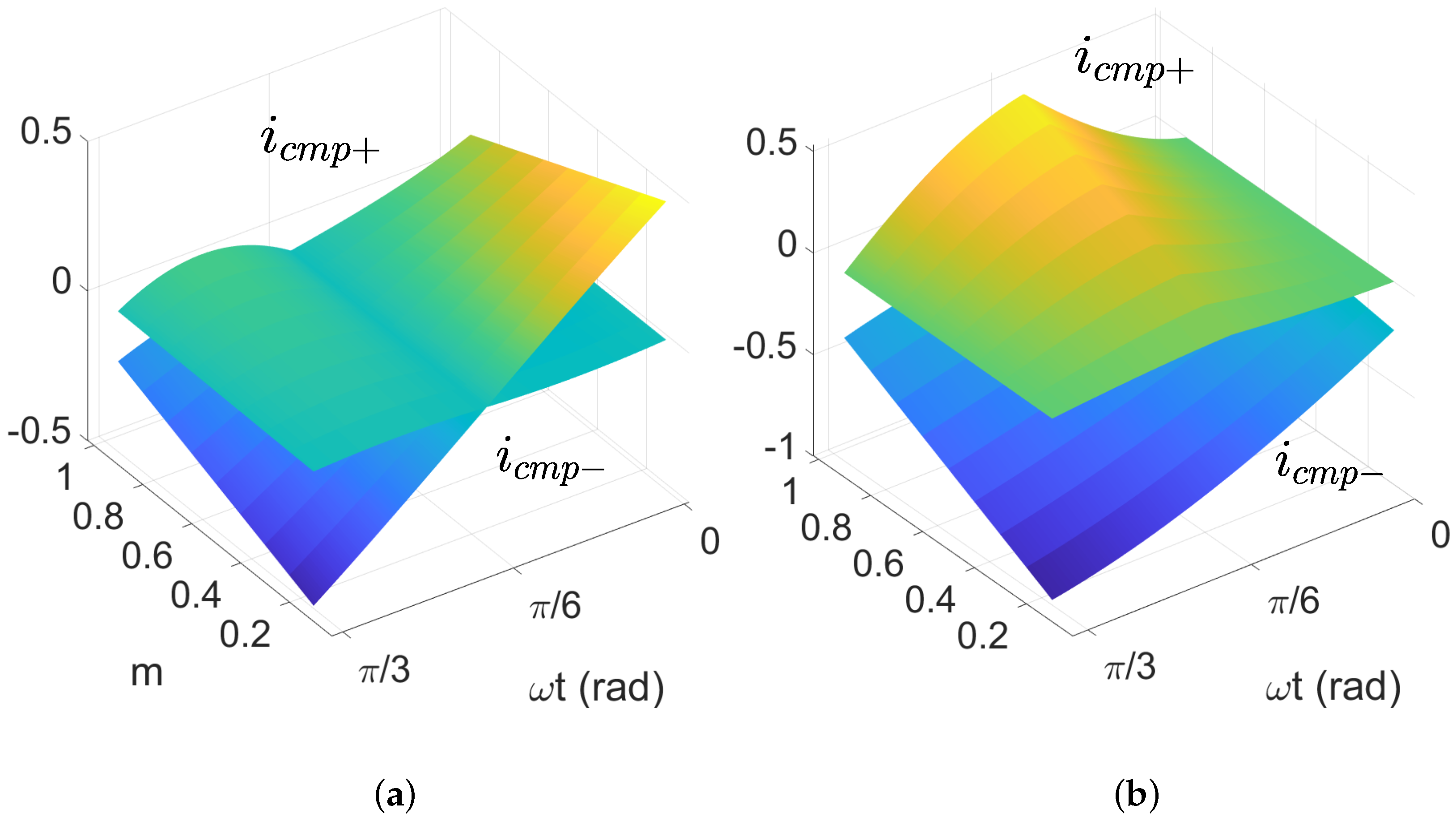
From (22), one can conclude that the compensating capacity is a function of the adjusted phase current, the DC-link capacitors, and the imbalance level of the capacitors. Furthermore, the compensating capability is not symmetric about zero according to (23) and (24). In Figure 14, positive and negative compensating currents are shown for different modulation indices and for two different power factors.

Figure 14.
Positive and negative compensating currents in Sector I when (a) , (b) .
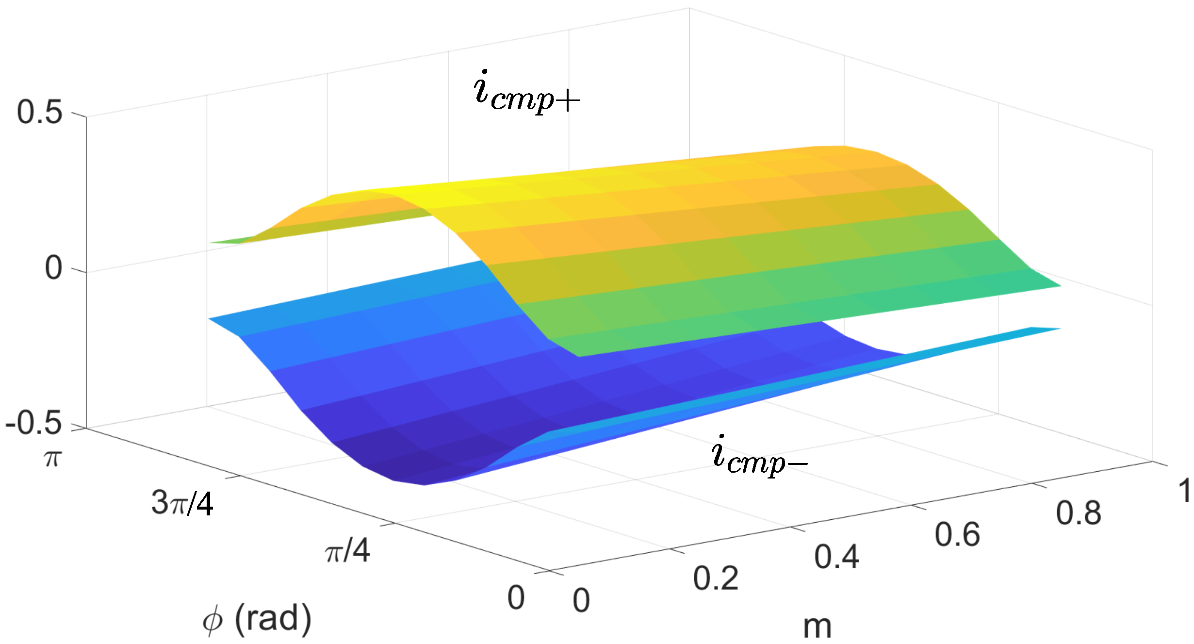
It is noticeable that the positive and negative compensating currents are not symmetric in Sector I. Therefore, the average current is calculated in a fundamental cycle using (25) and depicted in Figure 15 for various power factors and modulation indices. From Figure 15, one can conclude that the compensating current value is always non-zero, meaning that the controller is capable of balancing the neutral-point voltage in all operating conditions. However, the recovery speed is dependent on the power factor and modulation index. The controller can balance the NPV more quickly in low power factors and lower modulation indices.

Figure 15.
Average positive and negative compensating currents under different power factors and modulation indices.
5. Experimental Results
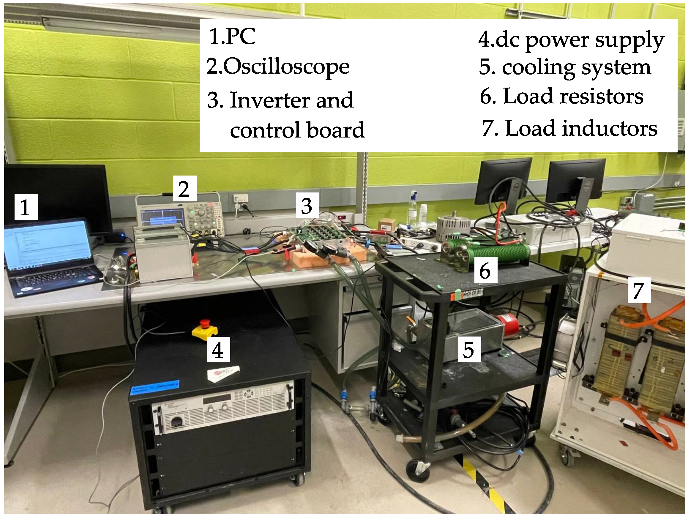
In this section, experimental results are presented to verify the performance of the proposed modulation. The experimental setup of the ANPC is shown in Figure 16 and the experimental parameters are listed in Table 4. Three modulation schemes are implemented in a TMS320f28379D microcontroller. The first case we examine is the conventional carrier-based modulation. The second case is the double modulation wave CBPWM with CMV reduction implemented in [19]. Lastly, the proposed hybrid CBPWM is applied to the inverter.

Figure 16.
The experimental setup of the 3-L ANPC.
Table 4.
Experimental parameters.
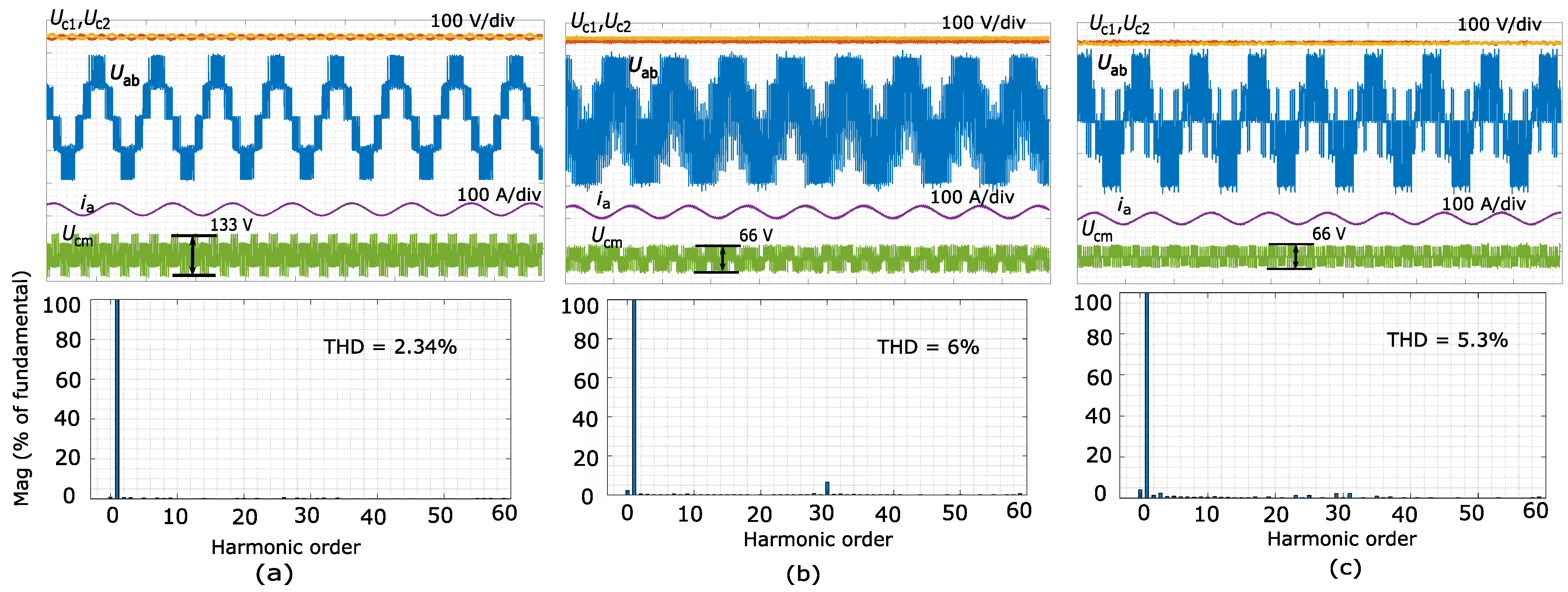
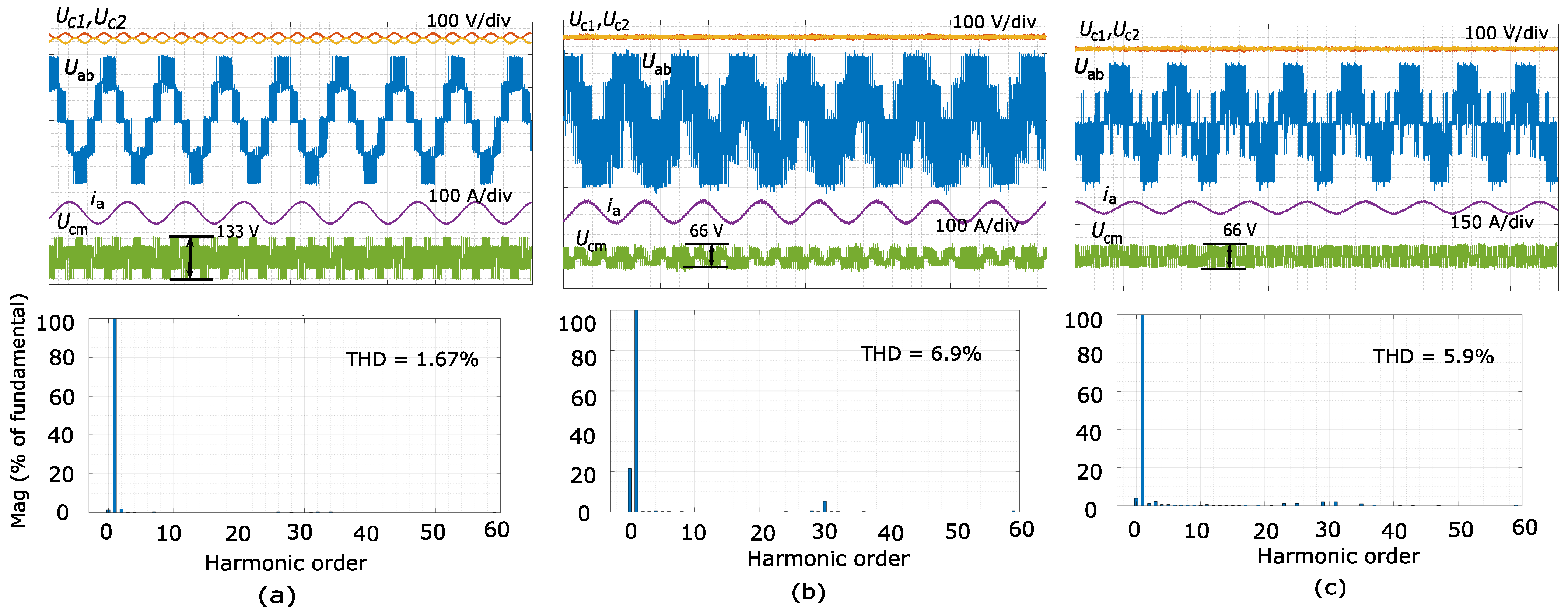
The experimental results are repeated for two cases: Case I considers using only an inductance load and a power factor () , whereas in Case II a series load is used and a power factor () . Measured line-to-line voltage, DC-link capacitor voltages, and generated common-mode voltages for all three modulations are shown in Figure 17 and Figure 18.
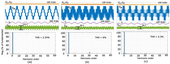
Figure 17.
Measured line-to-line voltage, DC-link capacitor voltages, output current , common-mode voltage , and harmonic content for Case I; (a) conventional CBPWM, (b) RCMV-CBPWM where only phase a is reversed, (c) proposed RCMV-CBPWM.

Figure 18.
Measured line-to-line voltage, DC-link capacitor voltages, output current , common-mode voltage , and harmonic content for Case II; (a) conventional CBPWM, (b) RCMV-CBPWM where only phase a is reversed, (c) proposed RCMV-CBPWM.
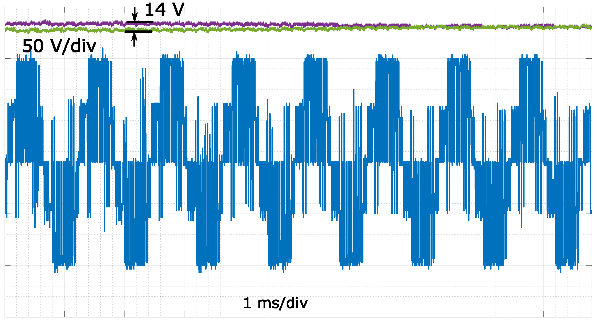
It can be seen that RMCV-CBPWM methods can suppress the CMV compared to the conventional CBPWM. The proposed method has lower harmonic content compared to the second method, however the conventional method results in the lowest harmonic. The main harmonics of the common-mode voltage are listed in Table 5 and Table 6, demonstrating that the proposed method produces the smallest harmonics. The performance of the active neutral-point controller is shown in Figure 19. A voltage perturbation is enforced to assess the NPV controller. The initial voltage error is 14 V and the controller recovers the voltage balance within 7 fundamental cycles.
Table 5.
Harmonic content of CMV for case I.
Table 6.
Harmonic content of CMV for case II.
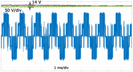
Figure 19.
Experimental results of voltage balancing control with the proposed method.
Conventional CBPWM provides the lowest THD at the expense of high common-mode voltage and NPV oscillations. In comparison with the available RCMV-CBPWM, the proposed modulation can effectively reduce the harmonic distortion, as well as the NPV oscillation. Furthermore, the generated CMV has lower harmonics.
6. Conclusions
In order to reduce the common-mode voltage and eliminate the neutral point oscillations in a three-level active NPC inverter, a new hybrid carrier-based PWM is proposed in this paper. This modulation is derived based on the theoretical analysis of the common-mode voltage and the neutral-point current ripples. Space vectors are selected to minimize the neutral-point current ripple. Furthermore, the proposed method limits the common-mode voltage and lowers the harmonics. A new space vector diagram is also provided.
Experimental results show that the proposed hybrid modulation effectively reduces the common-mode voltage and neutral-point voltage oscillations in comparison with the conventional CBPWM. This modulation is an improved RCMV-CBPWM that produces lower harmonic content and lower CMV harmonics.
Author Contributions
F.A.: Conceptualization, Investigation, Methodology, Writing—original draft; A.P.: Writing—review & editing, Visualization; A.E.: Supervision, Resources; B.B.: Supervision, Resources. Methodology, F.A.; Validation, F.A.; Resources, A.E.; Writing—original draft, F.A.; Writing—review & editing, A.P.; Visualization, A.P.; Supervision, A.E. and B.B.; Funding acquisition, B.B. All authors have read and agreed to the published version of the manuscript.
Funding
This research received no external funding.
Data Availability Statement
No new data were created or analyzed in this study. Data sharing is not applicable to this article.
Conflicts of Interest
The authors declare no conflict of interest.
References
- Wang, Y.; Poorfakhraei, A.; Mehdi, N.; Emadi, A. Comparative Analysis of 2-Level and 3-Level Voltage Source Inverters in Traction Applications. In Proceedings of the IEEE Transportation Electrification Conference Expo (ITEC), Chicago, IL, USA, 21–25 June 2021; pp. 614–619. [Google Scholar] [CrossRef]
- Kersten, A.; Oberdieck, K.; Gossmann, J.; Bubert, A.; Loewenherz, R.; Neubert, M.; Thiringer, T.; Doncker, R.W.D. Measuring and Separating Conducted Three-Wire Emissions From a Fault-Tolerant, NPC Propulsion Inverter With a Split-Battery Using Hardware Separators Based on HF Transformers. IEEE Trans. Power Electron. 2021, 36, 378–390. [Google Scholar] [CrossRef]
- Busquets-Monge, S.; Bordonau, J.; Boroyevich, D.; Somavilla, S. The nearest three virtual space vector PWM—A modulation for the comprehensive neutral-point balancing in the three-level NPC inverter. IEEE Power Electron. Lett. 2004, 2, 11–15. [Google Scholar] [CrossRef]
- Busquets-Monge, S.; Ortega, J.D.; Bordonau, J.; Beristain, J.A.; Rocabert, J. Closed-Loop Control of a Three-Phase Neutral-Point-Clamped Inverter Using an Optimized Virtual-Vector-Based Pulsewidth Modulation. IEEE Trans. Ind. Electron. 2008, 55, 2061–2071. [Google Scholar] [CrossRef]
- Busquets Monge, S.; Somavilla, S.; Bordonau, J.; Boroyevich, D. Capacitor Voltage Balance for the Neutral-Point- Clamped Converter using the Virtual Space Vector Concept With Optimized Spectral Performance. IEEE Trans. Power Electron. 2007, 22, 1128–1135. [Google Scholar] [CrossRef]
- Xiang, C.Q.; Shu, C.; Han, D.; Mao, B.K.; Wu, X.; Yu, T.J. Improved Virtual Space Vector Modulation for Three-Level Neutral-Point-Clamped Converter With Feedback of Neutral-Point Voltage. IEEE Trans. Power Electron. 2018, 33, 5452–5464. [Google Scholar] [CrossRef]
- Wu, X.; Tan, G.; Ye, Z.; Yao, G.; Liu, Z.; Liu, G. Virtual-Space-Vector PWM for a Three-Level Neutral-Point-Clamped Inverter with Unbalanced DC-Links. IEEE Trans. Power Electron. 2018, 33, 2630–2642. [Google Scholar] [CrossRef]
- Qin, C.; Li, X. Improved Virtual Space Vector Modulation Scheme for the Reduced Switch Count Three-Level Inverter with Unbalanced Neutral-Point Voltage Conditions. In Proceedings of the 2022 IEEE Energy Conversion Congress and Exposition (ECCE), Detroit, MI, USA, 9–13 October 2022; pp. 1–6. [Google Scholar] [CrossRef]
- Wang, J.; Gao, Y.; Jiang, W. A Carrier-Based Implementation of Virtual Space Vector Modulation for Neutral-Point-Clamped Three-Level Inverter. IEEE Trans. Ind. Electron. 2017, 64, 9580–9586. [Google Scholar] [CrossRef]
- Jiang, W.; Huang, X.; Wang, J.; Wang, J.; Li, J. A Carrier-Based PWM Strategy Providing Neutral-Point Voltage Oscillation Elimination for Multi-Phase Neutral Point Clamped 3-Level Inverter. IEEE Access 2019, 7, 124066–124076. [Google Scholar] [CrossRef]
- Weidong, J.; Wang, L.; Wang, J.; Zhang, X.; Wang, P. A Carrier-Based Virtual Space Vector Modulation With Active Neutral-Point Voltage Control for a Neutral-Point-Clamped Three-Level Inverter. IEEE Trans. Ind. Electron. 2018, 65, 8687–8696. [Google Scholar] [CrossRef]
- Hava, A.M.; Ün, E. A High-Performance PWM Algorithm for Common-Mode Voltage Reduction in Three-Phase Voltage Source Inverters. IEEE Trans. Power Electron. 2011, 26, 1998–2008. [Google Scholar] [CrossRef]
- Robles, E.; Fernandez, M.; Zaragoza, J.; Aretxabaleta, I.; De Alegria, I.M.; Andreu, J. Common-Mode Voltage Elimination in Multilevel Power Inverter-Based Motor Drive Applications. IEEE Access 2022, 10, 2117–2139. [Google Scholar] [CrossRef]
- Zhang, H.; Von Jouanne, A.; Dai, S.; Wallace, A.; Wang, F. Multilevel inverter modulation schemes to eliminate common-mode voltages. IEEE Trans. Ind. Appl. 2000, 36, 1645–1653. [Google Scholar] [CrossRef]
- Jiang, W.; Wang, P.; Ma, M.; Wang, J.; Li, J.; Li, L.; Chen, K. A Novel Virtual Space Vector Modulation With Reduced Common-Mode Voltage and Eliminated Neutral Point Voltage Oscillation for Neutral Point Clamped Three-Level Inverter. IEEE Trans. Ind. Electron. 2020, 67, 884–894. [Google Scholar] [CrossRef]
- Guo, F.; Yang, T.; Diab, A.M.; Yeoh, S.S.; Bozhko, S.; Wheeler, P. An Enhanced Virtual Space Vector Modulation Scheme of Three-Level NPC Converters for More-Electric-Aircraft Applications. IEEE Trans. Ind. Appl. 2021, 57, 5239–5251. [Google Scholar] [CrossRef]
- Xia, S.; Wu, X.; Zheng, J.; Li, X.; Wang, K. A Virtual Space Vector PWM With Active Neutral Point Voltage Control and Common Mode Voltage Suppression for Three-Level NPC Converters. IEEE Trans. Ind. Electron. 2021, 68, 11761–11771. [Google Scholar] [CrossRef]
- Hu, C.; Yu, X.; Holmes, D.G.; Shen, W.; Wang, Q.; Luo, F.; Liu, N. An Improved Virtual Space Vector Modulation Scheme for Three-Level Active Neutral-Point-Clamped Inverter. IEEE Trans. Power Electron. 2017, 32, 7419–7434. [Google Scholar] [CrossRef]
- Liu, P.; Duan, S.; Yao, C.; Chen, C. A Double Modulation Wave CBPWM Strategy Providing Neutral-Point Voltage Oscillation Elimination and CMV Reduction for Three-Level NPC Inverters. IEEE Trans. Ind. Electron. 2018, 65, 16–26. [Google Scholar] [CrossRef]
- Pou, J.; Zaragoza, J.; Rodriguez, P.; Ceballos, S.; Sala, V.M.; Burgos, R.P.; Boroyevich, D. Fast-Processing Modulation Strategy for the Neutral-Point-Clamped Converter With Total Elimination of Low-Frequency Voltage Oscillations in the Neutral Point. IEEE Trans. Ind. Electron. 2007, 54, 2288–2294. [Google Scholar] [CrossRef]
- Prieto, J.; Jones, M.; Barrero, F.; Levi, E.; Toral, S. Comparative Analysis of Discontinuous and Continuous PWM Techniques in VSI-Fed Five-Phase Induction Motor. IEEE Trans. Ind. Electron. 2011, 58, 5324–5335. [Google Scholar] [CrossRef]
- Glose, D.; Kennel, R. Continuous Space Vector Modulation for Symmetrical Six-Phase Drives. IEEE Trans. Power Electron. 2016, 31, 3837–3848. [Google Scholar] [CrossRef]
- Beniwal, N.; Townsend, C.D.; Farivar, G.G.; Pou, J.; Ceballos, S.; Tafti, H.D. Band-Limited Three-Level Modulation for Balancing Capacitor Voltages in Neutral-Point-Clamped Converters. IEEE Trans. Power Electron. 2020, 35, 9737–9752. [Google Scholar] [CrossRef]

Disclaimer/Publisher’s Note: The statements, opinions and data contained in all publications are solely those of the individual author(s) and contributor(s) and not of MDPI and/or the editor(s). MDPI and/or the editor(s) disclaim responsibility for any injury to people or property resulting from any ideas, methods, instructions or products referred to in the content. |
© 2023 by the authors. Licensee MDPI, Basel, Switzerland. This article is an open access article distributed under the terms and conditions of the Creative Commons Attribution (CC BY) license (https://creativecommons.org/licenses/by/4.0/).