Abstract
High-voltage GaN switches can offer tremendous advantages over silicon counterparts for the development of high-efficiency switching-mode power converters at high commutation frequency. Nonetheless, GaN devices are prone to charge-trapping effects that can be particularly relevant in the early-stage development of new technologies. Charge-trapping mechanisms are responsible for the degradation of the dynamic ON-resistance () with respect to its static value: this degradation is typically dependent on the blocking voltage, the commutation frequency and temperature, and is responsible for the reduction of power converter efficiency. The characterization of this phenomenon is very valuable for the development of a new process to compare different technological solutions or for the final assessment of performance. This characterization cannot be made with traditional static or small signal measurements since degradation is triggered by application-like dynamic device excitations. In this paper, we propose a technique for the characterization of the dynamic of high-voltage GaN switches under real operating conditions: this technique is based on the design of a half bridge switching leg in which the DUT is operated under conditions that resemble its operation in a power converter. With this setup, the characterization of a 600 V GaN switch dynamic is performed as a function of variable blocking voltages and commutation frequency. Additionally, this technique allows the separation of thermal and trapping effects, enabling the characterization of the dynamic at different temperatures.
1. Introduction
High-voltage (i.e., >600 V) GaN power switches are today the major enabler toward the development of a new generation of switching-mode power converters with upgraded performance in terms of power density, efficiency and simplified thermal management. The superiority of this wide band gap (WBG) technology can be mainly summarized as reduced conduction and switching losses with respect to silicon technologies.
Compared to SiC WBG technology, for nominal breakdown voltages up to 650 V, GaN has also demonstrated the capability of further increasing the application frequency, allowing for an additional enhancement of volumetric power density, due to the reduced dimensions of magnetics and capacitors [1,2]. Higher-frequency regimes with associated high efficiency have also a beneficial impact in the choice converter topologies [3,4] and on the power converter control bandwidth. High-voltage GaN switches for power conversion applications are typically AlGaN/GaN-on-Si high electron-mobility transistors (HEMTs) ([5]). This type of device (mainly with SiC substrates) has a 20-year heritage in the field of RF and microwave applications, where it is nowadays adopted for the implementation of analog amplifiers delivering up to tens of watts up to 40–50 GHz. The adaptation of these technologies to power-converter applications required technological solutions to obtain higher breakdown voltages [6] (from tens of volts to several hundreds of volts) and the exploitation of p-doped GaN gate to get normally OFF devices [7] (RF/microwave GaN HEMTs are normally ON devices).
At present, these developments have led to the availability of GaN power switches with typical breakdown voltages up to 600–650 V and optimal driving voltage of about 5 V [8,9,10]. Other switches with 50 V, 100 V, 200 V breakdown voltage with very high current capability can also be found in the market [11,12], whereas only very few experimental devices of 900 V technologies have recently been proposed [13].
While there is a tremendous interest in this high-voltage GaN technology, especially in the automotive market [14], these products have a limited heritage, and several providers are still optimizing their processes internally or in contract research foundries. One peculiar characteristic of GaN technologies is the presence of charge-trapping effects. As documented in the literature, GaN transistors are always affected by trapping states that modulate the number of carriers available for conduction into the channel [15,16,17,18]. The high electric field induced by the high voltage applied to the device during the blocking state of switching-mode operation triggers charge capture. The charge trapping is a very fast process that is typically almost entirely activated even for a very short duration of the blocking voltage (ns). Conversely, when the device is driven into conduction with 0 V, the inverse phenomenon takes place, namely charge release [19], which is typically much slower. For this reason, operatively, when the blocking voltage is removed, and the device is switched ON for the conduction part of the period, several charges are not available for the conduction and the observed in dynamic condition is larger than its static value. The slower the charge release mechanism, the higher the degradation of dynamic [20,21]. The charge release time constants are accelerated by higher temperature. Thus, degradation is a function of the switching frequency (i.e., amount of time for charge release during the device ON time) and temperature. Moreover, it is also a function of the application voltage since the amount of charge trapping increases with the electric field, which is a function of the blocking voltage [22].
The dynamic modulation of is a very important topic since it directly affects the converter efficiency and can lead to reliability concerns due to the higher dissipated power than expected from nominal static characteristics of the device. While a complete elimination of this effect is impossible for GaN devices, its minimization is possible by means of technological choices and optimizations [23]. In this context, it is extremely useful for foundries and research centers to perform a reliable characterization of degradation in dynamic regime, in which the dependence of this phenomenon to voltage, frequency and temperature should be identified. Measurement set ups and procedures for this characterization are very challenging to develop, especially for the large-application voltages and very fast commutation dynamics of the technology. Several measurement techniques have been proposed in the literature [24,25,26,27,28,29,30], attesting to the importance of the topic. One of the targets of the measurement procedure must be the capability to test the DUT in a working regime as close as possible to the actual regime of the final application. Nonetheless, this is hardly achievable by the majority of the approaches proposed in the literature; hence, additional investigations are needed to precisely reproduce the application scenario during the device characterization. The proposed approach gives an additional contribution to the field of high-voltage GaN switches nonlinear dynamic characterization.
Toward this goal, in this paper, we propose a set-up and a measuring technique that accurately mimics the operating conditions of the real application. A custom switching module is designed in order to embed the DUT in a half-bridge switching-stage, and a measurement procedure is implemented to characterize its dynamic when operating as in a real power converter. The setup is designed to test 600–650 V switches in different voltage, frequency and temperature switching conditions. In Section 2, the measured procedure is described. The design and implementation of the switching module and of the measurement set up are described in Section 3 and Section 4, respectively. Finally, the results of the experimental characterization of 600 V GaN switches are provided in Section 5.
2. Measurement Procedure
The measurement procedure is similar to the one proposed in [31] for low voltage devices. The circuit described in this section implements a half-bridge commutation leg with two identical device samples. The low-side switch is the DUT, whereas the high-side device is used to complete the switching leg that is necessary to operate the DUT in the same condition of the real application. The working principle of the measurement technique is outlined in Figure 1a,b.
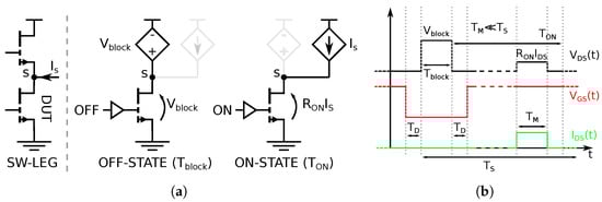
Figure 1.
Measurement technique working principle. (a) Switching leg states during the dynamic periodic measurement procedure; (b) waveforms of the proposed measurement technique.
When the switching leg is commutating, the period can be divided in two parts: during the DUT is OFF and the high side device connects the DUT drain to the blocking voltage (triggering charge trapping); during , the DUT is in conduction and a precise current source connected to the switching node S is used to inject a measuring current into the DUT. The measuring window within is called . During the measuring window, both the DUT current and the DUT voltage are sensed with accuracy so that the ON resistance is given by the ratio . According to Figure 1b a safety dead time is introduced between and transitions to avoid shoot through as in a real application. There are two ways to characterize the DUT dynamic as a function of the switching frequency, which are illustrated in Figure 2.
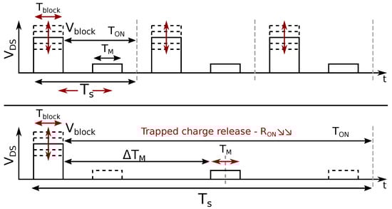
Figure 2.
Two different measurement regimes. Upper: direct characterization of varying the period . Lower: indirect characterization of at fixed period and varying .
The more direct method is to vary the period within the values of interests for practical applications and measure for every different switching frequency regime. The waveforms corresponding to this method are shown in the upper part of Figure 2: the drawback of this method is that the switching losses also vary with and so the different characterizations are not isothermal. This inhibits the possibility to separate trapping and thermal effects. As described in the lower trace of Figure 2, the alternative solution that we propose is to maintain a fixed, very long period with 99.9% duty cycle (i.e., and ) and characterize the variation over time by moving the measurement window along the very long of the DUT. Indeed, during , the trapped charge release mechanism takes place, decreasing the over time. This is an indirect, still equivalent, way to characterize the dependence of the dynamic vs. frequency since we can consider measured in equal to with . As can be observed in Figure 2, is the distance between the beginning of and of the associated trapped charge release mechanism, and the measuring instant. This consideration strictly holds if the duration of is not important for the observed device performance, which is an alternative way to state that the charge trapping event can be considered almost instantaneous, with respect to the application time scale. This has been verified and will be documented in the measurement section, and it was also observed in other studies [31]. With the proposed procedure, the characterization of the dynamic over time, and then, equivalently, over switching frequency, is isothermal, allowing to separate the thermal and trapping effects. Moreover, the DUT temperature can be known with fairly good precision by controlling the temperature of the testing module: indeed, by selecting values of the measuring current and measuring window small enough to have a negligible self-heating effect on the DUT, the DUT channel can be considered at the same temperature as the module carrier. Finally, the dependence of the dynamic on the application voltage can be assessed by varying the value applied to the DUT.
3. Design and Implementation of the Switching Module
As discussed in the introduction, the DUT is embedded in a switching module that accurately matches the actual operation of the DUT in a real application. Thus, the designed module is practically the active section of a half-bridge power converter. GaN technology characteristics set the specification for the module design. Here, the DUT is a 600 V p-GaN e-mode HEMT power device on silicon substrate of a process under development in a research foundry. In Table 1, the preliminary nominal electrical specifications of the switch are listed.

Table 1.
DUT electrical specifications.
The extremely low values of parasitic capacitances highlight the potentiality of this technology for very fast commutations. The expected commutation time is around 1 ns, which imposes to accurately design the power converter layout to minimize parasitic inductances and to select a proper driver and by-pass capacitors. As described in Figure 3, the DUT is in bare-die form with the gate, drain and source pads on the top of the die.
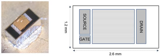
Figure 3.
Picture of the bare-die GaN power switch with some test wire bonding between source and drain pads and corresponding dimensions.
Therefore, all the connections to the rest of the module need to be provided with wire bonding, whose length must be kept as short as possible to minimize parasitics and have a minimal impact on commutation waveforms. Moreover, the die thickness of 1.05 mm further complicates the design of the switching module assembly (the die is not lapped to the typical 100 um thickness, since it comes from experimental wafers: this is very typical during process development). Thus, as illustrated in the sectional view of Figure 4, a double-board approach is followed.
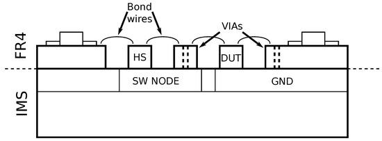
Figure 4.
Lateral section of half-bridge module.
A 2-layer 1 mm-thick FR4 board is dedicated to the placement of all the SMD components of the module, whereas the switches are placed at the same plane of the top of the FR4 board, exploiting two apertures implemented for their placement (see Figure 5). On the other hand, an IMS board is employed as a carrier of the GaN switches and stacked beneath the FR4 board. In this way, as can be appreciated in the photograph of Figure 5, the access points for the gate, source and drain pads are on the same level as the FR4 board, and the bonding wires’ length from the board to the die is minimized. The switches’ dies are attached to the IMS board by means of a high-thermal and high-conductive paste: the backside of the switches is the substrate potential, which must be connected to the source of each switch available in the upper side of the FR4 board, thanks to the wire bonding connections. Thus, as described in Figure 4, the filled VIAs in the FR4 board are used to connect the substrate potentials in the IMS board to the device sources on the top layer of the FR4 board.
Figure 5.
Photograph of the implemented half-bridge module with magnification of the die connections to FR4 board with wire bonding.
The FR4 board is populated with the SMD components, which are detailed in Figure 5. A high-side/low-side Si8273 isolated gate driver by Skyworks Solutions [32] is used to drive the GaN switches with = 0 V/+5 V. The component guarantees 2.5 k isolation, +1.8/−4 A forward/sink peak currents and very fast rise/fall times, which are ideal characteristics for GaN applications. The high-side driver configuration implements a diode-capacitor bootstrap circuit. The diode is a Schottky rectifier to reduce recovery time and withstand high blocking voltages [33], while is chosen as the bootstrap capacitance. It is noteworthy how the capacitance value could be selected to be ten times smaller for a typical design, given the very low gate charge of this device [34,35]; however, a bigger value was selected to sustain the high-side gate driving during the extended commutation periods used in the proposed characterization procedure described above. Two 1 W, 12 V–5 V low-ripple isolated DC/DC switching converters R1S-1205 by RECOM [36] were used to supply the first and second stages of the isolated gate driver. A 1 uF ceramic DC-link by-pass capacitor was placed close to the switching leg in parallel to the input voltage () to minimize the power loop stray inductance. The last component of the system is a PT100 thermistor directly placed on the IMS thanks to a third opening in the FR4 board. Even though the sensor is not very close to the switches, it provides a good temperature estimation, thanks to the wide aluminum substrate of IMS with high thermal conductivity.
4. Measurement Set-Up
As described in Section 2, the measurement of the dynamic implies the accurate sensing of the drain-source voltage and of the drain current during . As can be appreciated in Figure 5, the switching node of the half-bridge is easily accessible: at this node, the measuring current is injected, and is sensed, as described in the schematic of the set up in Figure 6a.
Figure 6.
Characterization set-up description. (a) Characterization set-up schematic; (b) photograph of the characterization set-up (IT6516C and isolated probe are not visible).
The measuring current is provided with a current source circuit already described in [31], made by two power Si P-MOS devices in cascode mode to maximize the generator output impedance. As described in [31], the current source is controlled with a ON/OFF command , while the current value is regulated by the value of the supply voltage . As observed before, it is important to regulate the amplitude and duration of the measuring current pulse in order to have a well-detectable , without inducing non-negligible self-heating to maintain isothermal conditions. The current value is measured by the Keysight high-bandwidth (100 MHz) Hall-effect probe N2783A with 1% accuracy. As described in Figure 6a, there are two different paths for the sensing of . One path with high dynamic range acquires the entire waveform along the period: in this path, an isolated active differential probe with 40 MHz bandwidth (Aaronia ADP1) is used to scale the waveform 100:1 to fit the oscilloscope voltage range. This channel is useful to monitor during and the synchronization with the measuring current, according to the measurement procedure described in Figure 1b and Figure 2, but this acquisition does not have enough sensitivity for a precise evaluation of during for the computation of . Thus, a second high-sensitivity and wide-band acquisition channel is implemented in a PCB visible in Figure 6b. In this channel, a low-offset and low-noise Analog Devices AD797 operational amplifier is used, in the ×20 voltage gain configuration described in the inset of Figure 6a. This acquisition channel enables the accurate characterization of waveforms during that are used for the computation of . Similar to that described in [31], with this configuration, the Op-Amp input is protected by means of two TVS diodes in anti-parallel configuration from high-voltage during . The presence of these didoes avoids the saturation of the oscilloscope acquisition channel and largely limits the saturation of the Op-Amp so that there are few s after the blocking event, and the Op-Amp exits saturation and is capable of correctly measuring . The high-resolution Tektronix MSO-56 scope is used for the time-domain acquisition of waveforms. The control of the power module and of the current generator according to the measurement procedure is provided by two synchronized arbitrary waveform generators (AWG): Agilent 81150A and Tektronix AFG320. The first AWG generates the PWM signals for the half-bridge switching module, while the second controls the current source.
5. Measurements
The measurement procedure described in Section 2 is adopted with the described setup. The duration of the blocking voltage is initially set to 1 us. The dead time is 500 ns. The value of the blocking voltage is varied between 10 V and 400 V. The duration of the measuring window is set to 40 s. The amplitude of the current injected by the controlled current source is set to 0.45 A, guaranteeing isothermal tests, since the induced temperature increment due to self heating is estimated in T = 0.22 C. This is also confirmed by the flat shape during the entire measuring window , which can be appreciated in the acquired waveforms (Figure 7 and Figure 8). The distance is varied from 20 s to 400 s that, according to the consideration in Section 2, corresponds to an equivalent switching frequency ranging from 50 kHz to 2.5 kHz. The acquired waveforms of the DUT , and for different blocking voltages are shown in Figure 7 for the acquisition at = 20 s and in Figure 8 for the acquisitions with = 400 s, respectively.
Figure 7.
and DUT waveforms acquired by the scope for = 20 s.
Figure 8.
and DUT waveforms acquired by the scope for = 400 s.
It can be observed that saturates the Op-Amp of the accurate acquisition channel of , but after less than 10 s, the Op-Amp exits saturation, and the measurement is available. The saturation of the Op-Amp and the presence of some residual ringing prevent the decrease of to lower values and thus directly observe for higher equivalent switching frequency. To this aim, the minimum can be reduced by a different selection of the Op-Amp. Nonetheless, observing the flat shapes of and pulses during suggests that negligible recovery is observed up to 60 s (i.e., + ) from the event. Therefore, it is safely possible to conclude that trap recovery is very slow and degradation is the same for application frequencies from 50 kHz upwards. This is an indirect, still reliable, indication that for this technology, the observed at 50 kHz is representative also for higher application frequencies.
From waveforms as the ones described in Figure 7 and Figure 8, = / is computed for different . The trends of the as a function of the blocking voltage evaluated at = 20 s, = 100 s and = 400 s are plotted in Figure 9, where the normalization factor is the value at = 0 V for all cases. The observed degradation of the dynamic is relevant.
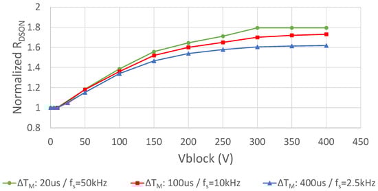
Figure 9.
Normalized dynamic VS evaluated at = 20 s, = 100 s and = 400 s, with a = 500 ns blocking voltage impulse.
It is useful to recall (as suggested in Figure 9) that the corresponding application frequencies are 50 kHz, 10 kHz and 2.5 kHz. Thus, since the target switching frequencies for high voltage GaN technology are typically in the range 50–500 kHz, the trap recovery does not give any beneficial effect to dynamic in the real application scenario. Therefore, the significant curve in Figure 9 is the one associated to = 20 s/ = 50 kHz (green curve), and for the consideration made before about the practical absence of recovery in the window = 20–60 s, this curve is the right reference also for higher switching frequencies. For this particular DUT, we can observe that the degradation of versus appears to saturate after 300 V. The explanation of this behavior is not immediate and should be investigated with a physic-level insight that is outside the scope of this paper.
The observed degradation is significant, with a maximum increase up to 80% with respect to the static value. This is quite typical for new GaN technologies under development, such as the one evaluated in this work, whereas more limited dynamic degradation can be observed for more mature commercial processes [18,29,30]. In this sense, the proposed technique can be a useful asset not only for the assessment of the performance of GaN transistor under operating regime, but also for the evaluation of the technological advances of a process under development.
Finally, Figure 10 describes the sensitivity of the dynamic to the duration of the blocking voltage . As expected, the effect is very limited and probably within the accuracy of the measurements. This corroborates the observation that the majority of charge-capture mechanisms are very fast.
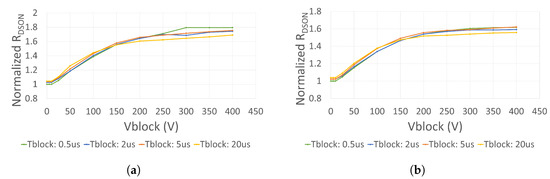
Figure 10.
Normalized VS evaluated in two distinct time instants . (a) at = 20 s for different ; (b) at = 400 s for different .
All the measurements were performed at DUT temperature (it is the temperature of the IMS, which corresponds to the DUT temperature since the measurement is isothermal with practically zero temperature increase). By varying the IMS temperature, the same characterization can be made to determine the variation of the degradation of dynamic vs. temperature. Unfortunately, these data are not available since we did not have a proper thermal controlled carrier capable to house the power module. When performing the same measurements at increasing IMS/DUT temperature, we expect a slight improvement of RON performance, as observed in [31] for lower voltage technologies. Finally, it is interesting to note that the proposed set up is also suitable to work in different regimes with respect to the one exploited for this characterization. Thus, other tests on the DUT dynamic can also be performed, forcing other conditions, such as hard/soft-switching, inductive load, double pulse, high-impedance, resonant-mode.
6. Conclusions
The Dynamic degradation of high-voltage GaN power transistors is a relevant topic that affects probably the most emerging semiconductor technology in the field of power electronics for automotive applications. The characterization of this phenomenon is a challenging research subject since it cannot be performed with standard techniques and instrumentation typically used for power transistor performance assessment. Indeed, static or small signal conductance measurement techniques cannot be applied, but unconventional non-linear dynamic approaches must be used. The main challenges associated with the set ups and measurement procedures are related to the need for a precise sensing of low-resistance values in the presence of fast commutations of high voltages.
Indeed, the most suitable method for the characterization of the dynamic of high-voltage GaN transistors is to measure this quantity during an operating regime of the DUT that resembles a real application scenario. For this reason, a measurement technique and a dedicated switching power module were developed and exploited for the characterization of bare-die 600 V GaN switches of a process under development. The measurements show a relevant degradation of that increases with the applied blocking voltage. This degradation fully applies to the entire range of switching frequencies of interests for this technology (i.e., >50 kHz). Indeed, due to the observed long time constants associated with trap-recovery mechanisms, a partial improvement of the dynamic is observed only for switching frequencies below 10–20 kHz, which are of very limited interest for this technology.
The proposed technique can be a useful method for the evaluation of high-voltage GaN switches’ dynamic during a real application scenario.
Author Contributions
Conceptualization, C.F., A.A. and A.S.; methodology, A.A., C.F.; software, A.A.; validation, A.A., C.F.; formal analysis, C.F., A.A.; investigation, A.A., C.F.; resources, C.F, A.S, E.S.; data curation, A.A.; writing—original draft preparation, A.A., C.F.; writing—review and editing, A.A., C.F., A.S., E.S.; visualization, A.A.; supervision, C.F., A.S., E.S.; project administration, C.F.; funding acquisition C.F., A.S., E.S. All authors have read and agreed to the published version of the manuscript.
Funding
This research received no external funding.
Data Availability Statement
The data presented in this study are available in the article
Conflicts of Interest
The authors declare no conflict of interest.
References
- Amano, H.; Baines, Y.; Beam, E.; Borga, M.; Bouchet, T.; Chalker, P.R.; Charles, M.; Chen, K.J.; Chowdhury, N.; Chu, R.; et al. The 2018 GaN power electronics roadmap. J. Phys. D Appl. Phys. 2018, 51, 163001. [Google Scholar] [CrossRef]
- Flack, T.; Pushpakaran, B.; Bayne, S. GaN Technology for Power Electronic Applications: A Review. J. Electron. Mater. 2016, 45, 2673–2682. [Google Scholar] [CrossRef]
- Ma, C.T.; Gu, Z.H. Review of GaN HEMT Applications in Power Converters over 500 W. Electronics 2019, 8, 1401. [Google Scholar] [CrossRef]
- Huang, Q.; Huang, A.Q. Review of GaN totem-pole bridgeless PFC. CPSS Trans. Power Electron. Appl. 2017, 2, 187–196. [Google Scholar] [CrossRef]
- Wang, H.; Wei, J.; Xie, R.; Liu, C.; Tang, G.; Chen, K.J. Maximizing the Performance of 650-V p-GaN Gate HEMTs: Dynamic RON Characterization and Circuit Design Considerations. IEEE Trans. Power Electron. 2017, 32, 5539–5549. [Google Scholar] [CrossRef]
- Kuzuhara, M.; Asubar, J.T.; Tokuda, H. AlGaN/GaN high-electron-mobility transistor technology for high-voltage and low-on-resistance operation. Jpn. J. Appl. Phys. 2016, 55, 070101. [Google Scholar] [CrossRef]
- Badawi, N.; Hilt, O.; Bahat-Treidel, E.; Böcker, J.; Würfl, J.; Dieckerhoff, S. Investigation of the Dynamic On-State Resistance of 600 V Normally-Off and Normally-On GaN HEMTs. IEEE Trans. Ind. Appl. 2016, 52, 4955–4964. [Google Scholar] [CrossRef]
- GaN Systems. 650V E-HEMT GaN TRANSISTORS; GaN Systems: Kanata, ON, Canada, 2023. [Google Scholar]
- STMicroelectronics. G-HEMT 650V GaN HEMT. 2023. Available online: https://www.st.com/en/power-transistors/g-hemt-650v-gan-hemt.html#overview (accessed on 25 January 2023).
- Instruments, T. Gallium nitride (GaN) ICs. 2023. Available online: https://www.ti.com/power-management/gallium-nitride/overview.html (accessed on 25 January 2023).
- Conversion, E.E.P. Product Selector Guide for Gallium Nitride (GaN) FETs and ICs. 2023. Available online: https://epc-co.com/epc/products/gan-fets-and-ics (accessed on 25 January 2023).
- GaN Systems. GaN TRANSISTORS 100 V E-HEMT; GaN Systems: Kanata, ON, Canada, 2023. [Google Scholar]
- Transphorm. Product Portfolio. 2023. Available online: https://www.transphormusa.com/en/products/ (accessed on 25 January 2023).
- Ding, X.; Zhou, Y.; Cheng, J. A review of gallium nitride power device and its applications in motor drive. CES Trans. Electr. Mach. Syst. 2019, 3, 54–64. [Google Scholar] [CrossRef]
- Meneghesso, G.; Meneghini, M.; Rossetto, I.; Bisi, D.; Stoffels, S.; Hove, M.V.; Decoutere, S.; Zanoni, E. Reliability and parasitic issues in GaN-based power HEMTs: A review. Semicond. Sci. Technol. 2016, 31, 093004. [Google Scholar] [CrossRef]
- Meneghesso, G.; Meneghini, M.; Chini, A.; Verzellesi, G.; Zanoni, E. Trapping and high field related issues in GaN power HEMTs. In Proceedings of the 2014 IEEE International Electron Devices Meeting, San Francisco, CA, USA, 15–17 December 2014; pp. 17.5.1–17.5.4. [Google Scholar] [CrossRef]
- Zulauf, G.; Guacci, M.; Kolar, J.W. Dynamic on-Resistance in GaN-on-Si HEMTs: Origins, Dependencies, and Future Characterization Frameworks. IEEE Trans. Power Electron. 2020, 35, 5581–5588. [Google Scholar] [CrossRef]
- Wang, W.; Liang, Y.; Zhang, M.; Lin, F.; Wen, F.; Wang, H. Mechanism Analysis of Dynamic On-State Resistance Degradation for a Commercial GaN HEMT Using Double Pulse Test. Electronics 2021, 10, 1202. [Google Scholar] [CrossRef]
- Cioni, M.; Zagni, N.; Iucolano, F.; Moschetti, M.; Verzellesi, G.; Chini, A. Partial Recovery of Dynamic RON Versus OFF-State Stress Voltage in p-GaN Gate AlGaN/GaN Power HEMTs. IEEE Trans. Electron Devices 2021, 68, 4862–4868. [Google Scholar] [CrossRef]
- Meneghesso, G.; Meneghini, M.; Silvestri, R.; Vanmeerbeek, P.; Moens, P.; Zanoni, E. High voltage trapping effects in GaN-based metal–insulator–semiconductor transistors. Jpn. J. Appl. Phys. 2015, 55, 01AD04. [Google Scholar] [CrossRef]
- Yang, S.; Han, S.; Sheng, K.; Chen, K.J. Dynamic On-Resistance in GaN Power Devices: Mechanisms, Characterizations, and Modeling. IEEE J. Emerg. Sel. Top. Power Electron. 2019, 7, 1425–1439. [Google Scholar] [CrossRef]
- Sun, S.; Xia, L.; Wu, W.; Jin, Y. Dynamic Ron Effect in GaN HEMT in a Zero-Voltage-Switching Circuit Due to Off-Resonance Operation. IEEE J. Electron Devices Soc. 2021, 9, 1155–1160. [Google Scholar] [CrossRef]
- Yang, S.; Zhou, C.; Han, S.; Wei, J.; Sheng, K.; Chen, K.J. Impact of Substrate Bias Polarity on Buffer-Related Current Collapse in AlGaN/GaN-on-Si Power Devices. IEEE Trans. Electron Devices 2017, 64, 5048–5056. [Google Scholar] [CrossRef]
- Modolo, N.; Meneghini, M.; Barbato, A.; Nardo, A.; De Santi, C.; Meneghesso, G.; Zanoni, E.; Sicre, S.; Prechtl, G.; Curatola, G. A novel on-wafer approach to test the stability of GaN-based devices in hard switching conditions: Study of hot-electron effects. Microelectron. Reliab. 2020, 114, 113830. [Google Scholar] [CrossRef]
- Meneghini, M.; Tajalli, A.; Moens, P.; Banerjee, A.; Zanoni, E.; Meneghesso, G. Trapping phenomena and degradation mechanisms in GaN-based power HEMTs. Mater. Sci. Semicond. Process. 2018, 78, 118–126. [Google Scholar] [CrossRef]
- Pirola, M.; Camarchia, V.; Quaglia, R.; Ramella, C. On-wafer characterization setup for model extraction and validation of high-power GaN HEMT switches. Int. J. Numer. Model. Electron. Netw. Devices Fields 2017, 30, e2118. [Google Scholar] [CrossRef]
- Subramani, N.K.; Sahoo, A.K.; Nallatamby, J.C.; Sommet, R.; Rolland, N.; Medjdoub, F.; Quéré, R. Characterization of Parasitic Resistances of AlN/GaN/AlGaN HEMTs Through TCAD-Based Device Simulations and On-Wafer Measurements. IEEE Trans. Microw. Theory Tech. 2016, 64, 1351–1358. [Google Scholar] [CrossRef]
- Badawi, N.; Dieckerhoff, S. A new Method for Dynamic Ron Extraction of GaN Power HEMTs. In Proceedings of the PCIM Europe 2015: International Exhibition and Conference for Power Electronics, Intelligent Motion, Renewable Energy and Energy Management, Nuremberg, Germany, 19–21 May 2015; pp. 1–6. [Google Scholar]
- Karboyan, S.; Uren, M.J.; Manikant; Pomeroy, J.W.; Kuball, M. Dynamic Ron in commercial GaN-on-Si HEMTs: HTRB stress and modelling. In Proceedings of the ROCS Workshop, Indian Wells, CA, USA, 22 May 2017. [Google Scholar]
- Foulkes, T.; Modeer, T.; Pilawa-Podgurski, R.N. Quantifying Dynamic On-State Resistance of GaN HEMTs for Power Converter Design via a Survey of Low and High Voltage Devices. IEEE J. Emerg. Sel. Top. Power Electron. 2020, 9, 4036–4049. [Google Scholar] [CrossRef]
- Cappello, T.; Santarelli, A.; Florian, C. Dynamic RON Characterization Technique for the Evaluation of Thermal and Off-State Voltage Stress of GaN Switches. IEEE Trans. Power Electron. 2018, 33, 3386–3398. [Google Scholar] [CrossRef]
- Skyworks. Si827x Datasheet. 2022. Available online: https://www.skyworksinc.com/-/media/Skyworks/SL/documents/public/data-sheets/Si827x.pdf (accessed on 25 January 2023).
- Vishay. VS-8EWS08STR-M3 Datasheet. 2019. Available online: https://datasheet.octopart.com/VS-8EWS08STR-M3-Vishay-datasheet-66898294.pdf (accessed on 25 January 2023).
- GaN Systems. How to Drive GaN Enhancement Mode HEMT; Technical Report GN001; GaN Systems: Kanata, ON, Canada, 2016. [Google Scholar]
- Skyworks Solutions. High-Side Bootstrap Design Using ISODrivers in Power Delivery Systems; Technical Report AN486; Skyworks Solutions: Irvine, CA, USA, 2021. [Google Scholar]
- Recom. R1S-R1D Datasheet. 2016. Available online: https://www.digikey.jp/ja/datasheets/recom-power/recom-power-r1s_r1d (accessed on 25 January 2023).
Disclaimer/Publisher’s Note: The statements, opinions and data contained in all publications are solely those of the individual author(s) and contributor(s) and not of MDPI and/or the editor(s). MDPI and/or the editor(s) disclaim responsibility for any injury to people or property resulting from any ideas, methods, instructions or products referred to in the content. |
© 2023 by the authors. Licensee MDPI, Basel, Switzerland. This article is an open access article distributed under the terms and conditions of the Creative Commons Attribution (CC BY) license (https://creativecommons.org/licenses/by/4.0/).