1. Introduction
Nowadays, industrial motor control systems are demanding high-precision and high-speed performance, which is mainly dependent on the encoder interface performance for transmitting motor position data [
1]. There are various encoder interface standards for industrial purposes, such as serial synchronous interface (SSI), HiperFace, EnDAT, and continuous bidirectional serial synchronous (BiSS-C) [
2]. Among them, the BiSS-C interface is supported by many prominent global motor companies, such as Paker, Maxon and Renishaw, and is expected to expand its market share in the future.
The BiSS-C interface is an open-source serial interface protocol that is similar to the SSI protocol, as the data transmission from an encoder is synchronized with the master clock signal based on the RS-422 standard. However, while the SSI transmission speed is limited to 2 Mbits/s, the maximum transmission speed of the BiSS-C interface amounts up to 10 Mbits/s. The SSI only supports unidirectional data transmission from slave to master; thus, no configuration data can be sent to the slave. However, since BiSS-C supports both unidirectional and bidirectional data transmission, the slave configuration can be controlled by the master in the BiSS-C interface. The BiSS-C protocol uses a cyclic redundancy check (CRC) for data verification, which is superior to the conventional parity check used by SSI [
3].
The configuration of BiSS-C communication can be classified into point-to-point and bus configurations. In a point-to-point configuration, only one BiSS-C slave device can be connected to the BiSS-C master device. In contrast, the bus configuration allows multiple slave devices to be connected to a single BiSS-C master device, and data from all slave devices are synchronized and collected to be sent to the master [
4,
5].
However, the BiSS-C encoders involve the following disadvantages in real applications. BiSS-C encoder specifications, such as the frame size and structure, are different for each encoder manufacturer. Hence, whenever the motor manufacturer is changed in a motor drive system, the BiSS-C interface master needs to be re-implemented to comply with the new BiSS-C encoder specification. In addition, the BiSS-C interface master needs to generate and control high-frequency clocks to receive high-speed slave encoder data, and the received high-speed data should be processed rapidly in the master. Implementing these master functions requires hardware logic circuits inevitably with high processing speed, which are usually implemented using field programmable gate array (FPGA) or complex programmable logic device (CPLD) [
6,
7]. This adoption of FPGA or CPLD causes the cost increase in production and maintenance because the number of integrated circuit (IC) parts, printed circuit board (PCB) size, artwork complexity, and power consumption increase accordingly.
As a way to solve these problems, Texas Instruments (TI) provides a BiSS-C interface library based on the logic design using a configurable logic block (CLB). However, it cannot be customized because its CLB design and internal C code are not open, which results in the limited usage of the BiSS-C interface library to certain specific microcontroller units (MCUs) and motor encoders only.
In this study, we develop a general method for designing and implementing a BiSS-C interface master for the point-to-point network configuration using only the CLB peripheral integrated into MCUs. By analyzing the detailed operation protocol of the BiSS-C interface, we create the truth and state tables for logic circuits and finite state machines, which are required for the BiSS-C interface master. Then, by programming the CLB based on the created truth and state tables, we implement the master clock, serial peripheral interface (SPI) clock, and operational process for the master.
Consequently, this approach using only the CLB is cost-efficient because FPGA- or CPLD-based additional hardware is unnecessary for the master implementation. That is, the production and maintenance costs are saved by reducing key factors, such as the number of IC parts, PCB size, artwork complexity, and power consumption [
8]. It is also beneficial that the developed method can be immediately applied to developing the masters for other types of BiSS-C encoders with different specifications, which is certainly necessary for a motor drive development and test. Moreover, the developed method can be used to improve the encoder data processing efficiency for the control and diagnostics of various industrial motor systems in automated factories [
9,
10].
To verify the performance and practical usefulness of the developed BiSS-C interface master, we build a motor control system consisting of the motor drive installed with the developed master and an AC motor with a BiSS-C encoder [
11,
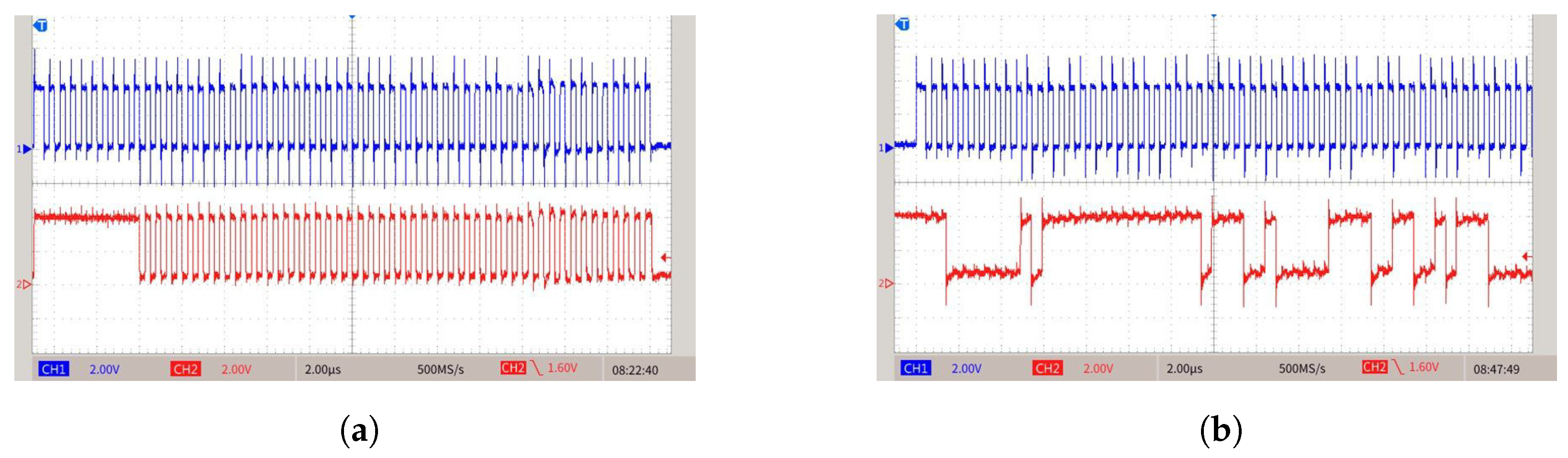
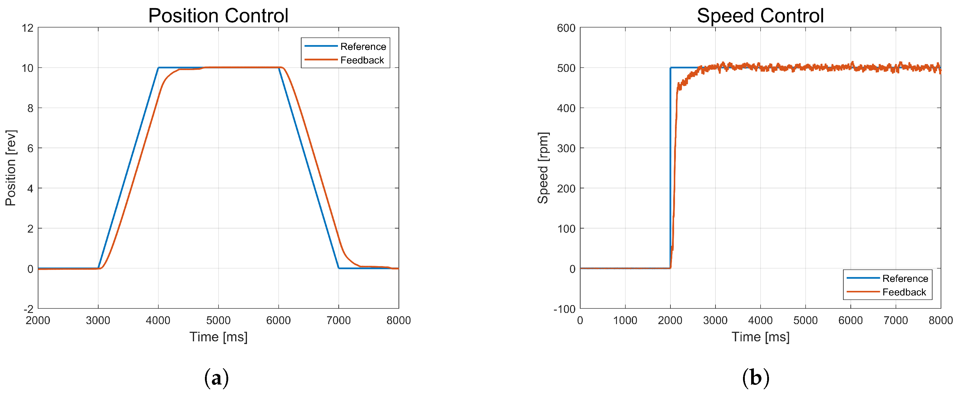
12]. We perform various experiments and verify the normal operation of the developed master by measuring the actual clock and data signals. The performance is verified by observing the normal operation with the MA frequency up to 6.25 MHz without any CRC errors. Moreover, the practical usefulness is demonstrated by showing the motor speed and position control performances that are acceptable in real applications.
The remainder of this paper is organized as follows. In
Section 2, the BiSS-C communication protocol and the CLB structure are explained. In
Section 3, the proposed BiSS-C interface is designed and implemented for the master. In
Section 4, an AC motor control setup is built, and various experiments are performed to verify the performance of the developed BiSS-C master interface. Finally, we present concluding remarks in
Section 5.
2. Relevant Background Knowledge
2.1. BiSS-C Protocol
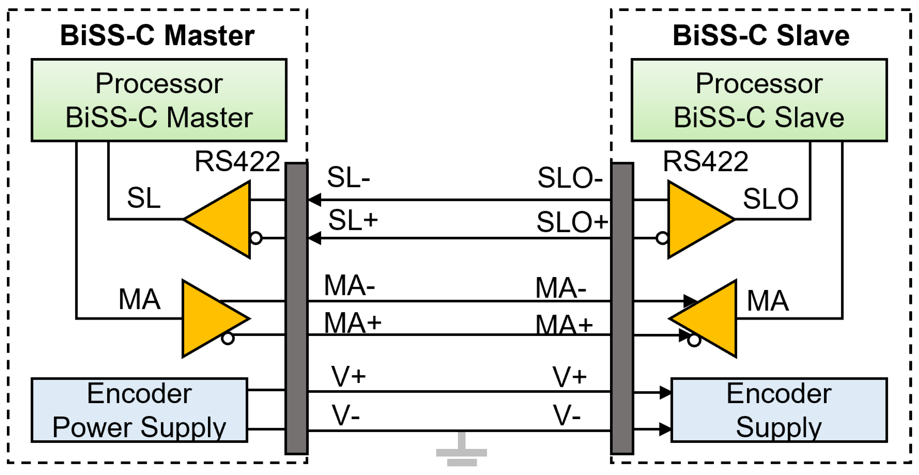
In a point-to-point configuration, a BiSS-C master device can be connected to a single slave device to which one or multiple sensors can be attached.
Figure 1 shows the hardware components in the point-to-point configuration. Among the six wires between the BiSS-C master and slave, the top four wires are assigned for MA+, MA−, SL+, and SL− in unidirectional full-duplex mode. MA and SLO denote the master clock and slave data signals, respectively. The remaining two wires are assigned for the encoder power supply, V+ and V−, where V− is typically grounded [
13].
In the BiSS-C communication protocol, the master provides its master clock to the slave, and then the slave sends data back to the master. The data frame from the BiSS-C slave includes the absolute position (single-turn), the total number of revolutions (multi-turn), temperature, parameters, and diagnosis data.
The BiSS-C communication data consist of single-cycle data (SCD) and control data (CD). SCD is the primary data transmitted from the slave to the master with sensor or actuator values and is updated every cycle. On the other hand, the CD enables the master to read and write the slave register as the master sends the control data master (CDM) bit to the slave, and the slave returns the control data slave (CDS) bit back to the master at each cycle. The parameters of a data channel, such as the CRC format and the number of frame bits, are specified by the slave and saved in an electronic data sheet (EDS).
As shown in
Figure 2, the MA signals request for the slave to send the BiSS-C frame, and the sent frame ends with the BiSS-C timeout state. In synchronization with the first rising edge of the MA, the slave activates data scanning and output, and at the second rising edge of the MA, the slave output (SLO) line changes to zero and generates an Ack signal. Then, the slave sends a CDS and a start bit and starts the actual data transmission. Note that the CDS bit of the encoder slave is almost zero because the master usually does not change the slave BiSS-C interface configuration in the case of encoder applications [
4,
7]. For the detailed operation protocol of bus configurations, it is recommended to refer to the BiSS interface protocol description in [
4].
2.2. CLB Structure and Functions
A CLB, functioning as a CPLD or FPGA, consists of programmable logic blocks and can be programmed to realize required logic circuits. The CLB is advantageous because it resides inside the TI MCU, allowing access to the central processing unit (CPU) or peripheral signals without pin delays.
Programmable logic and I/O Mux are provided in the CLB and can be configured by a CPU or control law accelerator (CLA) via configuration registers. The CLB can access input and output signals that reach inside the control peripherals, such as enhanced pulse width modulation (EPWM), quadrature encoder pulse (QEP), and enhanced capture (ECAP) peripherals. That is, the original input and output signals are not influenced by the CLB, but only internal signals can be changed and replaced by the CLB for completely newly customized peripherals, as shown in
Figure 3 [
8].
As shown in
Figure 4, a CLB consists of look-up tables (LUTs), counters, finite state machines (FSMs), output look-up tables (OUTLUTs), and a high-level controller (HLC), which are appropriately programmed and combined to realize a target logic system in the CLB design process [
14].
A LUT is composed of three or four inputs and one output, and the output can be designed as any form of combinational logic of inputs by controlling configuration registers. The HLC submodule provides the function to program instructions to process data between HLC general-purpose registers (GPREG) and selected registers in CLB submodules. The HLC programs are initially pre-loaded into the HLC instruction memory with the binary code generated in the CLB tool. The HLC instructions can be executed by triggering event signals, and the resources in the HLC can be written through data exchange registers by CPU or CLA.
As shown in
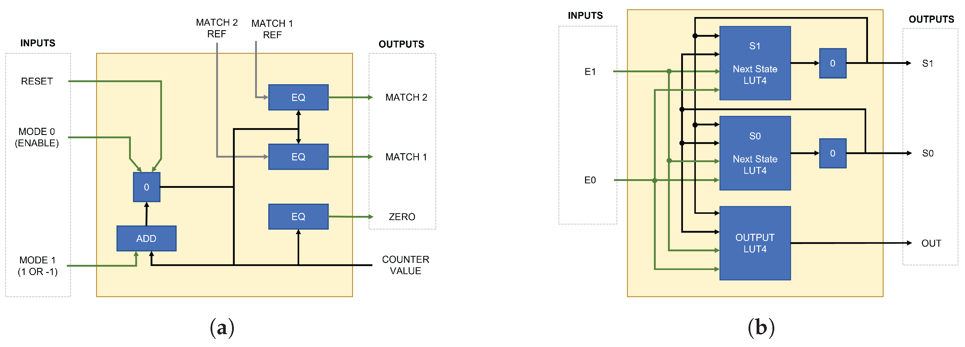
Figure 5a, the counter submodule has three inputs, four outputs, and two configuration parameters. Reset resets the counter value to zero, Mode 0 enables the counter, and Mode 1 determines up or down counting. MATCH1 and MATCH2 outputs generate a pulse signal when the counter values match MATCH1_REF and MATCH2_REF, respectively. The zero output generates a pulse when the counter is reset to zero value. As shown in
Figure 5b, an FSM consists of two inputs, E0 and E1, two state variable bits, S0 and S1, and one output, OUT. Inside the FSM, three LUT combinational blocks are available. Among them, two LUT blocks are used for the next state generation logic, and the last LUT block is used for the output generation logic.
The CLB integrated into the TI MCUs is configured and programmed using a software utility, CLB tool, which is included in the TI code composer studio integrated development environment (CCS IDE). Using the graphical user interface (GUI) options provided by CCS, the sub-modules of each CLB tile are configured and interconnected, and the logical equations for the LUTs and FSMs are programmed by text entry using C format. Then, the CLB tool generates a C header file containing a set of constants corresponding to the configuration settings defined by the user in the GUI. The tool also generates a C source file, which uses the constants in the C header file to initialize the CLB modules by loading the constants into the CLB registers by a sequence of register load operations. Finally, by compiling the generated source files and application files altogether, the binary execution file is created for the target MCU [
13].
3. Design and Implementation
In this section, we design and implement the motor encoder BiSS-C interface complying with the operation mechanism of the BiSS-C protocol based on the CLB peripheral. The operation process of the BiSS-C interface is described as follows:
- (i)
The interrupt service routine (ISR) of the EPWM device sends the encoder data request signal to the BiSS-C interface.
- (ii)
According to the encoder data request signal, the BiSS-C interface generates the MA signal and sends it to the encoder, namely, the BiSS-C slave.
- (iii)
In response to the MA signal, the encoder returns the SLO signal, that is, the position data.
- (iv)
The BiSS-C interface transfers the received position data to the motor control program, and one encoder data reading process is completed.
In the following subsections, we design each subsystem constituting the BiSS-C interface to realize the above operation process.
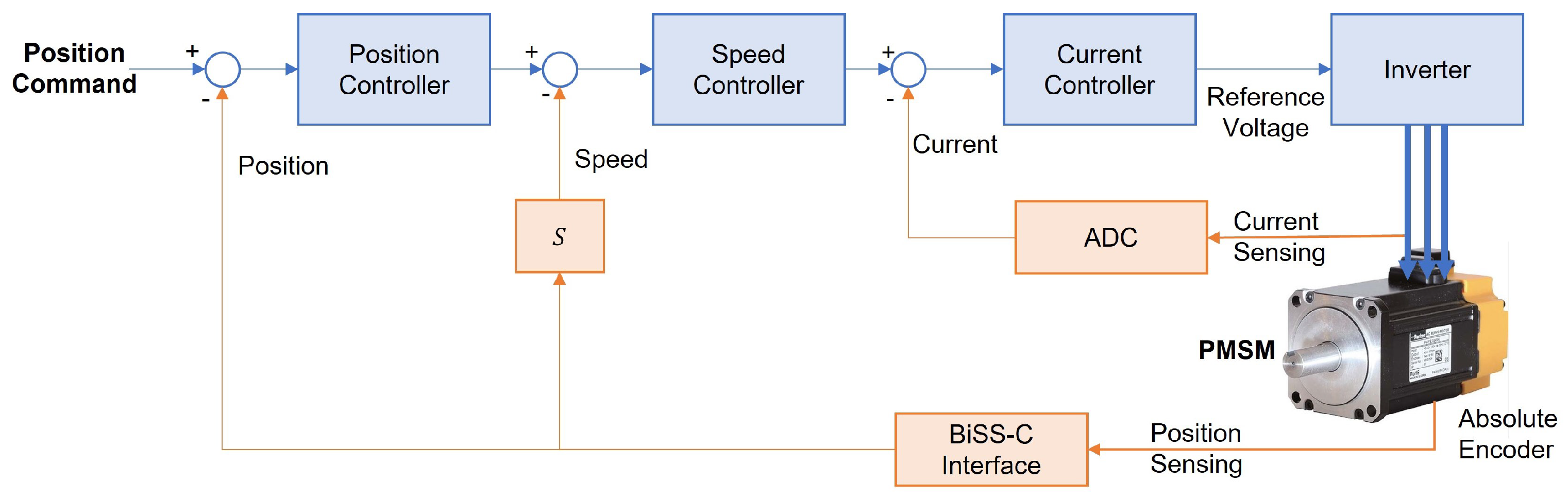
3.1. Hardware Structure
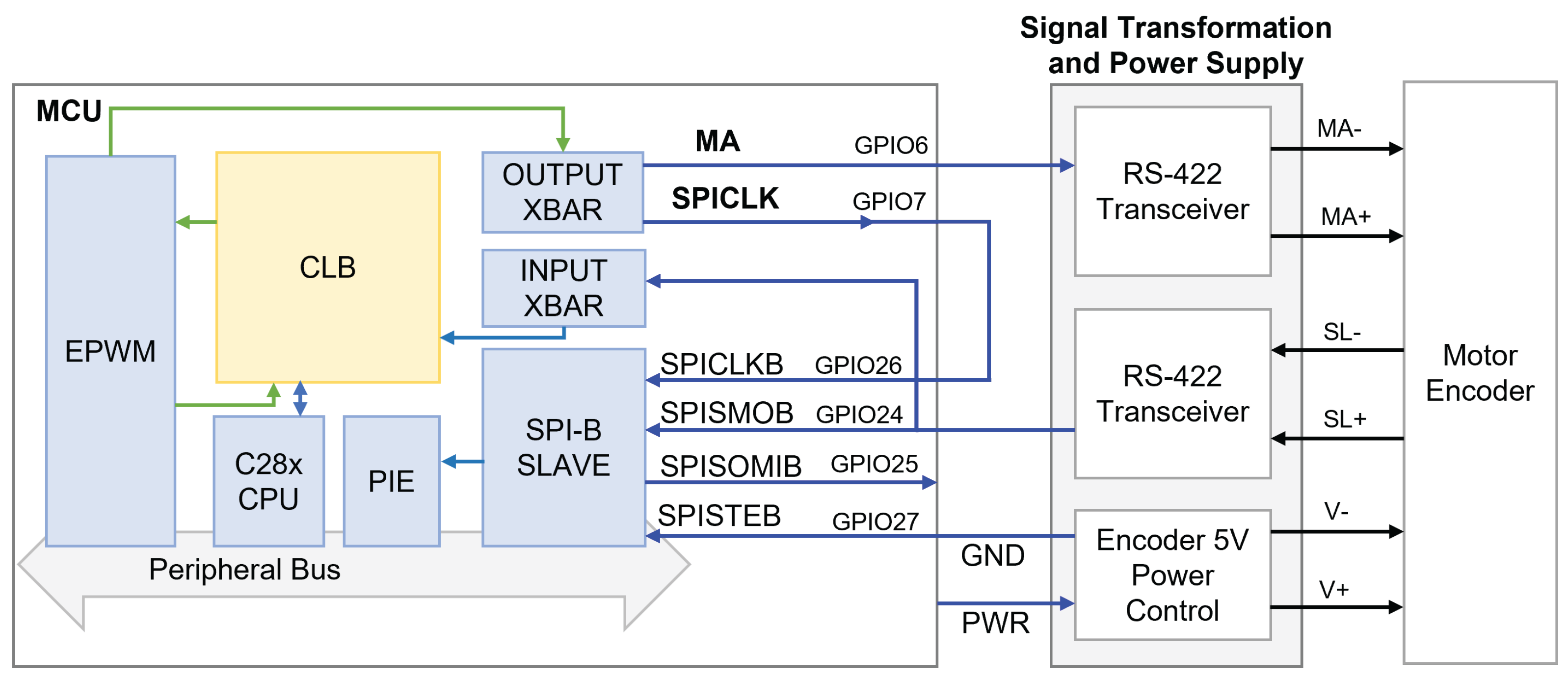
The BiSS-C communication requires the following hardware components: an MCU, a BiSS-C motor encoder, and a signal transceiver with a power supply, as shown in
Figure 6. The MCU works as a BiSS-C master device, while the motor encoder works as a BiSS-C slave device. Generally, the RS-422 communication device is used for the signal transceiver between the master and encoder.
The primary role of the BiSS-C master is to generate the master clock (MA) and SPI clock (SPICLK), read the data frame from the encoder, and convert them into position data. The main components of the MCU for the BiSS-C master implementation are a CPU, CLB, serial peripheral interface (SPI), and device interconnections (XBARs). The CPU is used to configure CLB data via the CPU bus, while the EPWM device is set up to be the outputs of CLB, which are the MA and SPICLK. XBARs and GPIOs are set up to export those clock signals and receive encoder data.
The MA is sent to GPIO6, and the SPICLK is sent to GPIO7 via OUTPUT XBAR. The MA from GPIO6 is converted into the differential signal, MA- and MA+ in the RS-422 transceiver, and finally sent to the motor encoder. Then, the motor encoder receives these MA+ and MA- clock signals and sends SL+ and SL- data signals back to the transceiver. Then, through the transceiver, the slave data signal is sent to the SPI-B SLAVE as the SLO data via GPIO24. The SPICLK is instantly generated at the first rising edge of SLO data and sent to the SPI-B SLAVE via GPIO7 [
15].
3.2. Clock Generation
Counters are key submodules used to generate clock signals. The counter structure is shown in
Figure 5a, and the basic operation principle is explained in
Section 2.2.
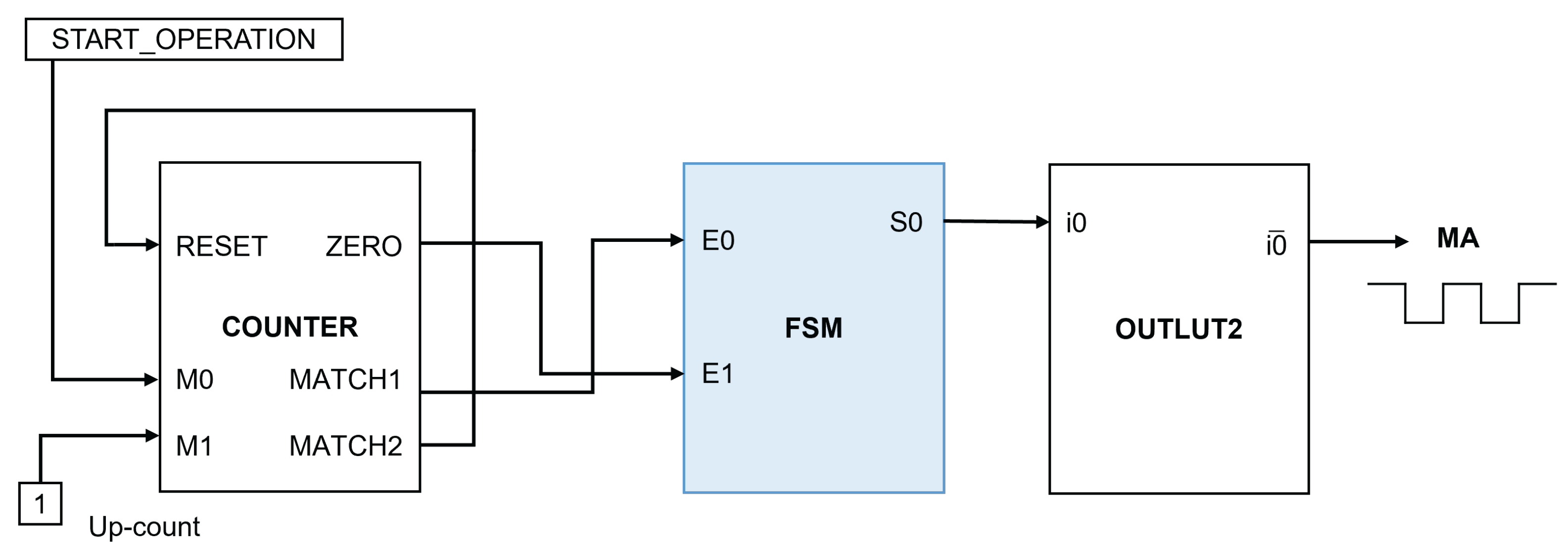
As shown in
Figure 7, using the counter outputs, ZERO and MATCH1 as FSM inputs and connecting the counter output, MATCH2, to the RESET counter input, a simple FSM can be easily designed such that the FSM generates a clock signal with the pulse width maintained between MATCH1 and MATCH2 output pulses. Based on the state diagram and state table shown in
Figure 8 and
Table 1, the next state equation and the output equation of the FSM is derived as
where
and
denote the current and next state of FSM; E0 and E1 denote the FSM inputs; and OUT denotes the FSM output. The structure and timing chart of this design are shown in
Figure 7 and
Figure 9, respectively.
In this design, the generated clock width and period are calculated as and , respectively. For example, when the system clock frequency is 100 MHz, the 2 MHz clock signal is synthesized by setting MATCH1_REF and MATCH2_REF values with 24 and 49.
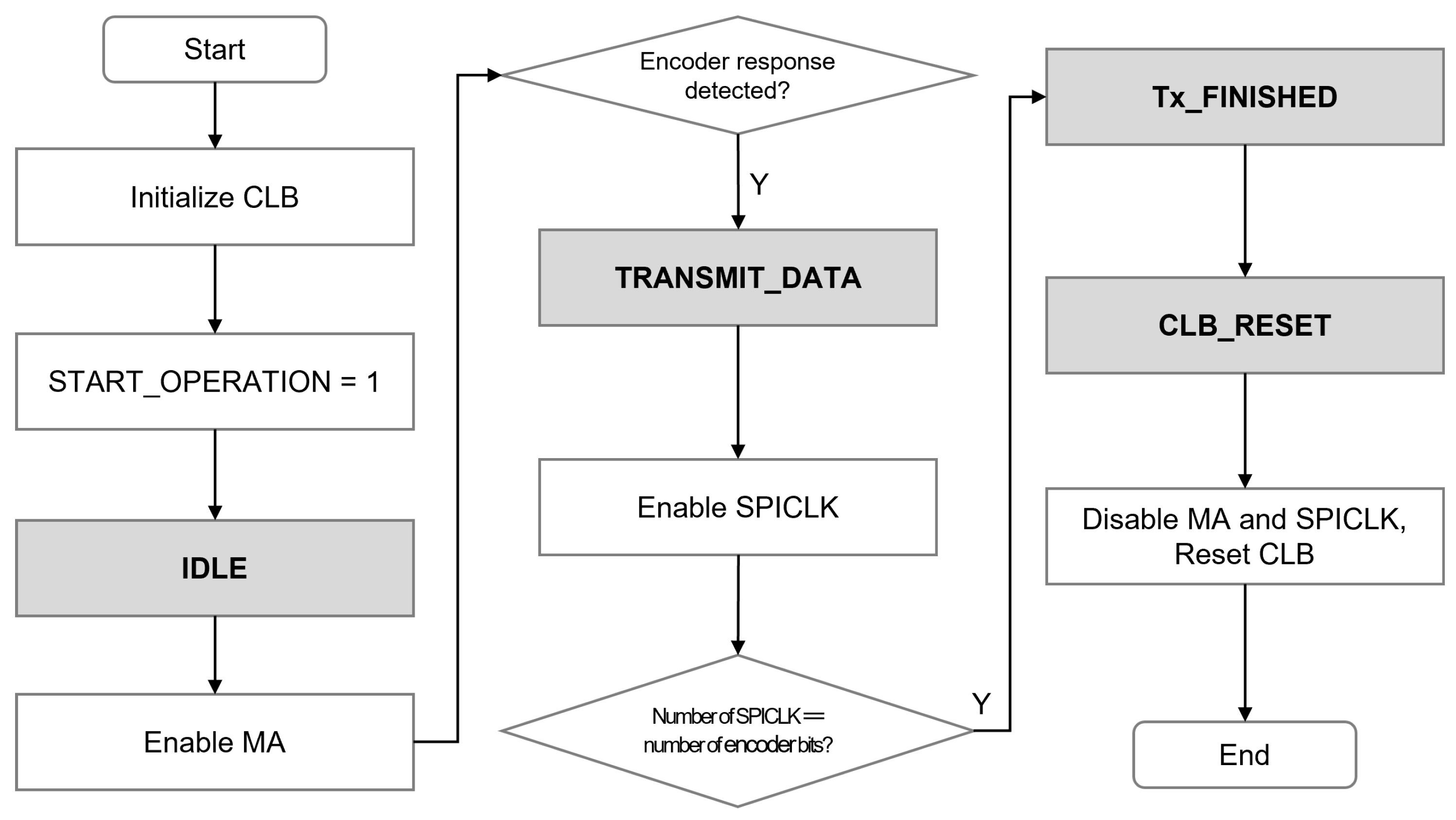
3.3. Main FSM
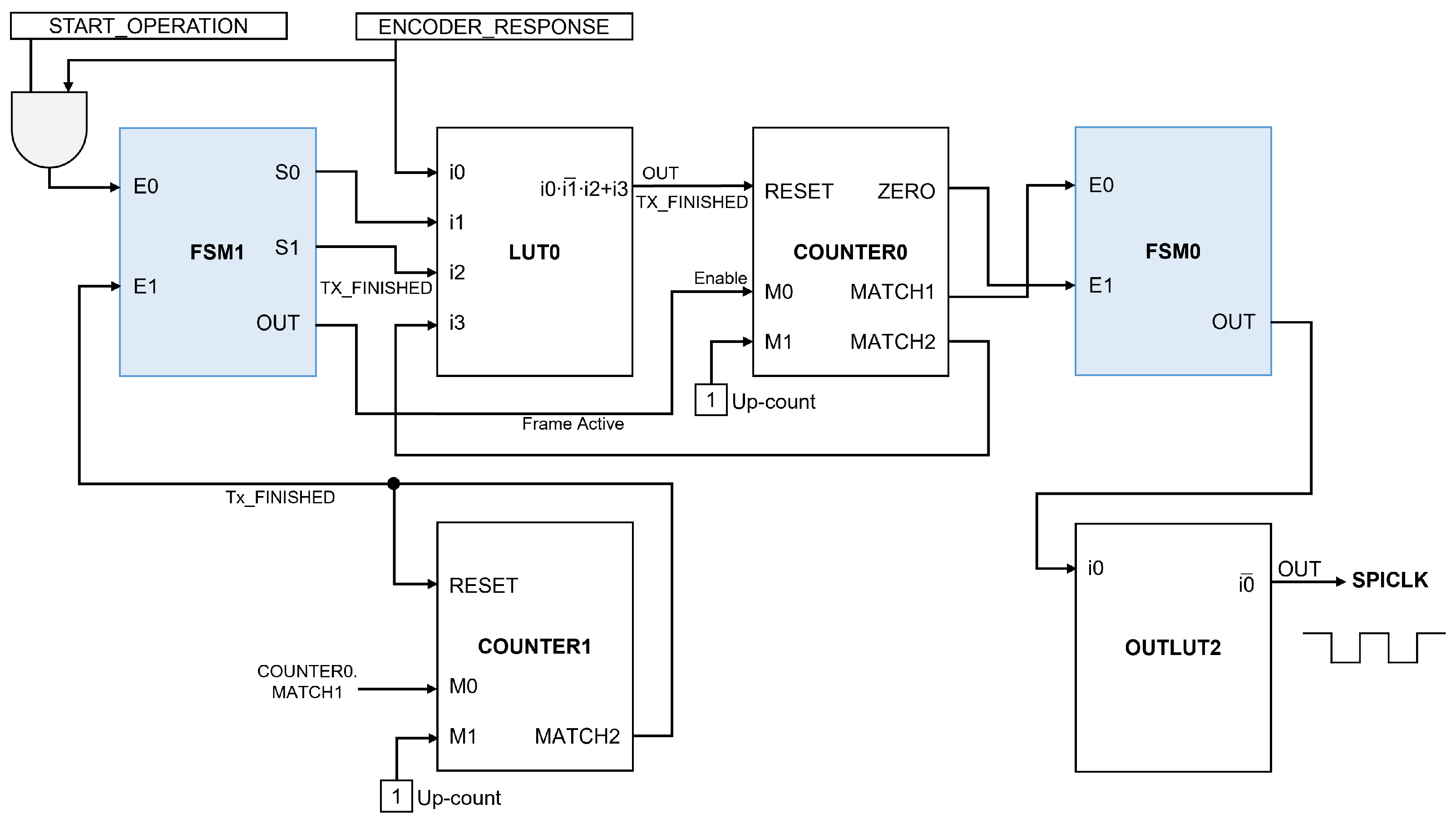
The main FSM denoted by FSM1 is designed to control the entire BiSS-C interface operation. As shown in
Figure 10, the state diagram of FSM1, FSM1 is designed by establishing four states, IDLE, TRANMIT_DATA, TX_FINISHED, and RESET_CLB; two inputs, E0 and E1; and one output, OUT. FSM1 is provided with two binary bits, S0 and S1 for state assignments, and the four FSM1 states are encoded with S0 and S1 as shown in
Figure 10. In the following, the FSM1 design and the operation at each state are described in detail.
3.3.1. IDLE State
The IDLE state is involved with two external events, START_OPERATION and ENCODER_RESPONSE. START_OPERATION is periodically activated by EPWM ISR executed in the motor control program, which implies that START_OPERATION is synchronized with the motor control cycle. ENCODER_RESPONSE is activated when the first rising edge takes place in the SLO signal that indicates the start of the slave frame.
When START_OPERATION is activated in the IDLE state, the MA signal is generated and triggers the slave encoder to start to send the slave frame. Namely, the MA signal should be generated in synchronization with the START_OPERATION event, which is implemented by connecting START_OPERATION to the enable input (M0) of COUNTER2 as shown in
Figure 11. Note that the MA is implemented by COUNTER2 and FSM2 in the design.
The slave encoder receives the MA signal and starts to send the data frame immediately. Then, in the master, the first rising edge of the slave frame is detected, and the ENCODER_RESPONSE event is activated. When START_OPERATION is overlapped with ENCODER_RESPONSE, the IDLE state is changed to the TRANMIT_DATA state, which is implemented by establishing the input equation for the E0 input of FSM1 as follows:
3.3.2. TRANMIT_DATA State
In the TRANMIT_DATA state, the SPICLK signal should be generated to receive the slave data. COUNTER0 and FSM0 are used for SPICLK, and the enable input of COUNTER0 should be connected to the indication of the TRANMIT_DATA state. The TRANMIT_DATA state is indicated by the following output equation of FSM1:
which is connected to the enable input of COUNTER0. After completing to receive the SLO data frame, SPICLK should be stopped, which can be implemented by employing another counter, COUNTER1. Because the SLO frame size of the motor encoder used in this study is 47 bits, the MATCH1_REF and the MATCH2_REF of COUNTER1 are set as zero and 48, and the enable input is connected to the MATCH1 output of the SPICLK COUNTER0. It is noted that the MATCH2_REF of COUNTER1 is set as 48 instead of 47 because the number of SPICLK pulses should be multiples of 8 to match the configured number of SPI data transmission bits. Then, the MATCH2 output of COUNTER1 is activated every 48 bits of a received data, and this MATCH2 output is established as the input, E1, of the FSM1 as follows:
Accordingly, once the E1 input of FSM1 is activated, the TRANMIT_DATA state is changed to the TX_FINISHED state, where COUNTER0 and COUNTER1 should be reset and disabled. Considering this operation process, the structure of the SPICLK generation logic is designed as shown in
Figure 12.
3.3.3. TX_FINISHED and CLB_RESET States
In the TX_FINISHED state, an HLC interrupt is generated by the MATCH2 output of COUNTER1 that is activated at the end of the TRANMIT_DATA State. After the HLC interrupt occurs, the TX_FINISHED state is changed to the CLB_RESET state without any condition. Then, the CLB reset function is executed, and a cycle of receiving the slave encoder data is completed. The structure of COUNTER1 and HLC is shown in
Figure 13, and the timing chart of SPICLK, MATCH1 of COUNTER0, and SLO is shown in
Figure 14, where the instance of the CLB reset is confirmed after completing to receive the 47-bit slave encoder data. In addition, the flowchart of a cycle of receiving the SLO frame is summarized in
Figure 15.
3.3.4. FSM1 Implementation
Reflecting the previous description of the FSM1 operation process, the state table for the FSM1 is shown in
Table 2. Applying the logic reduction technique to the Karnaugh maps, the final logic equations for the next states are derived as follows:
5. Conclusions
We develop a CLB-based BiSS-C interface master for motor control systems that require high-precision and high-speed performance for real-time processing. By analyzing the BiSS-C interface protocol in detail, the truth and state tables are obtained for FSM and logic circuit designs which are required for the master implementation. By programming the CLB sub-modules, the designed FSMs and logic circuits are implemented to generate MA and SPICLK signals and realize the operation process of the BiSS-C master interface.
The developed master turns out to be cost-efficient because an external logic programming device, such as FPGA or CPLD, is not required, which reduces the number of IC parts, PCB size, artwork complexity, and power consumption. It is also beneficial that the developed method can be applied to developing and testing motor drive systems with CLB-integrated MCUs and BiSS-C encoders. Moreover, the developed method can be used to improve the encoder data processing efficiency for the control and diagnostics of various industrial motor systems in automated factories.
The performance and practical usefulness of the developed master are verified by performing various experiments using a built AC motor control system. The maximum master clock frequency without any CRC errors is achieved by 6.25 MHz, which can cope with more than 20 kHz motor control cycle frequency. The usefulness is demonstrated by showing the motor speed and position control performance results that are acceptable in real applications.
As future works, we suggest the following two issues. First, the MA frequency needs to be increased up to 10 MHz by improving the transceiver hardware with a faster speed and finely tuning the SPI interface program. Second, the FPGA- or CPLD-based BiSS-C interface master needs to be built to verify the developed master performance more clearly by comparing the performance results between the developed CLB-based and FPGA- or CPLD-based BiSS-C interface masters.


