Article

LazyRS: Improving the Performance and Reliability of High-Capacity TLC/QLC Flash-Based Storage Systems Using Lazy Reprogramming

School of Computer Science and Engineering, Kyungpook National University, Daegu 37224, Republic of Korea
*
Author to whom correspondence should be addressed.
Electronics 2023, 12(4), 843; https://doi.org/10.3390/electronics12040843
Submission received: 2 January 2023 / Revised: 29 January 2023 / Accepted: 31 January 2023 / Published: 7 February 2023

Abstract

:
We propose a new NAND programming scheme called the lazy reprogramming scheme (LazyRS) which divides a program operation into two stages, where the second stage is delayed until it is needed. LazyRS optimizes the program latency by skipping the second stage if it is not required. An idle interval before the second stage improves the flash reliability as well. To maximize the benefit of LazyRS, a LazyRS-aware FTL adjusts the length of an idle interval dynamically over changing workload characteristics. The experimental results show that the LazyRS-aware FTL can efficiently improve the write throughput and reliability of flash-based storage systems by up to 2.6 times and 31.2%, respectively.

1. Introduction

With rapid growth of the data-driven economy, there are strong needs for high-performance, high-capacity storage systems that can support the core requirements of many emerging data-intensive applications (e.g., business analytics and real-time machine learning). Although there are several examples of memory technology that compete for data-intensive applications, the mainstream storage solutions are all based on high-capacity NAND flash memory. In order to meet the high-capacity requirement for future storage systems, the NAND flash memory has advanced as well. For example, a recent 3D 4 bit quadruple-level cell (QLC) flash device improved the flash capacity by at least 30% over 3D 3 bit TLC flash devices [1,2,3,4,5].
Although m bit multi-leveling techniques have been successful in increasing the flash capacity, they presented a new challenge at the same time. As m is increased, a flash cell has to manage more program states per cell. In order to meet the flash reliability requirements, more careful programming control is needed to distinguish more states from the same cell, which in turn significantly increases the program time. Figure 1a shows how the flash performance has degraded as finer multi-leveling techniques are used. For example, while m was increased from 1 (SLC flash) to 3 (TLC flash), the write throughput degraded to less than half its original value because of an increase in the program latency (tPROG). With the recent QLC flash memory, the slow down in tPROG is further aggravated. For example, the tPROG of QLC flash memory is more than 10 times longer than that of MLC flash memory [2].
The common solution for the poor program performance of high-capacity flash memory is to employ a high-speed internal buffer area, known as hybrid SSD technology (e.g., SLC/MLC hybrid SSD) [6,7,8,9]. This technique uses a small region of the flash memory as an SLC-mode buffer that can operate much faster than MLC operation. When write requests are issued, data are first written to the SLC buffer with a fast write speed, and if the SLC buffer is full, then the data that still remain valid in the SLC buffer (e.g., cold data) are migrated to a high-density MLC region. However, due to the area dedicated to the SLC buffer, the reduction in user capacity cannot be avoided, thus significantly increasing the total cost of the storage system. Furthermore, when the SLC buffer is full, the tPROG of the MLC flash memory will be exposed, which in turn inevitably slows down the write speed. As shown in Figure 1b, our evaluations using a real SLC/QLC NVMe 128 GB SSD [10] show that the write speed quickly dropped when the SLC buffer was full. Since the performance gain achieved by adopting the SLC buffer scheme is limited, hybrid SSD technology loses many opportunities to optimize the flash performance, and therefore it cannot be an efficient solution for high-capacity flash memory.
In this paper, we propose a new system-level optimization technique to enhance the program performance of high-capacity TLC/QLC flash memory without sacrificing the flash capacity and reliability. Our proposed scheme is based on a new NAND programming scheme called the lazy reprogramming scheme ( LazyRS ), which divides the consecutive program process into two separate stages (the turbo stage stage_t and the secure stage stage_s) with an idle interval. In order to improve the tPROG, we exploit a simple observation that not all pages (In NAND flash memory, the page is the unit of read and write operations, and hundreds of pages (e.g., 576 pages [11]) compose a block, the unit of erase operations.) need to be reliably stored to satisfy the worst data retention requirement (e.g., 1 year at 30 ° C in the JEDEC Standard) [12]. By dividing the program operation into two stages, varying data retention requirements can be better matched with different program speeds. When a page is short-lived, stage_t with a fast program speed can be sufficient to meet its retention requirement. Since this page becomes invalidated quickly, it does not need to perform the second stage stage_s. By skipping stage_s, the tPROG can be effectively reduced to the latency of stage_t. However, when a page needs to be long-lived, stage_t alone will not be sufficient to meet the data reliability requirement. For such pages, stage_s is needed to secure the retention requirement. Our proposed LazyRS performs stage_s in an overwrite fashion (i.e., an i n - p l a c e update). This is different from other existing techniques (such as that in [13]) which exploit multiple write modes to enhance the flash performance. Since they perform a reprogramming process in an out-of-place update fashion (i.e., reprogram data into another flash block), many extra writes are triggered, resulting in a significant performance overhead. However, in our LazyRS, no extra writes occur, which effectively eliminates the performance overhead. In a two-stage reprogramming scheme, therefore, the key design consideration is how long two stages should be separated. For example, the shorter an idle interval between two stages, the more stage_s should be applied. A short idle interval between two stages means that the guaranteed retention capability of stage_t is extremely short, such as 1 day. If the data are still valid after 1 day, then all stored data should be rewritten by stage_t to ensure data integrity. As a result, stage_s is more frequently invoked as an idle interval gets shorter. On the other hand, if an idle interval is too long to obtain the proper time for stage_s, then data may be lost before stage_s. In our proposed scheme, the maximum length of an idle interval between two stages is adaptively changed over varying characteristics of data lifetime requirements.
Based on the proposed LazyRS, we have implemented a LazyRS-aware FTL (FTL is an abbreviation for flash transition layer. The FTL is a software layer (a type of firmware) that allows the host’s file system to treat the SSDs as conventional block devices (e.g., HDDs). The FTL performs several key functions to enable SSDs to work in practice, for such as managing logical-to-physical (L2P) mapping information, garbage collection and wear-leveling.) called lazyFTL, which can improve the flash performance without sacrificing data integrity. Our experimental results using various benchmark workloads show that lazyFTL can enhance the overall write throughput by up to 2.6 times over the conventional reprogramming-based FTL. In addition, lazyFTL also improves the flash reliability by up to 31.2% because new reliability concerns in 3D NAND flash memory (e.g., early charge loss) can be efficiently removed due to an idle interval between two stages.
The rest of this paper is organized as follows. In Section 2, we review the relationship between multi-level flash memory and the tPROG. Section 3 describes the proposed LazyRS scheme. In Section 4, we present a design and implementation of lazyFTL. The experimental results follow in Section 5, and the related work is summarized in Section 6. Section 7 concludes with a summary and future work.

2. Background

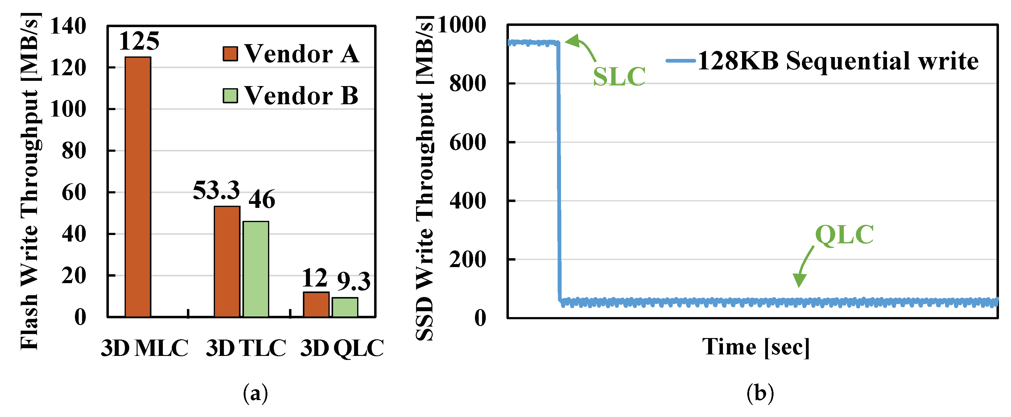
2.1. Multi-Level Flash Memory vs. Program Latency

Figure 2 illustrates the V t h distributions for 2 m -state NAND flash memory, which stores m bits within a single flash cell by using 2 m distinct V t h states (i.e., m is two and four for MLC and QLC, respectively) (The threshold voltage, commonly abbreviated as V t h , of a normal MOS transistor is the minimum gate-to-source voltage ( V G S ) that is needed to create a conducting path between the source and drain terminals. When V G S is larger than V t h , a transistor can flow the electrical current (i.e., turn-on state) and vice-versa. As a result, a transistor can work like a switch. Although the NAND cell is structurally similar to a normal MOS transistor, it is unique in that it can change its threshold voltage ( V t h ) by injecting or ejecting electrons). For writes, flash memory changes the target cell’s V t h state based on the content information (per bit). For example, MLC flash can store ‘01’ data (MSB page = ‘0’, and LSB page = ‘1’) by raising the flash cell’s V t h level to 3V (i.e., P3 state). In order to read the stored data from flash cells, the V t h level of the flash cells is probed by using a read reference voltage V r e f . The ‘01’ data can be successfully reconstructed by sensing the V t h level of the flash cell with V r e f R 3 .
As m is increased, more V t h states should be put into the limited V t h window ( W t o t ), which is fixed at the flash design time. Therefore, the V t h margin (The amount of the V t h margin is calculated as W t o t i = 0 k W P i .) (i.e., a gap between two neighboring V t h states) inevitably becomes narrower, as shown in Figure 2a,b. When the V t h margin gets smaller, the flash memory becomes more vulnerable to various noise effects (e.g., P/E cycle (Repetitive program and erase operations, denoted as P/E cycles, cause wear of flash cells due to high-voltage stress during operations.) or retention time), resulting in reliability degradation. As shown in Figure 2, the amount of the V t h margin is determined by the width of the program states ( W P i ). Hence, to guarantee the reliability requirements of multi-level cell flash memory, W P i should be kept as narrow as possible to ensure the sufficient V t h margin [14].
NAND flash memory generally employs the i n c r e m e n t a l s t e p p u l s e p r o g r a m m i n g (ISPP) scheme [15] to control the W P i of program states. The ISPP scheme gradually increases the program step voltage by Δ V i s p p at a time until all flash cells are completely programmed. As a result, the tPROG can be defined as follows:
t P R O G ( V e n d V s t a r t ) Δ V i s p p
where V e n d and V s t a r t are the final program step voltage and the start program step voltage, respectively.
Since W P i is proportional to Δ V i s p p , a straightforward solution to ensure a sufficient V t h margin is to narrow the W P i by reducing the Δ V i s p p during a program’s operation [16]. Unfortunately, although the Δ V i s p p reduction can improve the flash reliability, it can also directly increase the tPROG, as shown in Equation (1). Therefore, for high-capacity multi-level flash memory, performance degradation cannot be avoided to secure the flash reliability requirements.

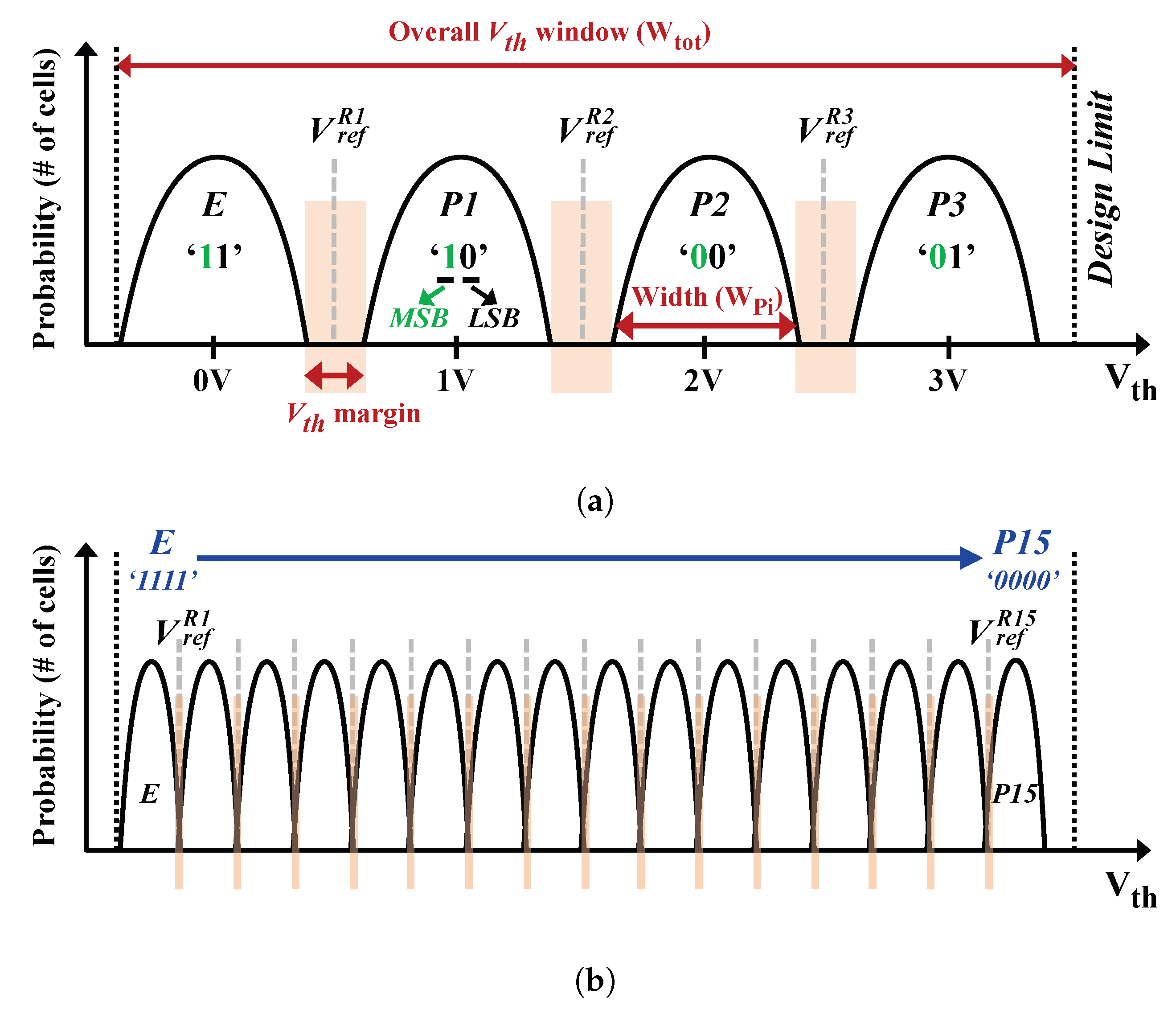
2.2. Conventional Reprogramming Scheme

Reprogramming is a popular NAND programming scheme which has been widely employed in recent flash devices [1,17,18]. The main goal of the reprogramming scheme is to minimize the negative effect of various noises, such as program disturbance, early charge loss and wordline ( W L ) interference, thus preventing the reliability degradation of high-capacity multi-level flash memory (e.g., TLC or QLC flash memory) [2]. To suppress these noise effects, the reprogramming scheme performs a program operation with two successive internal steps ( c o a r s e program and f i n e program) and interleaves each step into multiple WLs. (The NAND flash memory has a matrix organization which consists of row-directional wordlines (WLs) and column-directional bitlines (BLs).)
Figure 3a illustrates the program sequence used in the representative 2 step 16-16 QLC reprogramming scheme, where 16 V t h states are programmed in both coarse and fine programs. We denote the nth wordline in a flash block as W L ( n ) . Initially, W L ( n ) is coarsely programmed to a lower V t h level than the final target level using a large Δ V i s p p (➊). Next, the neighboring W L ( n + 1 ) is programmed in the same way (➋). As shown at the top of Figure 3b, during the coarse program of neighboring W L ( n + 1 ) , the V t h distribution of W L ( n ) is widened and shifted due to the noise effects. To eliminate these effects, the W L ( n ) is finely programmed with a small Δ V i s p p (➌). The bottom of Figure 3b illustrates the final V t h distribution after completing the fine program. Since the fine program enables a narrow V t h state in a noise-free way, NAND flash memory can ensure flash reliability even in high-capacity multi-level flash memory.

3. LazyRS: Lazy Reprogramming Scheme

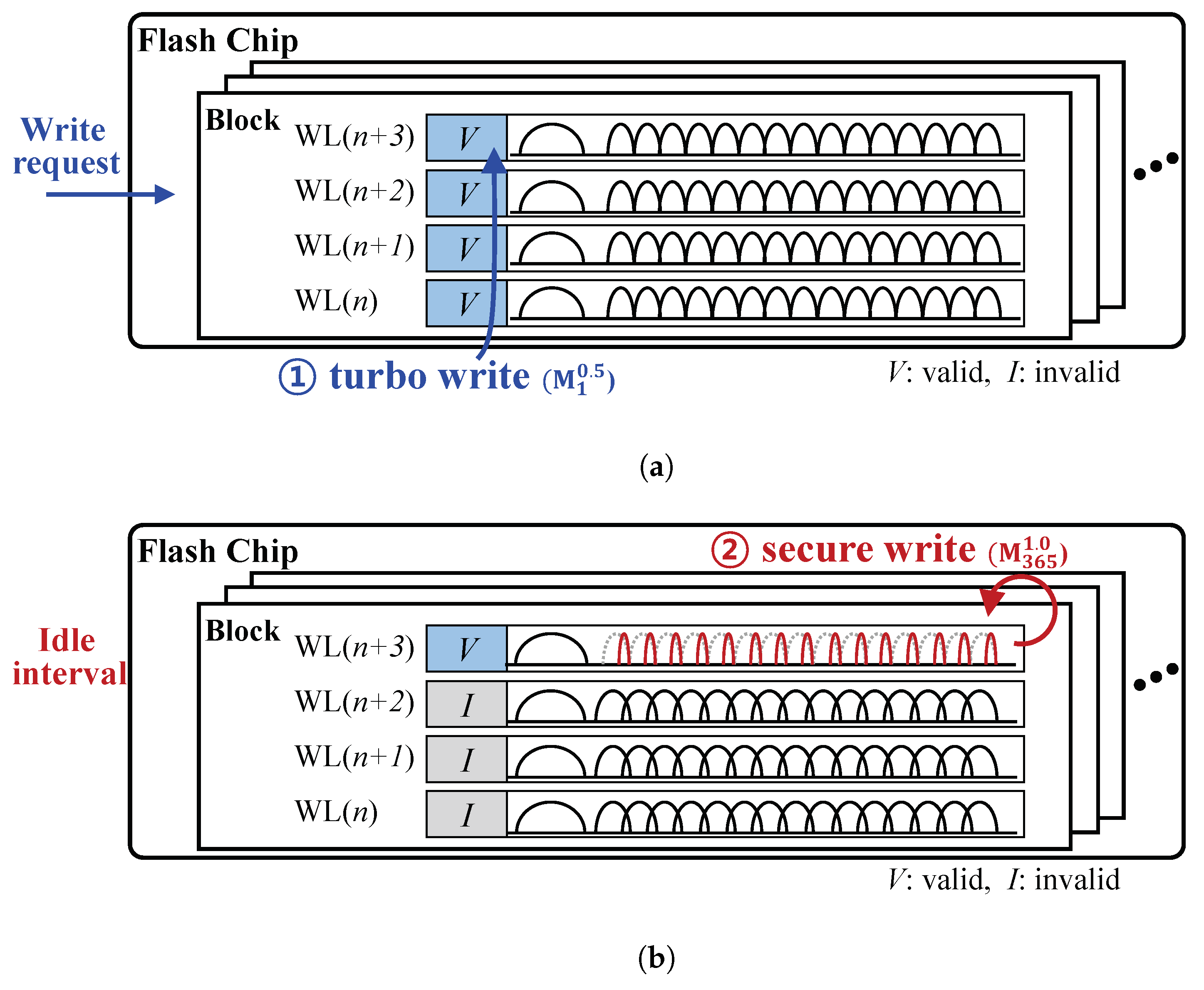
3.1. Basic Idea of the LazyRS

Typically, NAND flash memory is designed to secure perfect data integrity 100% of the time. For all data, NAND flash memory performs the program operation in an error-resistant way (i.e., keeping the program states narrow as much as possible using a small Δ V i s p p ) to ensure flash reliability even in the worst-case conditions (e.g., 1 year retention after maximum P/E cycles). However, since most data used in modern computing systems (e.g., deep learning or key value DB) have a short lifespans of less than 1 day or 1 week, this conservative approach causes a significant cost in terms of performance and loses many opportunities to further optimize the performance of flash-based storage systems.
Our LazyRS is motivated by the observation that the internal consecutive program process of the conventional reprogramming scheme can be divided into two independent program stages (the turbo stage stage_t and the secure stage stage_s) with asymmetry in program latency and retention capability. Stage_t enables fast program operation but is less reliable. On the other hand, stage_s ensures perfect data integrity with a relatively slow write speed. By leveraging two program stages and an idle interval, our LazyRS can efficiently optimize the overall performance of flash-based storage systems without any hardware modification. (LazyRS can be implemented by exploiting the conventional reprogramming scheme.)
Figure 4 illustrates the key idea of the LazyRS scheme, assuming that two turbo stages (M 1 0.5 and M 30 0.7 ) and one secure stage (M 365 1.0 ) can be used. M t s indicates that data are programmed with (1 − s) × 100% faster latency and a t day retention capability. For example, M 30 0.7 can write data 30% faster while guaranteeing a 30 day retention capability, which means these data cannot be read correctly after 30 days. As shown in Figure 4, when write requests are issued from the host system, all data are written first in stage_t using M 1 0.5 (➀). By forming wide program states, M 1 0.5 can achieve 50% faster program latency. Since stage_t of M 1 0.5 can guarantee only 1 day of retention, the data which remain valid after one day should be reprogrammed in stage_s to ensure the data’s integrity (➁). However, if the data are invalidated within one day, then the program performance can be doubled because there is no need to run stage_s. Even if stage_s cannot be skipped due to the remaining long-lived data, they can be effectively hidden during an idle interval between two stages. Therefore, the effectiveness of the LazyRS can be retained. In our LazyRS, an idle interval is decided by the retention capability of stage_t.
When large amounts of data remain alive for a long time (e.g., read-intensive workload) or an idle interval is not sufficient to hide stage_s, the effectiveness of our scheme is restricted because the program latency of the slow stage_s is revealed. (Even if stage_s is exposed, the overall performance of our LazyRS is not worse than conventional reprogramming.) Therefore, in order to ensure the effectiveness of the LazyRS, it is essential to suppress the occurrence of stage_s. Our LazyRS manages how much data should be reprogrammed in stage_s using a data structure called the difference list (detailed in Section 4). If the amount of data to be reprogrammed exceeds a certain level, then the condition of stage_t can be switched from M 1 0.5 to M 30 0.7 , which can guarantee a longer retention capability (1 week), thus efficiently reducing the long-lived data that require stage_s. By dynamically selecting the stage_t conditions over changing workload characteristics, the LazyRS can further optimize the flash performance.

3.2. LazyRS-Aware NAND Retention Model

In order to take advantage of the LazyRS scheme at the FTL level, it is crucial for an FTL to understand the reduced retention capability of stage_t. To construct the NAND retention model, we conducted comprehensive evaluations using 160 state-of-the-art 3D flash chips which were fabricated by 3D VNAND CT (charge trap) technology, known as SMArT [19] or TCAT [20]. In our characterization study, we used 48 layer 3D TLC flash chips from the same NAND flash manufacturer. Although there are multiple 3D TLC flash manufacturers in the market, all the commercial 3D NAND flash memories from these manufacturers have similar structures and cell types (e.g., vertical channel structures, gate-all-around transistors and charge trap cell types) [19,20]. It is commonly believed that different 3D TLC flash chips share key device-level characteristics. Therefore, our characterization results would be highly relevant and applicable to most commercial 3D TLC flash chips in the market.
To minimize the potential distortions in the evaluation results, we evenly selected 128 test blocks from each chip at different physical block locations and tested all the WLs in each selected block. As a result, a total of 20,480 blocks and 11,059,200 pages were tested to obtain statistically significant experimental results. By using an in-house custom test board (equipped with a flash controller and a thermal controller), we evaluated the retention errors N r e t ( t ) under various operating conditions. To ensure the confidence of reliability tests, we followed the JEDEC standard [21] recommended for commercial-grade flash products. The retention errors especially were measured by using an accelerated lifetime test based on the Arrhenius relationship [22]. For example, the effect of the 12 month retention time at 30 ° C could be converted to the 13 h retention time at 85 ° C. In addition, to avoid data pattern dependency, we used a pseudo-random pattern in writing the data to NAND flash memory [23]. Although our evaluations were based on TLC flash chips, their validity can be also applied to QLC flash memory.
Figure 5a shows how the program latency of stage_t can be improved when the retention capability is relieved. As a measurement metric of the retention capability, we used the NAND retention bit error rate (BER), which is based on the number N r e t ( t ) of retention errors after a t day retention time for 1000 P/E cycles. (Typically, it is known that TLC flash can tolerate 1000 P/E cycles.) We examined N r e t ( t ) values with increasing Δ V i s p p . The program latency of each condition was determined when N r e t ( t ) reached 90% error correction code (ECC) capability. (When a flash page is read, a flash controller can correct a certain number of bit errors (e.g., up to 60 bit errors per 1 KB of data) by using an error correction code (ECC) engine [24].) The baseline was the program latency of the conventional reprogramming scheme which ensures the 1 year retention capability. Our evaluation results show that the more the retention requirement was relieved, the faster the program latency became possible. If we designed stage_t with the 1 week retention capability, the program latency could be significantly enhanced by more than 60% compared with that of the conventional reprogramming scheme.
Figure 5b shows that LazyRS can improve flash reliability as well as flash performance. In LazyRS, the data written in stage_t experience a certain amount of an idle interval before entering stage_s. This idle interval enables LazyRS to mitigate the impact of early charge loss on flash reliability. The phenomenon of early charge loss, which is not shown in 2D flash memory, unexpectedly changes V t h states of flash cells just after a program operation completes, thus significantly increasing the bit errors in 3D flash memory [25]. Our evaluation results show that as an idle interval increased, the effect of early charge loss was suppressed, so the data written in stage_s became more reliable. For example, if the 1 month idle interval were applied, the flash reliability could be improved by up to 31.2% compared with that of the conventional reprogramming scheme.

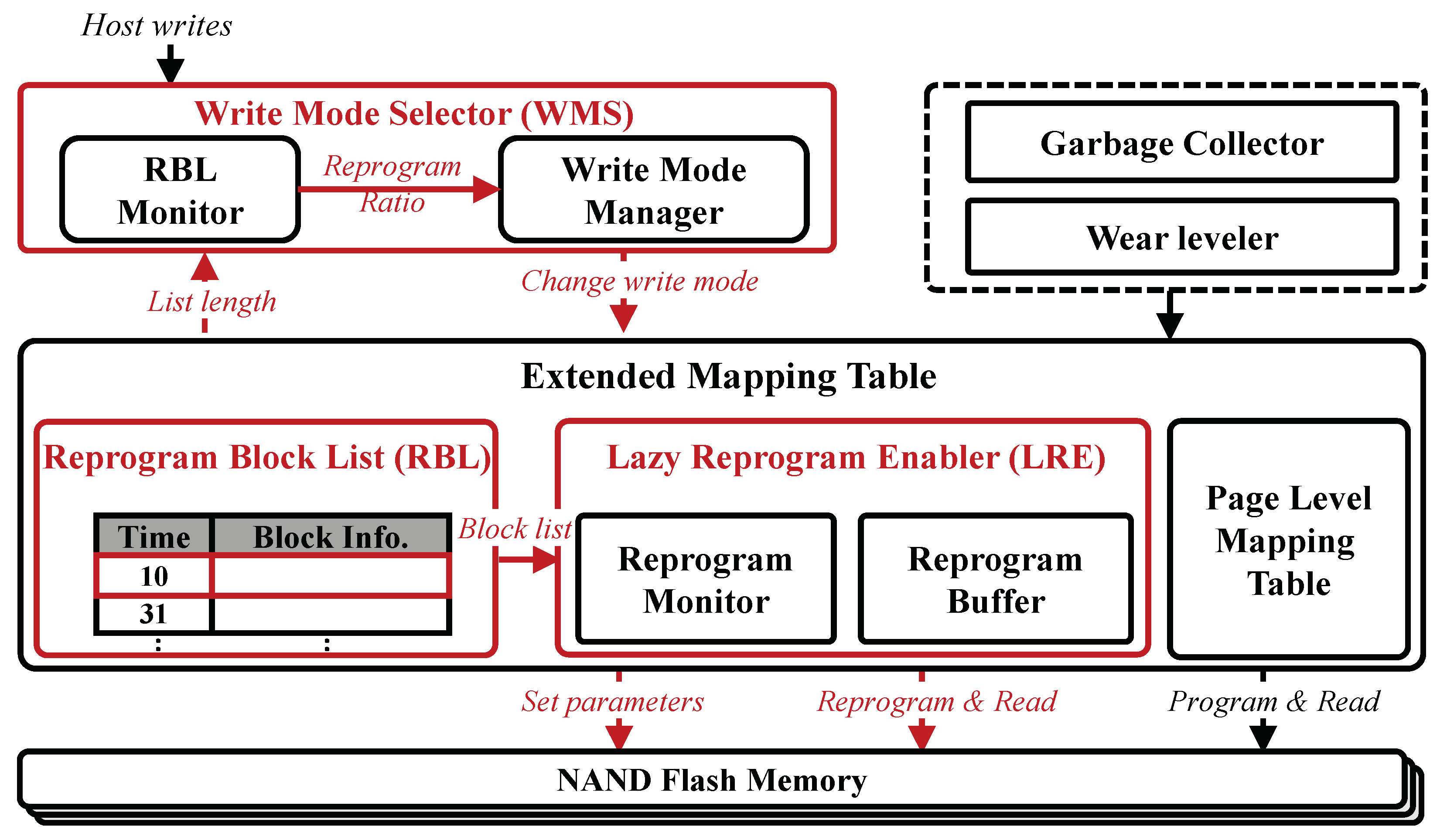
4. LAZYFTL: LazyRS-Aware FTL

Based on our LazyRS-aware NAND retention model described in Section 3, we implemented lazyFTL, a new LazyRS-aware FTL, where lazyFTL is based on an existing page-level mapping FTL with additional modules for efficiently managing our LazyRS features. In this section, we first explain the overall architecture of lazyFTL and then give detailed explanations for each module.
Figure 6 illustrates an organizational overview of lazyFTL. When a host write arrives, a write mode selector (WMS) chooses a proper write mode to execute stage_t. This write mode selection is made by referring to the status of a reprogram block list (RBL), which reflects the workload characteristics. The RBL also keeps track of data that were programmed in stage_t and then decides when to trigger the reprogramming. If the data that should be reprogrammed in stage_s are found, then their physical addresses are transferred to a lazy reprogram enabler (LRE) which performs the secure stage_s.

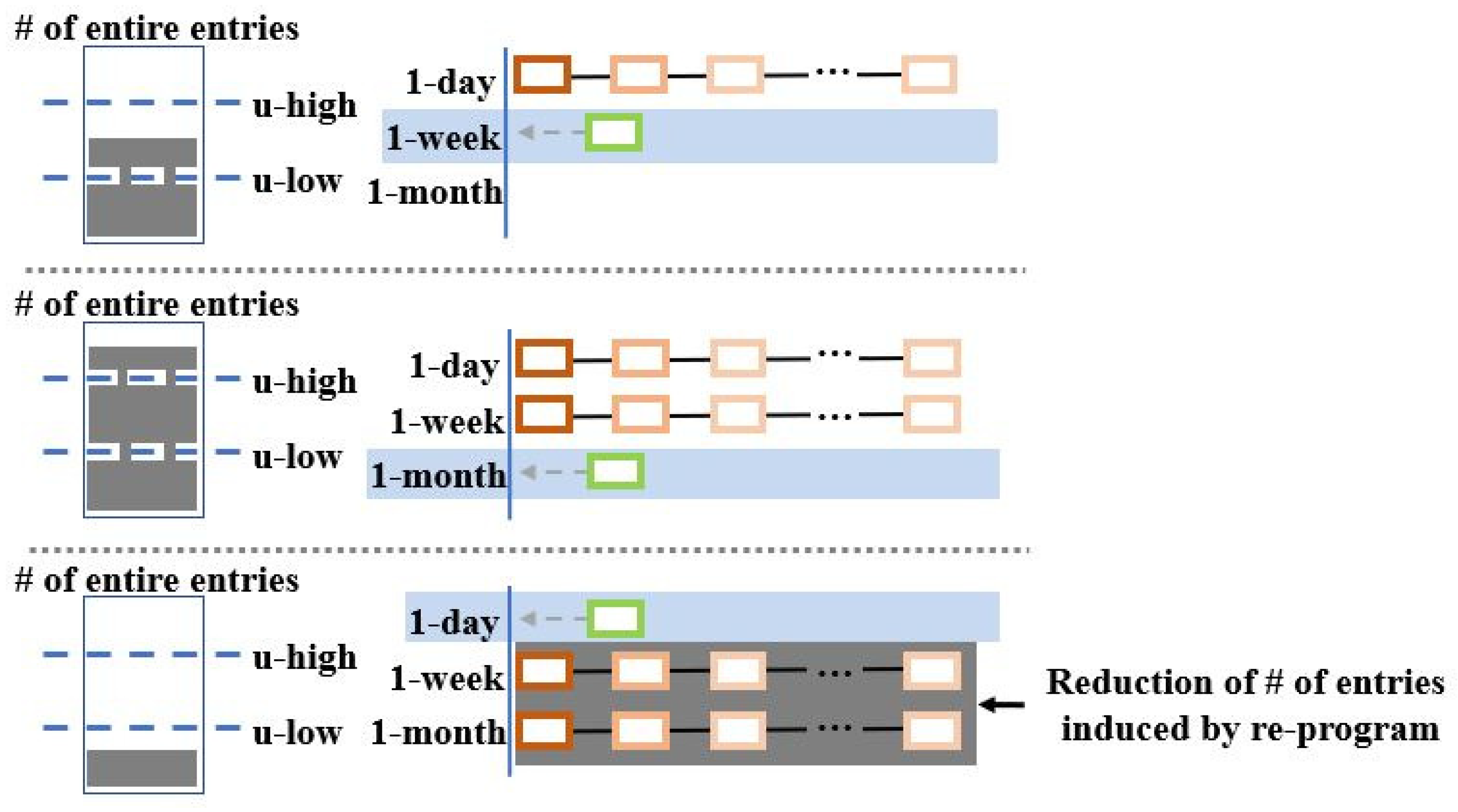
4.1. Reprogram Block List (RBL)

In order to take full advantage of the proposed techniques, the RBL manages the data to be reprogrammed in stage_s on a per-block basis. (We expect that all the pages in the same flash block are programmed at a similar time.) It is not efficient to monitor all the flash blocks regularly. Instead, the RBL maintains a tiny list of blocks that hold data which should be reprogrammed in the future. In this way, it minimizes block monitoring overheads.
Figure 7a,b describes an operational overview of how the RBL manages a list. When a new flash block becomes active (i.e., when data are first written to it in stage_t), the RBL adds a write time and the block’s information to the tail of the list. After all of the free pages in the current active block are used up, another free block becomes active and is pushed to the tail of the list. Then, new data are written to the new active block. As a result, the head entry in the list points to the oldest block holding data that should be reprogrammed at the earliest time.
If the head entry needs to enter stage_s, and the flash block has valid data, then the entry information is passed to the LRE, which actually performs stage_s reprogramming (see Section 4). The entry is then deleted from the RBL. If the flash block has no valid data, then the RBL does not trigger stage_s and only deletes the head entry. There is a possibility that some flash blocks may be garbage-collected and erased. In that case, it is unnecessary to maintain entries for erased blocks in the list, and the RBL should remove them from the list. The block list in the RBL is combined with a hash data structure, so the RBL can quickly find an erased block entry in the list by using its block number as a hash key.
As explained in Section 3, an idle interval is determined by the retention capability of stage_t’s write mode. Since there are three modes in our lazyFTL, the RBL should manage three lists for different write modes. Even in the worst case, the total number of the RBL entries does not exceed the number of flash blocks in an SSD. When an SSD’s capacity is 128 GB, the amount of DRAM for the lists does not exceed 192 KB at most.

4.2. Write Mode Selector (WMS)

The main role of the WMS is to set an optimal write mode for the stage_t program. In our study, three write modes (M 1 0.3 , M 7 0.4 and M 30 0.5 ), which were derived from the NAND retention model, were used for stage_t (As mentioned in Section 4, there is a strong inverse relationship between tPROG and flash reliability. Based on these well-known flash characteristics, we can design a vast number of write modes depending on how much retention capability is restricted. For example, we can make different write modes that secure x days of retention time by varying the value x. In our paper, we selected three write modes based on the workload characteristics used in the experiments. The workload characteristics are analyzed in Section 5). When the write mode is selected, the WMS transfers the corresponding operation parameters { V i s p p 1 s t , V r e f 1 s t } to the NAND flash memory to perform stage_t. Our lazyFTL uses M 1 0.3 by default, which has 70% faster program latency with the data retention capability of only a single day.
The write mode should be carefully decided, depending on the characteristics of and changes in a given workload. If the data written with M 1 0.3 survive longer than one day (i.e., they have not been overwritten or invalided in one day), then they are forced to be reprogrammed with stage_s. This inevitably causes extra I/O traffic, which in turn degrades the overall I/O performance. To regulate such extra I/Os, the WMS changes the write mode to M 7 0.4 (or M 30 0.5 ), which has a longer retention capability.
The write mode is determined by the length of the RBL u. The WMS maintains two threshold values: u h i g h and u l o w . If u > u h i g h , then this means that many blocks requiring the stage_s program stay in the list, which significantly slows down the performance of the storage system. The more the flash blocks are reprogrammed, the lower the flash performance is. If the length of the RBL exceeds a specific threshold (i.e., u > u h i g h ), then the WMS changes the current write mode to the slower one, which allows a longer retention time to restrict the length of the RBL. (In our experiment, u h i g h and u l o w were 60% and 30% of the entire block entry list length, respectively. In this paper, we fixed the values of u h i g h and u l o w . However, to maximize the performance of storage systems, it is necessary that u h i g h and u l o w be dynamically adjusted depending on the workload characteristics. We plan to study how to decide the optimal RBL parameters in future work.) On the other hand, if u < u l o w , then almost all of the blocks are invalidated before the stage_s program. Thus, the current write mode is promoted to the faster one. Otherwise, the WMS maintains the current write mode (i.e., u l o w < u < u h i g h ). In this manner, the WMS can adapt to changing workloads. Figure 8 demonstrates how the WMS selects the current write mode using two threshold values: u h i g h and u l o w .

4.3. Lazy Reprogram Enabler (LRE)

The LRE module safely performs the secure stage_s program. As explained earlier, the information of a block whose data should be reprogrammed soon is delivered to the LRE. Before executing stage_s, the LRE reads the valid data of the target block which was written with the stage_t program. The read data are temporally stored in the internal buffer, called a reprogram buffer, and then overwritten to the same block at once using stage_s. The operating parameters for the stage_s program are set to { V i s p p 2 n d , V r e f 2 n d } so it can guarantee the same level of the retention capability as the normal NAND program.

5. Experimental Results

5.1. Experimental Settings

In order to evaluate the effectiveness of the proposed technique, we implemented lazyFTL as a host-level FTL using the open flash development platform [26]. This can support a 512 GB flash capacity at maximum, but we limited its capacity to 16 GB for fast evaluations. Our platform consists of two buses, each of which has four TLC NAND chips. Each flash chip has 512 blocks, and each block is composed of 576 pages (16 KB per page).
Three distinct I/O workloads, which were generated by Filebench [27], were used for our evaluations. As summarized in Table 1, the three benchmarks represented different I/O characteristics of various applications with different I/O intensities and read/write combinations. Webproxy is a read-dominant workload representing the I/O activities of a simple web proxy server’s disk I/O. Varmail emulates a mail server, and OLTP is a write-dominant workload which has a small idle interval. To evaluate the impact of lazyFTL on the flash performance, we obtained the trace of each workload and created time intervals.
In our experiments, as mentioned in Section 4.2, we selected three write modes for lazyFTL, M 1 0.3 and M 7 0.4 based on the workload characteristics. Figure 9 shows how much retention time was needed in different workloads. In Varmail, 46% of the total data needed a relatively long retention time of more than 1 month, while we could guarantee the data integrity of about 50% of the data in OLTP with only 1 day for the retention time. The details of the program latency for each write mode and conventional reprogramming scheme are summarized in Figure 9b.

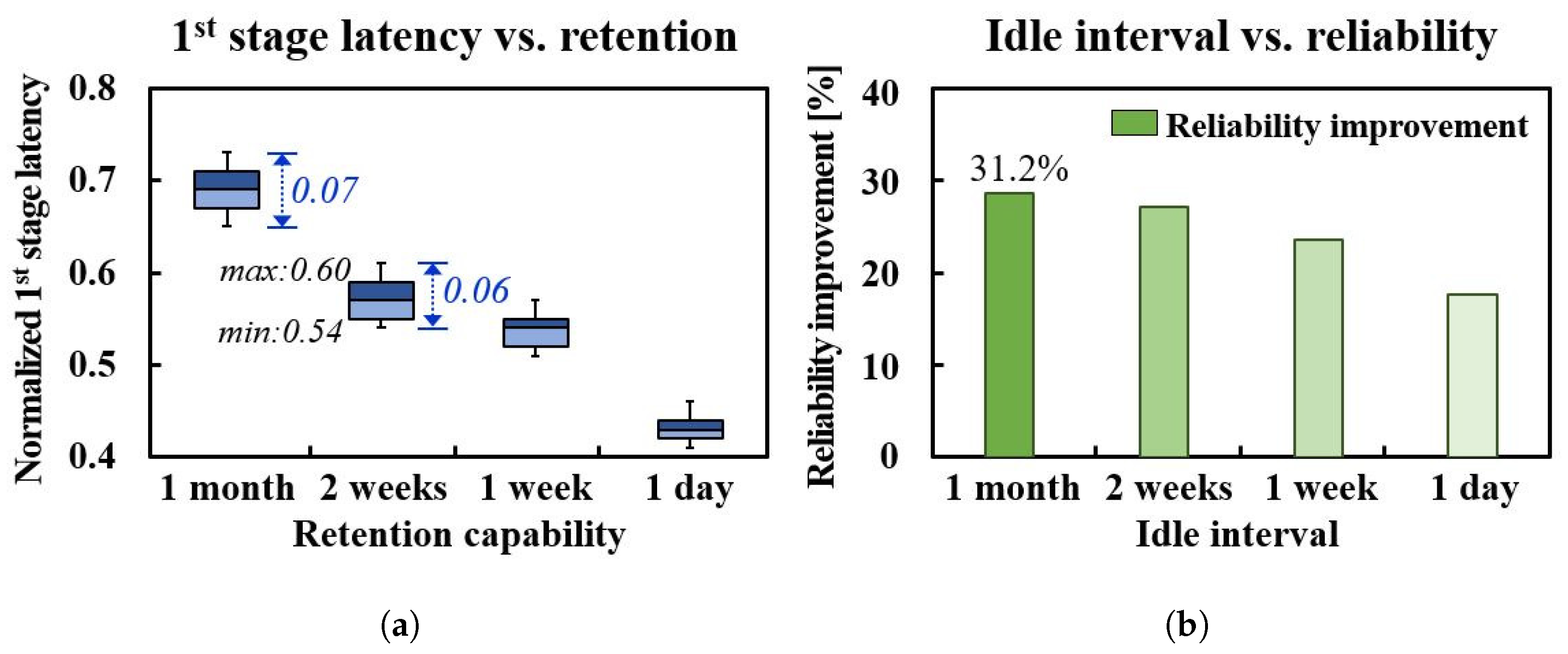
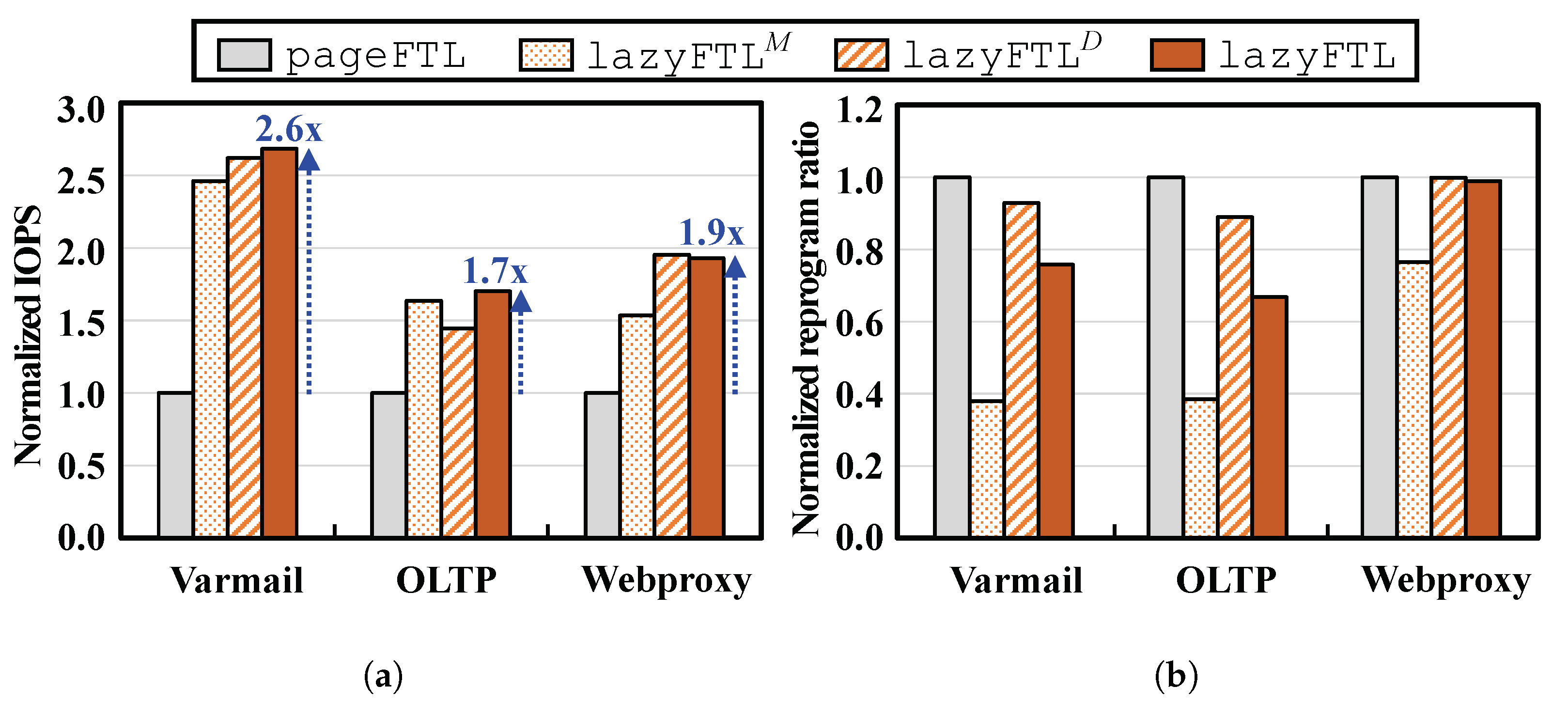
5.2. Experimental Results

To identify the effectiveness of our proposed technique, we compared lazyFTL with the conventional page-level FTL (pageFTL), lazyFTL D and lazyFTL M . lazyFTL D and lazyFTL M are a static type of lazyFTL that exploit only one write mode for stage_t (M 1 0.3 and M 30 0.5 , respectively). We measured the IOPS of the four FTLs under three workloads. As shown in Figure 10a, lazyFTL outperformed pageFTL, lazyFTL M and lazyFTL D by up to 2.6 times, 1.25 times and 1.17 times, respectively. In comparison with pageFTL, lazyFTL improved the IOPS by 2.6 times, 1.9 times and 1.65 times, respectively. In the Varmail and Webproxy workloads, the workload intensity was not much higher, so lazyFTL could utilize a sufficient idle interval to execute stage_s. On the contrary, since OLTP had a high write-intensive workload, it was less efficient for lazyFTL to execute stage_s during the idle interval.
To better understand the different improvements between workloads, we also measured how many runs of stage_s should be performed (i.e., the reprogramming ratio) on each FTL, as shown in Figure 10b. As expected, the reprogramming ratio was the lowest in lazyFTL M because it had the longest idle interval. Among the workloads, since Webproxy is a read-dominant workload, many data remained alive for a long time, making the reprogramming ratio high. This explains why Webproxy exhibited lower performance improvement than Varmail in lazyFTL. On the other hand, since OLTP is a write-dominant workload, its reprogramming ratio was relatively lower compared with the other workloads. Due to the lower reprogramming ratio of lazyFTL compared with lazyFTL D in OLTP, lazyFTL showed better performance than lazyFTL D .

6. Related Works

There have been many studies that attempted to improve the performance of NAND flash memory [13,28]. However, due to various side effects, most existing technologies are limited in their application to modern high-capacity multi-level flash memory. Liu et al. proposed a technique which optimized the performance and ECC cost using the workload characteristics [13]. This technique is similar to lazyFTL in that it exploits multiple write speeds based on the retention capabilities of the workloads. It boosts the host write speed using the retention-relaxed mode with the assumption that most data have short retention requirements. For long-lived data, it is reprogrammed to another flash block with a normal speed. Since this technique should trigger extra writes to ensure no data loss, it will suffer from significant performance overhead and additional wear of the flash devices. In addition, this technique cannot improve new noise effects in 3D flash memory, such as early charge loss. Lee et al. also proposed a technique called correction before coupling (CBC) to enhance the performance of MLC flash memory [28]. By reading the data in the lower WL and correcting its errors by ECC before programming the upper WL, it can improve the performance of the coarse program step. Since each program operation requires additional read and error correction, its applicability is limited in TLC or QLC flash, which has more pages per WL compared with MLC flash.

7. Conclusions

We presented a new system-level technique that tackles the performance problem of high-capacity multi-level flash memory. Our proposed technique is based on the lazy reprogramming scheme, which divides a program operation into two stages with different program latencies and retention capabilities. Since stage_s can be skipped or hidden by exploiting an idle interval, LazyRS can significantly improve the write performance of flash storage systems. Furthermore, the idle interval enables LazyRS to mitigate the impact of the early charge loss on flash reliability. Based on our NAND retention model, we implemented a LazyRS-aware FTL called lazyFTL, which takes full advantage of the LazyRS-enabled flash device. By dynamically adjusting the length of an idle interval over changing workload characteristics, the effectiveness of lazyFTL can be maximized without additional overhead. Our experimental results show that the LazyRS-aware FTL can improve the write throughput and flash reliability by up to 2.6 times and 31.2%, respectively.
The current version of lazyFTL can be extended in several directions for QLC flash memory. For example, we plan to examine a multi-step reprogramming scheme which can support more than two stages. By exploiting the extended version, we believe that it can better optimize high-capacity flash-based storage systems under various user environments.

Author Contributions

Conceptualization, B.K. and M.K.; methodology, B.K. and M.K.; investigation, B.K. and M.K.; resources, M.K.; data curation, B.K. and M.K.; writing—original draft preparation, B.K. and M.K.; writing—review and editing, M.K.; visualization, B.K. and M.K.; supervision, M.K.; project administration, M.K.; All authors have read and agreed to the published version of the manuscript.

Funding

This work was supported by the National Research Foundation of Korea(NRF) grant funded by the Korea government(MSIT) (NRF-2022R1I1A3073170).

Data Availability Statement

Most data in this paper is protected by NDA with NAND manufacturer.

Conflicts of Interest

The authors declare no conflict of interest.

References

  1. Shibata, N.; Kanda, K.; Shimizu, T.; Nakai, J.; Nagao, O.; Kobayashi, N.; Miakashi, M.; Nagadomi, Y.; Nakano, T.; Kawabe, T.; et al. 13.1 A 1.33Tb 4-bit/Cell 3D-Flash Memory on a 96-Word-Line-Layer Technology. In Proceedings of the 2019 IEEE International Solid- State Circuits Conference—(ISSCC), San Francisco, CA, USA, 17–21 February 2019; pp. 210–212. [Google Scholar] [CrossRef]
  2. Lee, S.; Kim, C.; Kim, M.; Joe, S.-M.; Jang, J.; Kim, S.; Lee, K.; Kim, J.; Park, J.; Lee, H.-J.; et al. A 1Tb 4b/cell 64-stacked-WL 3D NAND flash memory with 12MB/s program throughput. In Proceedings of the 2018 IEEE International Solid- State Circuits Conference—(ISSCC), San Francisco, CA, USA, 11–15 February 2018; pp. 340–342. [Google Scholar] [CrossRef]
  3. Takai, Y.; Fukuchi, M.; Kinoshita, R.; Matsui, C.; Takeuchi, K. Analysis on Heterogeneous SSD Configuration with Quadruple-Level Cell (QLC) NAND Flash Memory. In Proceedings of the 2019 IEEE 11th International Memory Workshop (IMW), Monterey, CA, USA, 12–15 May 2019; pp. 1–4. [Google Scholar] [CrossRef]
  4. Goda, A. Recent progress on 3D NAND flash technologies. Electronics 2021, 10, 3156. [Google Scholar] [CrossRef]
  5. Cho, W.; Jung, J.; Kim, J.; Ham, J.; Lee, S.; Noh, Y.; Kim, D.; Lee, W.; Cho, K.; Kim, K.; et al. A 1-Tb, 4b/Cell, 176-Stacked-WL 3D-NAND Flash Memory with Improved Read Latency and a 14.8 Gb/mm2 Density. In Proceedings of the 2022 IEEE International Solid-State Circuits Conference (ISSCC), San Francisco, CA, USA, 20–26 February 2022; Volume 65, pp. 134–135. [Google Scholar]
  6. Im, S.; Shin, D. ComboFTL: Improving performance and lifespan of MLC flash memory using SLC flash buffer. J. Syst. Archit. 2010, 56, 641–653. [Google Scholar] [CrossRef]
  7. Chang, L.P. A Hybrid Approach to NAND-Flash-Based Solid-State Disks. IEEE Trans. Comput. 2010, 59, 1337–1349. [Google Scholar] [CrossRef]
  8. Kwon, K.; Kang, D.H.; Eom, Y.I. An advanced SLC-buffering for TLC NAND flash-based storage. IEEE Trans. Consum. Electron. 2017, 63, 459–466. [Google Scholar] [CrossRef]
  9. Shin, S.-H.; Shim, D.-K.; Jeong, J.-Y.; Kwon, O.-S.; Yoon, S.-Y.; Choi, M.-H.; Kim, T.-Y.; Park, H.-W.; Yoon, H.-J.; Song, Y.-S.; et al. A new 3-bit programming algorithm using SLC-to-TLC migration for 8MB/s high performance TLC NAND flash memory. In Proceedings of the 2012 Symposium on VLSI Circuits (VLSIC), Honolulu, HI, USA, 13–15 June 2012; pp. 132–133. [Google Scholar]
  10. Intel SSD. Available online: https://www.intel.com/content/www/us/en/products/memory-storage/solid-state-drives/consumer-ssds /6-series/ssd-660p-series.html (accessed on 1 January 2023).
  11. Kang, D.; Jeong, W.; Kim, C.; Kim, D.-H.; Cho, Y.S.; Kang, K.-T.; Ryu, J.; Lee, S.; Kim, W.; Lee, H.; et al. 7.1 256Gb 3b/cell V-NAND flash memory with 48 stacked WL layers. In Proceedings of the 2016 IEEE International Solid-State Circuits Conference (ISSCC), San Francisco, CA, USA, 31 January–4 February 2016; pp. 130–131. [Google Scholar] [CrossRef]
  12. JEDEC. Electrically Erasable Programmable ROM (EEPROM) Program/Erase Endurance and Data Retention Stress Test (JEDEC22-A117). 2009. Available online: https://www.jedec.org (accessed on 1 January 2023).
  13. Liu, R.S.; Yang, C.L.; Wu, W. Optimizing NAND Flash-Based SSDs via Retention Relaxation. In Proceedings of the 10th USENIX Conference on File and Storage Technologies, San Jose, CA, USA, 15–17 February 2012; p. 11. [Google Scholar]
  14. Micheloni, R.; Crippa, L.; Marelli, A. Inside NAND Flash Memories; Springer Science & Business Media: New York, NY, USA, 2010. [Google Scholar]
  15. Suh, K.-D.; Suh, B.-H.; Lim, Y.-H.; Kim, J.-K.; Choi, Y.-J.; Koh, Y.-N.; Lee, S.-S.; Kwon, S.-C.; Choi, B.-S.; Yum, J.-S.; et al. A 3.3 V 32 Mb NAND flash memory with incremental step pulse programming scheme. IEEE J. -Solid-State Circuits 1995, 30, 1149–1156. [Google Scholar] [CrossRef]
  16. Kim, M.; Song, Y.; Jung, M.; Kim, J. SARO: A state-aware reliability optimization technique for high density NAND flash memory. In Proceedings of the 2018 on Great Lakes Symposium on VLSI, Chicago IL, USA, 23–25 May 2018; pp. 255–260. [Google Scholar]
  17. Gao, C.; Ye, M.; Xue, C.J.; Zhang, Y.; Shi, L.; Shu, J.; Yang, J. Reprogramming 3D TLC Flash Memory based Solid State Drives. ACM Trans. Storage (TOS) 2022, 18, 1–33. [Google Scholar] [CrossRef]
  18. Park, J.K.; Kim, S.E. A Review of Cell Operation Algorithm for 3D NAND Flash Memory. Appl. Sci. 2022, 12, 10697. [Google Scholar] [CrossRef]
  19. Choi, E.; Park, S. Device considerations for high density and highly reliable 3D NAND flash cell in near future. In Proceedings of the IEEE International Electron Devices Meeting (IEDM), San Francisco, CA, USA, 10–13 December 2012. [Google Scholar]
  20. Jang, J.; Kim, H.S.; Cho, W.; Cho, H.; Kim, J.; Shim, S.I.; Jeong, J.-H.; Son, B.-K.; Kim, D.W.; Shim, J.-J.; et al. Vertical cell array using TCAT (Terabit Cell Array Transistor) technology for ultra high density NAND flash memory. In Proceedings of the 2009 Symposium on VLSI Technology, Kyoto, Japan, 15–17 June 2009; pp. 192–193. [Google Scholar]
  21. JEDEC Solid State Technology Association. Solid-State Drive (SSD) Requirements and Endurance Test Method; JEDEC Solid State Technology Association: Arlington, VA, USA, 2022. [Google Scholar]
  22. Arrhenius, S. Über die Dissociationswärme und den Einfluss der Temperatur auf den Dissociationsgrad der Elektrolyte. Z. Phys. Chem. 1889, 4, 96–116. [Google Scholar] [CrossRef]
  23. Favalli, M.; Zambelli, C.; Marelli, A.; Micheloni, R.; Olivo, P. A Scalable Bidimensional Randomization Scheme for TLC 3D NAND Flash Memories. Micromachines 2021, 12, 759. [Google Scholar] [CrossRef] [PubMed]
  24. Micheloni, R.; Marelli, A.; Ravasio, R. Error Correction Codes for Non-Volatile Memories; Springer Science & Business Media: New York, NY, USA, 2008. [Google Scholar]
  25. Shihab, M.M.; Zhang, J.; Jung, M.; Kandemir, M. ReveNAND: A Fast-Drift-Aware Resilient 3D NAND Flash Design. ACM Trans. Archit. Code Optim. 2018, 15, 1–26. [Google Scholar] [CrossRef]
  26. Lee, S.; Park, J.; Kim, J. FlashBench: A workbench for a rapid development of flash-based storage devices. In Proceedings of the 2012 23rd IEEE International Symposium on Rapid System Prototyping (RSP), Tampere, Finland, 11–12 October 2012; pp. 163–169. [Google Scholar] [CrossRef]
  27. Filebench. Available online: http://filebench.sourceforge.net (accessed on 1 January 2023).
  28. Lee, D.; Chang, I.J.; Yoon, S.-Y.; Jang, J.; Jang, D.-S.; Hahn, W.-G.; Park, J.-Y.; Kim, D.-G.; Yoon, C.; Lim, B.-S.; et al. A 64Gb 533Mb/s DDR interface MLC NAND Flash in sub-20nm technology. In Proceedings of the 2012 IEEE International Solid-State Circuits Conference, San Francisco, CA, USA, 19–23 February 2012; pp. 430–432. [Google Scholar] [CrossRef]
Figure 1. Performance comparisons. (a) Flash performance. (b) SLC/QLC hybrid SSD performance.
Electronics 12 00843 g001
Figure 2. V t h distributions of 2 m -state NAND flash memory. (a) m = 2: 2 bit multi-level cell flash (MLC flash memory). (b) m = 4: 4 bit multi-level cell flash (QLC flash memory).
Electronics 12 00843 g002
Figure 3. An example of a two-step QLC reprogram scheme. (a) Reprogramming sequence. (b) V t h distribution of reprogramming.
Electronics 12 00843 g003
Figure 4. An operational overview of the LazyRS scheme. (a) Stage_t: turbo program phase. (b) Stage_s: secure program stage.
Electronics 12 00843 g004
Figure 5. Changes in retention capability and stage_t latency. (a) Stage_t latency vs. retention. (b) Idle interval vs. reliability.
Electronics 12 00843 g005
Figure 6. An overview of the LazyRS-aware FTL.
Electronics 12 00843 g006
Figure 7. An operational overview of RBL. (a) Illustrations of RBL operation. (b) A sequence of entry deletion.
Electronics 12 00843 g007
Figure 8. Optimized performance based on workload with dynamic write mode selection.
Electronics 12 00843 g008
Figure 9. Features of workloads and program latency of each write mode. (a) Ratio of retention time within workloads. (b) Program latency of write modes.
Electronics 12 00843 g009
Figure 10. Comparisons of the performance and reprogramming ratios. (a) Normalized IOPS. (b) Normalized reprogramming ratio.
Electronics 12 00843 g010
Table 1. I/O characteristics of three benchmark workloads.
WorkloadVarmailOLTPWebproxy
read:write1:11:105:1
I/O intensitymoderatehighmoderate
Disclaimer/Publisher’s Note: The statements, opinions and data contained in all publications are solely those of the individual author(s) and contributor(s) and not of MDPI and/or the editor(s). MDPI and/or the editor(s) disclaim responsibility for any injury to people or property resulting from any ideas, methods, instructions or products referred to in the content.

